ICGOO在线商城 > 集成电路(IC) > PMIC - 稳压器 - DC DC 开关稳压器 > TPS54610PWP

 Datasheet下载
- 型号: TPS54610PWP
- 制造商: Texas Instruments
- 库位|库存: xxxx|xxxx
- 要求:
| 数量阶梯 | 香港交货 | 国内含税 |
| +xxxx | $xxxx | ¥xxxx |
查看当月历史价格
查看今年历史价格
TPS54610PWP产品简介:
ICGOO电子元器件商城为您提供TPS54610PWP由Texas Instruments设计生产,在icgoo商城现货销售,并且可以通过原厂、代理商等渠道进行代购。 TPS54610PWP价格参考¥14.92-¥18.64。Texas InstrumentsTPS54610PWP封装/规格:PMIC - 稳压器 - DC DC 开关稳压器, 可调式 降压 开关稳压器 IC 正 0.891V 1 输出 6A 28-SOIC(0.173",4.40mm 宽)裸露焊盘。您可以下载TPS54610PWP参考资料、Datasheet数据手册功能说明书,资料中有TPS54610PWP 详细功能的应用电路图电压和使用方法及教程。
Texas Instruments(德州仪器)的TPS54610PWP是一款高效、低功耗的同步降压DC-DC开关稳压器,广泛应用于需要高效率和小尺寸解决方案的电源管理场景中。以下是其主要应用场景:

 1. 通信设备
TPS54610PWP适用于通信基础设施中的各种设备,如基站、路由器、交换机等。它能够为这些设备提供稳定且高效的电源转换,确保系统在不同负载条件下都能保持稳定的电压输出。此外,该芯片的低噪声特性有助于减少对敏感通信电路的干扰。

 2. 工业自动化
在工业自动化领域,TPS54610PWP可以用于可编程逻辑控制器(PLC)、传感器、执行器等设备的电源设计。它支持宽输入电压范围(4.5V至60V),能够在复杂的工业环境中提供可靠的电源转换。同时,其高效率和低静态电流特性有助于延长电池寿命或降低能耗。

 3. 汽车电子
TPS54610PWP符合AEC-Q100标准,适用于汽车电子系统,如车载信息娱乐系统、高级驾驶辅助系统(ADAS)、车身控制模块等。它能够在汽车启动时承受较大的电压波动,并提供稳定的输出电压,确保系统的正常运行。

 4. 消费电子产品
对于笔记本电脑、平板电脑、智能手机等消费电子产品,TPS54610PWP可以为其内部的处理器、存储器和其他关键组件提供高效、稳定的电源。其紧凑的封装和高集成度使得它可以轻松集成到空间有限的便携式设备中。

 5. 医疗设备
在医疗设备中,TPS54610PWP可用于便携式医疗仪器、监护仪、超声设备等。它能够提供精确的电压调节,确保设备在不同工作模式下的性能稳定性,同时其低噪声特性有助于提高设备的测量精度。

 总结
TPS54610PWP凭借其高效、低功耗、宽输入电压范围以及紧凑的设计,适用于多种应用场景,特别是在需要高可靠性和高效能的电源管理系统中表现尤为出色。
| 参数 | 数值 |
| 产品目录 | 集成电路 (IC)半导体 |
| 描述 | IC REG BUCK SYNC ADJ 6A 28HTSSOP稳压器—开关式稳压器 6A Sync Buck Converter |
| 产品分类 | |
| 品牌 | Texas Instruments |
| 产品手册 | |
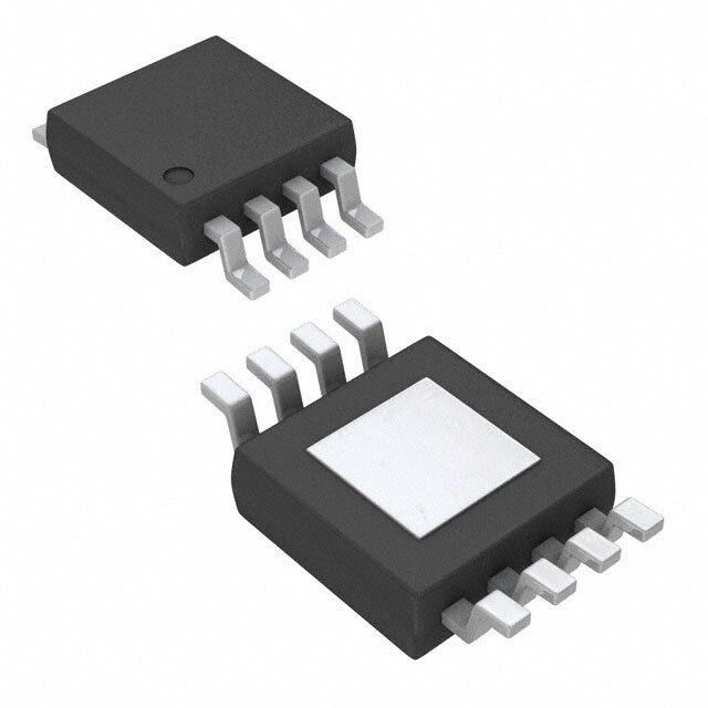
| 产品图片 |
|
| rohs | 符合RoHS无铅 / 符合限制有害物质指令(RoHS)规范要求 |
| 产品系列 | 电源管理 IC,稳压器—开关式稳压器,Texas Instruments TPS54610PWPSWIFT™ |
| 数据手册 | |
| 产品型号 | TPS54610PWP |
| PWM类型 | 电压模式 |
| 产品培训模块 | http://www.digikey.cn/PTM/IndividualPTM.page?site=cn&lang=zhs&ptm=16804http://www.digikey.cn/PTM/IndividualPTM.page?site=cn&lang=zhs&ptm=25755 |
| 产品目录页面 | |
| 产品种类 | 稳压器—开关式稳压器 |
| 供应商器件封装 | 28-HTSSOP |
| 其它名称 | 296-12123-5 |
| 制造商产品页 | http://www.ti.com/general/docs/suppproductinfo.tsp?distId=10&orderablePartNumber=TPS54610PWP |
| 包装 | 管件 |
| 单位重量 | 118.500 mg |
| 同步整流器 | 是 |
| 商标 | Texas Instruments |
| 安装类型 | 表面贴装 |
| 安装风格 | SMD/SMT |
| 宽度 | 4.4 mm |
| 封装 | Tube |
| 封装/外壳 | 28-SOIC(0.173",4.40mm 宽)裸露焊盘 |
| 封装/箱体 | HTSSOP-28 |
| 工作温度 | -40°C ~ 85°C |
| 工作温度范围 | - 40 C to + 85 C |
| 工厂包装数量 | 50 |
| 开关频率 | 700 kHz |
| 拓扑结构 | Buck |
| 最大工作温度 | + 85 C |
| 最大输入电压 | 6 V |
| 最小工作温度 | - 40 C |
| 最小输入电压 | 3 V |
| 标准包装 | 50 |
| 电压-输入 | 3 V ~ 6 V |
| 电压-输出 | 0.9 V ~ 4.5 V |
| 电流-输出 | 6A |
| 类型 | 降压(降压) |
| 系列 | TPS54610 |
| 设计资源 | http://www.digikey.com/product-highlights/cn/zh/texas-instruments-webench-design-center/3176 |
| 负载调节 | 0.03 % / A |
| 输入电压 | 3 V to 6 V |
| 输出数 | 1 |
| 输出电压 | 0.9 V to 3.3 V |
| 输出电流 | 6 A |
| 输出端数量 | 1 Output |
| 输出类型 | 可调式 |
| 配用 | /product-detail/zh/TPS54610EVM-192/296-13576-ND/486535/product-detail/zh/TPS54610EVM-213/296-20596-ND/562066/product-detail/zh/TPS54680EVM/296-20599-ND/562086/product-detail/zh/XILINXPWR-082/296-17304-ND/684804 |
| 频率-开关 | 350kHz,550kHz |


- 商务部:美国ITC正式对集成电路等产品启动337调查
- 曝三星4nm工艺存在良率问题 高通将骁龙8 Gen1或转产台积电
- 太阳诱电将投资9.5亿元在常州建新厂生产MLCC 预计2023年完工
- 英特尔发布欧洲新工厂建设计划 深化IDM 2.0 战略
- 台积电先进制程称霸业界 有大客户加持明年业绩稳了
- 达到5530亿美元!SIA预计今年全球半导体销售额将创下新高
- 英特尔拟将自动驾驶子公司Mobileye上市 估值或超500亿美元
- 三星加码芯片和SET,合并消费电子和移动部门,撤换高东真等 CEO
- 三星电子宣布重大人事变动 还合并消费电子和移动部门
- 海关总署:前11个月进口集成电路产品价值2.52万亿元 增长14.8%


PDF Datasheet 数据手册内容提取
Product Order Technical Tools & Support & Reference Folder Now Documents Software Community Design TPS54610 SLVS398H–JUNE2001–REVISEDOCTOBER2015 TPS54610 3-V to 6-V Input, 6-A Output Synchronous Buck PWM Switcher with Integrated FETs 1 Features 3 Description • 30-mΩ,12-APeakMOSFETSwitchesforHigh The TPS54610 low-input voltage high-output current 1 synchronous buck PWM converter integrates all Efficiencyat6-AContinuousOutputSourceor required active components. Included on the SinkCurrent substrate with the listed features are a true, high • AdjustableOutputVoltageDownto0.9VWith performance, voltage error amplifier that enables 1.0%Accuracy maximum performance and flexibility in choosing the • WidePWMFrequency:Fixed350kHz,550kHz output filter L and C components; an undervoltage- orAdjustable280kHzto700kHz lockout circuit to prevent start-up until the input voltage reaches 3 V; an internally or externally set • Synchronizableto700kHz slow-start circuit to limit inrush currents; and a power • LoadProtectedbyPeakCurrentLimitand good output useful for processor/logic reset, fault ThermalShutdown signaling,andsupplysequencing. • IntegratedSolutionReducesBoardAreaand The TPS54610 is available in a thermally enhanced ComponentCount 28-pin HTSSOP (PWP) PowerPAD™ package, which • SWIFTDocumentation,ApplicationNotes,and eliminates bulky heatsinks. TI provides evaluation DesignSoftware:www.ti.com/swift modules to aid in quickly achieving high-performance power supply designs to meet aggressive equipment 2 Applications developmentcycles. • Low-Voltage,High-DensityDistributedPower DeviceInformation(1) Systems DEVICENAME PACKAGE BODYSIZE(NOM) • PointofLoadRegulationforHigh TPS54610 HTSSOP(28) 9.70mmx6.40mm PerformanceDSPs,FPGAs,ASICsand Microprocessors • Broadband,NetworkingandOptical CommunicationsInfrastructure (1) Forallavailablepackages,seetheorderableaddendumat • PortableComputing/NotebookPCs theendofthedatasheet. SimplifiedSchematic Efficiencyat350kHz Input Output 100 VIN PH 95 TPS54610 BOOT 90 PGND 85 % VBIAS VSENSE − 80 AGND COMP ncy 75 e Effici 70 65 60 VI= 5 V, VO= 3.3 V 55 50 0 1 2 3 4 5 6 Load Current−A 1 An IMPORTANT NOTICE at the end of this data sheet addresses availability, warranty, changes, use in safety-critical applications, intellectualpropertymattersandotherimportantdisclaimers.PRODUCTIONDATA.
TPS54610 SLVS398H–JUNE2001–REVISEDOCTOBER2015 www.ti.com Table of Contents 1 Features.................................................................. 1 8.4 DeviceFunctionalModes........................................13 2 Applications........................................................... 1 9 ApplicationandImplementation........................ 14 3 Description............................................................. 1 9.1 ApplicationInformation............................................14 4 RevisionHistory..................................................... 2 9.2 TypicalApplications................................................14 5 DeviceComparisonTable..................................... 3 10 PowerSupplyRecommendations..................... 19 6 PinConfigurationandFunctions......................... 3 11 Layout................................................................... 19 11.1 LayoutGuidelines.................................................19 7 Specifications......................................................... 4 11.2 LayoutExample....................................................20 7.1 AbsoluteMaximumRatings......................................4 11.3 ThermalConsiderations........................................21 7.2 ESDRatings..............................................................4 12 DeviceandDocumentationSupport................. 22 7.3 RecommendedOperatingConditions.......................4 7.4 ThermalInformation..................................................5 12.1 DeviceSupport......................................................22 7.5 ElectricalCharacteristics...........................................5 12.2 ReceivingNotificationofDocumentationUpdates22 7.6 DissipationRatings...................................................7 12.3 CommunityResources..........................................22 7.7 TypicalCharacteristics..............................................8 12.4 Trademarks...........................................................22 12.5 ElectrostaticDischargeCaution............................22 8 DetailedDescription............................................ 10 12.6 Glossary................................................................22 8.1 Overview.................................................................10 13 Mechanical,Packaging,andOrderable 8.2 FunctionalBlockDiagram.......................................10 Information........................................................... 22 8.3 FeatureDescription.................................................11 4 Revision History NOTE:Pagenumbersforpreviousrevisionsmaydifferfrompagenumbersinthecurrentversion. ChangesfromRevisionG(October2015)toRevisionH Page • Editorialchangesonly;notechnicalchanges ....................................................................................................................... 1 ChangesfromRevisionF(April2007)toRevisionG Page • AddedPinConfigurationandFunctionssection,ESDRatingstable,FeatureDescriptionsection,DeviceFunctional Modes,ApplicationandImplementationsection,PowerSupplyRecommendationssection,Layoutsection,Device andDocumentationSupportsection,andMechanical,Packaging,andOrderableInformationsection .............................. 1 2 SubmitDocumentationFeedback Copyright©2001–2015,TexasInstrumentsIncorporated ProductFolderLinks:TPS54610
TPS54610 www.ti.com SLVS398H–JUNE2001–REVISEDOCTOBER2015 5 Device Comparison Table DEVICE OUTPUTVOLTAGE DEVICE OUTPUTVOLTAGE DEVICE OUTPUTVOLTAGE TPS54611 0.9V TPS54614 1.8V TPS54672 DDR Memory/Adjustable TPS54612 1.2V TPS54615 2.5V TPS54673 Pre-bias/Adjustable TPS54613 1.5V TPS54616 3.3V TPS54680 Sequencing/Adjustable 6 Pin Configuration and Functions PWPPackage 28-PinHTSSOPWithExposedThermalPad TopView AGND 1 28 RT VSENSE 2 27 SYNC COMP 3 26 SS/ENA PWRGD 4 25 VBIAS BOOT 5 24 VIN PH 6 23 VIN PH 7 THERMAL 22 VIN PH 8 PAD 21 VIN PH 9 20 VIN PH 10 19 PGND PH 11 18 PGND PH 12 17 PGND PH 13 16 PGND PH 14 15 PGND PinFunctions PIN TYPE(1) DESCRIPTION NAME NO. Analogground.Returnforcompensationnetwork/outputdivider,slow-startcapacitor,VBIAS AGND 1 G capacitor,RTresistorandSYNCpin.ConnectPowerPAD™toAGND. Bootstrapoutput.0.022-μFto0.1-μFlow-ESRcapacitorconnectedfromBOOTtoPH BOOT 5 S generatesfloatingdriveforthehigh-sideFETdriver. COMP 3 Erroramplifieroutput.ConnectfrequencycompensationnetworkfromCOMPtoVSENSE Powerground.Highcurrentreturnforthelow-sidedriverandpowerMOSFET.Connect PGND 15-19 G PGNDwithlargecopperareastotheinputandoutputsupplyreturns,andnegativepinsof theinputandoutputcapacitors.AsinglepointconnectiontoAGNDisrecommended. Phaseoutput.Junctionoftheinternalhigh-sideandlow-sidepowerMOSFETs,andoutput PH 6-14 O inductor. Powergoodopendrainoutput.HighwhenVSENSE≥90%V ,otherwisePWRGDislow. PWRGD 4 O ref NotethatoutputislowwhenSS/ENAislowortheinternalshutdownsignalisactive. Frequencysettingresistorinput.ConnectaresistorfromRTtoAGNDtosettheswitching RT 28 I frequency.WhenusingtheSYNCpin,settheRTvalueforafrequencyatorslightlylower thantheexternaloscillatorfrequency. Slow-start/enableinput/output.Dualfunctionpinwhichprovideslogicinputtoenable/disable SS/ENA 26 I/O deviceoperationandcapacitorinputtoexternallysetthestart-uptime. Synchronizationinput.Dualfunctionpinwhichprovideslogicinputtosynchronizetoan SYNC 27 I/O externaloscillatororpinselectbetweentwointernallysetswitchingfrequencies.Whenused tosynchronizetoanexternalsignal,aresistormustbeconnectedtotheRTpin. Internalbiasregulatoroutput.Suppliesregulatedvoltagetointernalcircuitry.BypassVBIAS VBIAS 25 S pintoAGNDpinwithahighquality,low-ESR0.1-μFto1.0-μFceramiccapacitor. (1) I=Input,O=Output,S=Supply,G=GroundReturn Copyright©2001–2015,TexasInstrumentsIncorporated SubmitDocumentationFeedback 3 ProductFolderLinks:TPS54610
TPS54610 SLVS398H–JUNE2001–REVISEDOCTOBER2015 www.ti.com PinFunctions(continued) PIN TYPE(1) DESCRIPTION NAME NO. InputsupplyforthepowerMOSFETswitchesandinternalbiasregulator.BypassVINpinsto VIN 20-24 I PGNDpinsclosetodevicepackagewithahighquality,low-ESR10-μFceramiccapacitor. Erroramplifierinvertinginput.Connecttooutputvoltagethroughcompensation VSENSE 2 I network/outputdivider. 7 Specifications 7.1 Absolute Maximum Ratings overoperatingfree-airtemperaturerangeunlessotherwisenoted(1) MIN MAX UNIT VIN,SS/ENA,SYNC –0.3 7 V RT –0.3 6 V V Inputvoltage I VSENSE –0.3 4 V BOOT –0.3 17 V VBIAS,COMP,PWRGD –0.3 7 V V Outputvoltage PH –0.6 10 V O PH(transient<10ns) –2 V PH InternallyLimited I Sourcecurrent O COMP,VBIAS 6 mA PH 12 A I Sinkcurrent COMP 6 mA S SS/ENA,PWRGD 10 mA Voltagedifferential AGNDtoPGND –0.3 0.3 V T Operatingvirtualjunctiontemperature –40 125 °C J T Storagetemperature –65 150 °C stg (1) StressesbeyondthoselistedunderAbsoluteMaximumRatingsmaycausepermanentdamagetothedevice.Thesearestressratings only,andfunctionaloperationofthedeviceattheseoranyotherconditionsbeyondthoseindicatedunderRecommendedOperating Conditionsisnotimplied.Exposuretoabsolute-maximum-ratedconditionsforextendedperiodsmayaffectdevicereliability. 7.2 ESD Ratings VALUE UNIT Humanbodymodel(HBM)perANSI/ESDA/JEDECJS- 001,allpins (1) –2000 V V Electrostaticdischarge (ESD) Chargeddevicemodel(CDM),perJEDECspecification JESD22-C101,allpins (2) –1500 V (1) JEDECdocumentJEP155statesthat500-VHBMallowssafemanufacturingwithastandardESDcontrolprocess. (2) JEDECdocumentJEP157statesthat250-VCDMallowssafemanufacturingwithastandardESDcontrolprocess. 7.3 Recommended Operating Conditions MIN NOM MAX UNIT Inputvoltage,V 3 6 V I Operatingjunctiontemperature,T –40 125 °C J 4 SubmitDocumentationFeedback Copyright©2001–2015,TexasInstrumentsIncorporated ProductFolderLinks:TPS54610
TPS54610 www.ti.com SLVS398H–JUNE2001–REVISEDOCTOBER2015 7.4 Thermal Information TPS54610 THERMALMETRIC(1) PWP(HTSSOP) UNIT 28PINS R Junction-to-ambientthermalresistance 31.0 °C/W θJA R Junction-to-case(top)thermalresistance 28.3 °C/W θJC(top) R Junction-to-boardthermalresistance 15.1 °C/W θJB ψ Junction-to-topcharacterizationparameter 0.7 °C/W JT ψ Junction-to-boardcharacterizationparameter 7.0 °C/W JB (1) Formoreinformationabouttraditionalandnewthermalmetrics,seetheSemiconductorandICPackageThermalMetricsapplication report,SPRA953. 7.5 Electrical Characteristics overoperatingfree-airtemperaturerangeunlessotherwisenoted PARAMETER TESTCONDITIONS MIN TYP MAX UNIT SUPPLYVOLTAGE,VIN Inputvoltagerange,VIN 3 6 V f =350kHz,SYNC≤0.8V,RTopen, s 11 15.8 PHpinopen I Quiescentcurrent f =550kHz,SYNC≥2.5V,RTopen, mA (Q) s 16 23.5 PHpinopen Shutdown,SS/ENA=0V 1 1.4 UNDERVOLTAGELOCKOUT Startthresholdvoltage,UVLO 2.95 3.0 V Stopthresholdvoltage,UVLO 2.70 2.80 V Hysteresisvoltage,UVLO 0.14 0.16 V Risingandfallingedgedeglitch,UVLO(1) 2.5 μs BIASVOLTAGE Outputvoltage,VBIAS I =0 2.70 2.80 2.90 V (VBIAS) Outputcurrent,VBIAS (2) 100 μA CUMULATIVEREFERENCE V Accuracy 0.882 0.891 0.900 V ref REGULATION I =3A,f =350kHz,T =85°C 0.04 Lineregulation(2) (3) L s J %/V I =3A,f =550kHz,T =85°C 0.04 L s J I =0Ato6A,f =350kHz,T =85°C 0.03 Loadregulation(1) (3) L s J %/A I =0Ato6A,f =550kHz,T =85°C 0.03 L s J OSCILLATOR SYNC≤0.8V,RTopen 280 350 420 Internallyset—freerunningfrequency kHz SYNC≥2.5V,RTopen 440 550 660 RT=180kΩ(1%resistortoAGND)(1) 252 280 308 Externallyset—freerunningfrequencyrange RT=100kΩ(1%resistortoAGND) 460 500 540 kHz RT=68kΩ(1%resistortoAGND)(1) 663 700 762 Highlevelthreshold,SYNC 2.5 V Lowlevelthreshold,SYNC 0.8 V Pulseduration,externalsynchronization, SYNC(1) 50 ns Frequencyrange,SYNC(1) 330 700 kHz (1) Specifiedbydesign (2) Staticresistiveloadsonly (3) SpecifiedbythecircuitusedinFigure10 Copyright©2001–2015,TexasInstrumentsIncorporated SubmitDocumentationFeedback 5 ProductFolderLinks:TPS54610
TPS54610 SLVS398H–JUNE2001–REVISEDOCTOBER2015 www.ti.com Electrical Characteristics (continued) overoperatingfree-airtemperaturerangeunlessotherwisenoted PARAMETER TESTCONDITIONS MIN TYP MAX UNIT Rampvalley(1) 0.75 V Rampamplitude(peak-to-peak)(1) 1 V Minimumcontrollableontime(1) 200 ns Maximumdutycycle 90% ERRORAMPLIFIER Erroramplifieropenloopvoltagegain 1kΩCOMPtoAGND(1) 90 110 dB Erroramplifierunitygainbandwidth Parallel10kΩ,160pFCOMPtoAGND(1) 3 5 MHz Erroramplifiercommonmodeinputvoltage PoweredbyinternalLDO(1) 0 VBIAS V range Inputbiascurrent,VSENSE VSENSE=V 60 250 nA ref Outputvoltageslewrate(symmetric),COMP 1 1.4 V/μs PWMCOMPARATOR PWMcomparatorpropagationdelay time,PWMcomparatorinputtoPHpin 10-mVoverdrive(1) 70 85 ns (excludingdeadtime) SLOW-START/ENABLE Enablethresholdvoltage,SS/ENA 0.82 1.20 1.40 V Enablehysteresisvoltage,SS/ENA 0.03 V Fallingedgedeglitch,SS/ENA(1) 2.5 μs Internalslow-starttime 2.6 3.35 4.1 ms Chargecurrent,SS/ENA SS/ENA=0V 3 5 8 μA Dischargecurrent,SS/ENA SS/ENA=1.2V,V =2.7V 2 2.3 4 mA I POWERGOOD Powergoodthresholdvoltage VSENSEfalling 90 %V ref Powergoodhysteresisvoltage(1) 3 %V ref Powergoodfallingedgedeglitch(1) 35 μs Outputsaturationvoltage,PWRGD I =2.5mA 0.18 0.3 V (sink) Leakagecurrent,PWRGD V=5.5V 1 μA I CURRENTLIMIT V =3VOutputshorted(1) 7.2 10 I Currentlimittrippoint A V=6VOutputshorted(1) 10 12 I Currentlimitleadingedgeblankingtime(1) 100 ns Currentlimittotalresponsetime(1) 200 ns THERMALSHUTDOWN Thermalshutdowntrippoint(1) 135 150 165 °C Thermalshutdownhysteresis(1) 10 °C OUTPUTPOWERMOSFETS V =6V(4) 26 47 I r PowerMOSFETswitches mΩ DS(on) V =3V(4) 36 65 I (4) MatchedMOSFETslow-sider productiontested,high-sider specifiedbydesign DS(on) DS(on) 6 SubmitDocumentationFeedback Copyright©2001–2015,TexasInstrumentsIncorporated ProductFolderLinks:TPS54610
TPS54610 www.ti.com SLVS398H–JUNE2001–REVISEDOCTOBER2015 7.6 Dissipation Ratings(1)(2) THERMALIMPEDANCE T =25°C T =70°C T =85°C PACKAGE A A A JUNCTION-TO-AMBIENT POWERRATING POWERRATING POWERRATING 28PinPWPwithsolder 18.2°C/W 5.49(3)W 3.02W 2.20W 28PinPWPwithout 40.5°C/W 2.48W 1.36W 0.99W solder (1) Testboardconditions: (a)3inch×3inch,4layers,thickness:0.062in (b)1.5oz.coppertraceslocatedonthetopofthePCB (c)1.5oz.copperplanelocatedonthebottomofthePCB (d)0.5oz.copperplanesonthe2innerlayers (e)12thermalvias.SeeFigure23 (2) ThermalmetricsshowninThermalInformationrefertoJEDECHighKboard.Metricsinthistablerefertothetestboardconditionslisted below. (3) Maximumpowerdissipationmaybelimitedbyovercurrentprotection Copyright©2001–2015,TexasInstrumentsIncorporated SubmitDocumentationFeedback 7 ProductFolderLinks:TPS54610
TPS54610 SLVS398H–JUNE2001–REVISEDOCTOBER2015 www.ti.com 7.7 Typical Characteristics 60 60 W W m IO=6A m − 50 − 50 nce nce IO=6A a a stst 40 stst 40 e e R R e e Stat 30 Stat 30 n- n- O O ce 20 ce 20 ur ur o o S S n n ai 10 ai 10 Dr Dr 0 0 −40 0 25 85 125 −40 0 25 85 125 TJ−Junction Temperature−°C TJ−Junction Temperature−°C VIN=3.3V VIN=5V Figure1.Drain-SourceOn-StateResistancevs Figure2.Drain-SourceOn-StateResistancevs JunctionTemperature JunctionTemperature 750 800 kHz kHz Oscillator Frequency− 456555000 SYNC≥2.5V Oscillator Frequency− 567000000 RRTT==16080kk −Internally Set 350 SYNC≤0.8V Externally Set 340000 RT=180k f 250 f− 200 −40 0 25 85 125 −40 0 25 85 125 TJ−Junction Temperature−°C TJ−Junction Temperature−°C Figure3.InternallySetOscillatorFrequencyvs Figure4.ExternallySetOscillatorFrequencyvs JunctionTemperature JunctionTemperature 0.895 5 4.5 0.893 4 V W − − 3.5 ge Reference 00..888991 owerLosses 2.523 VI=3.3V a P −Voltef0.887 Device 1.51 VI=5V Vr 0.5 0.885 0 −40 0 25 85 125 0 1 2 3 4 5 6 7 8 TJ−Junction Temperature−°C IL−Load Current−A T =125°C f =700kHz J s Figure5.VoltageReferencevsJunctionTemperature Figure6.DevicePowerLossesatT =125°Cvs J LoadCurrent 8 SubmitDocumentationFeedback Copyright©2001–2015,TexasInstrumentsIncorporated ProductFolderLinks:TPS54610
TPS54610 www.ti.com SLVS398H–JUNE2001–REVISEDOCTOBER2015 Typical Characteristics (continued) 0.895 140 0 120 −20 V − 0.893 −40 n 100 oltut Vage Regulatio 00..888991 fs=550kHz Gain−dB 468000 GaPihnase −−−−1186200000Phase−Degrees p −140 Out 20 − 0.887 −160 O V 0 −180 0.885 −20 −200 3 3.5 4 4.5 5 5.5 6 1 10 100 1k 10k 100k 1M 10M VI−Input Voltage−V f−Frequency−Hz TJ=85°C IO=3A RL=10kΩ CL=160pF TA=25°C Figure7.OutputVoltageRegulationvsInputVoltage Figure8.ErrorAmplifierOpenLoopResponse 3.80 3.65 s m − 3.50 e m art Ti 3.35 St w- 3.20 o Sl nal 3.05 er nt I 2.90 2.75 −40 0 25 85 125 TJ−Junction Temperature−°C Figure9.InternalSlow-StartTimevsJunctionTemperature Copyright©2001–2015,TexasInstrumentsIncorporated SubmitDocumentationFeedback 9 ProductFolderLinks:TPS54610
TPS54610 SLVS398H–JUNE2001–REVISEDOCTOBER2015 www.ti.com 8 Detailed Description 8.1 Overview The TPS54610 low-input voltage high-output current synchronous buck PWM converter integrates all required active components. Included on the substrate with the listed features are a true, high performance, voltage error amplifier that enables maximum performance and flexibility in choosing the output filter L and C components; an under-voltage-lockout circuit to prevent start-up until the input voltage reaches 3 V; an internally or externally set slow-start circuit to limit inrush currents; and a power good output useful for processor/logic reset, fault signaling, andsupplysequencing. 8.2 Functional Block Diagram AGND VBIAS VIN Enable Comparator SS/ENA VBIAS REG Falling SHUTDOWN 1.2V Edge ILIM VIN Deglitch Thermal Comparator 3−6V Hysteresis:0.03V 2.5µs Shutdown Leading 150°C Edge VINUVLO Blanking Comparator Falling 100ns and VIN Rising BOOT 2.95V Edge Hysteresis:0.16V Deglitch 30mW 2.5µs SS_DIS SHUTDOWN PH LOUT VO Internal/External Slow-start + (InternalSlow-startTime=3.35ms − R Q AdaptiveDead-Time CO and Error S ControlLogic Amplifier PWM Reference Comparator VIN VREF=0.891V 30mW OSC PGND Powergood Comparator PWRGD VSENSE Falling 0.90Vref Edge TPS54610 Deglitch Hysteresis:0.03Vref SHUTDOWN 35µs VSENSE COMP RT SYNC 10 SubmitDocumentationFeedback Copyright©2001–2015,TexasInstrumentsIncorporated ProductFolderLinks:TPS54610
TPS54610 www.ti.com SLVS398H–JUNE2001–REVISEDOCTOBER2015 8.3 Feature Description 8.3.1 UndervoltageLockout(UVLO) The TPS54610 incorporates an UVLO to keep the device disabled when the input voltage (VIN) is insufficient. During power up, internal circuits are held inactive until VIN exceeds the nominal UVLO threshold voltage of 2.95 V. Once the UVLO start threshold is reached, device start-up begins. The device operates until VIN falls below the nominal UVLO stop threshold of 2.8 V. Hysteresis in the UVLO comparator, and a 2.5-μs rising and falling edgedeglitchcircuitreducethelikelihoodofshuttingthedevicedownduetonoiseonVIN. 8.3.2 SlowStart/Enable(SS/ENA) The slow-start/enable pin provides two functions. First, the pin acts as an enable (shutdown) control by keeping the device turned off until the voltage exceeds the start threshold voltage of approximately 1.2 V. When SS/ENA exceeds the enable threshold, device start-up begins. The reference voltage fed to the error amplifier is linearly ramped up from 0 V to 0.891 V in 3.35 ms. Similarly, the converter output voltage reaches regulation in approximately 3.35 ms. Voltage hysteresis and a 2.5-μs falling edge deglitch circuit reduce the likelihood of triggeringtheenableduetonoise. The second function of the SS/ENA pin provides an external means of extending the slow-start time with a low- valuecapacitorconnectedbetweenSS/ENAandAGND. Adding a capacitor to the SS/ENA pin has two effects on start-up. First, a delay occurs between release of the SS/ENA pin and start-up of the output. The delay is proportional to the slow-start capacitor value and lasts until theSS/ENApinreachestheenablethreshold.Thestart-updelayisapproximately: 1.2V t =C ´ d (SS) 5mA (1) Second,astheoutputbecomesactive,abrieframp-upat the internal slow-start rate may be observed before the externally set slow-start rate takes control and the output rises at a rate proportional to the slow-start capacitor. Theslow-starttimesetbythecapacitorisapproximately: 0.7V t =C ´ (SS) (SS) 5mA (2) The actual slow-start time is likely to be less than the above approximation due to the brief ramp-up at the internalrate. 8.3.3 VBIASRegulator(VBIAS) The VBIAS regulator provides internal analog and digital blocks with a stable supply voltage over variations in junction temperature and input voltage. A high quality, low-ESR, ceramic bypass capacitor is required on the VBIAS pin. X7R or X5R grade dielectrics are recommended because their values are more stable over temperature.ThebypasscapacitormustbeplacedclosetotheVBIASpinandreturnedtoAGND. External loading on VBIAS is allowed, with the caution that internal circuits require a minimum VBIAS of 2.70V, andexternalloadsonVBIASwithacordigitalswitchingnoisemaydegradeperformance.TheVBIAS pin may be usefulasareferencevoltageforexternalcircuits. 8.3.4 VoltageReference The voltage reference system produces a precise V signal by scaling the output of a temperature stable ref bandgap circuit. During manufacture, the bandgap and scaling circuits are trimmed to produce 0.891 V at the output of the error amplifier, with the amplifier connected as a voltage follower. The trim procedure adds to the highprecisionregulationoftheTPS54610,sinceitcancelsoffseterrorsinthescaleanderroramplifiercircuits. 8.3.5 OscillatorandPWMRamp The oscillator frequency can be set to internally fixed values of 350 kHz or 550 kHz using the SYNC pin as a static digital input. If a different frequency of operation is required for the application, the oscillator frequency can be externally adjusted from 280 to 700 kHz by connecting a resistor between the RT pin and AGND and floating the SYNC pin. The switching frequency is approximated by the following equation, where R is the resistance fromRTtoAGND: Copyright©2001–2015,TexasInstrumentsIncorporated SubmitDocumentationFeedback 11 ProductFolderLinks:TPS54610
TPS54610 SLVS398H–JUNE2001–REVISEDOCTOBER2015 www.ti.com Feature Description (continued) 100kW SwitchingFrequency= ´500[kHz] R (3) ExternalsynchronizationofthePWMrampispossibleoverthefrequencyrangeof330kHzto700kHzby driving a synchronization signal into SYNC and connecting a resistor from RT to AGND. Choose a resistor between the RT and AGND which sets the free running frequency to 80% of the synchronization signal. Table 1 summarizes thefrequencyselectionconfigurations: Table1.SwitchingFrequency/SynchronizationConfiguration SWITCHINGFREQUENCY SYNCPIN RTPIN 350kHz,internallyset FloatorAGND Float 550kHz,internallyset ≥2.5V Float Externallyset280kHzto700kHz Float R=180kΩto68kΩ R=RTvaluefor80%ofexternal Externallysynchronizedfrequency Synchronizationsignal synchronizationfrequency 8.3.6 ErrorAmplifier The high performance, wide bandwidth, voltage error amplifier sets the TPS54610 apart from most dc/dc converters. The user is given the flexibility to use a wide range of output L and C filter components to suit the particular application needs. Type 2 or type 3 compensation can be employed using external compensation components. 8.3.7 PWMControl Signalsfromtheerroramplifieroutput,oscillator,andcurrentlimitcircuitareprocessedbythePWMcontrol logic. Referring to the internal block diagram, the control logic includes the PWM comparator, OR gate, PWM latch, and portions of the adaptive dead-time and control logic block. During steady-state operation below the current limit threshold, the PWM comparator output and oscillator pulse train alternately reset and set the PWM latch. Once the PWM latch is reset, the low-side FET remains on for a minimum duration set by the oscillator pulse width. During this period, the PWM ramp discharges rapidly to its valley voltage. When the ramp begins to charge back up, the low-side FET turns off and high-side FET turns on. As the PWM ramp voltage exceeds the error amplifier output voltage, the PWM comparator resets the latch, thus turning off the high-side FET and turning on the low-side FET. The low-side FET remains on until the next oscillator pulse discharges the PWM ramp. During transient conditions, the error amplifier output could be below the PWM ramp valley voltage or above the PWM peak voltage. If the error amplifier is high, the PWM latch is never reset, and the high-side FET remains on until the oscillator pulse signals the control logic to turn the high-side FET off and the low-side FET on. The device operates at its maximum duty cycle until the output voltage rises to the regulation set-point, setting VSENSE to approximately the same voltage as VREF. If the error amplifier output is low, the PWM latch is continually reset and the high-side FET does not turn on. The low-side FET remains on until the VSENSE voltage decreases to a range that allows the PWM comparator to change states. The TPS54610 is capable of sinkingcurrentcontinuouslyuntiltheoutputreachestheregulationset-point. If the current limit comparator trips for longer than 100 ns, the PWM latch resets before the PWM ramp exceeds the error amplifier output. The high-side FET turns off and low-side FET turns on to decrease the energy in the output inductor and consequently the output current. This process is repeated each cycle in which the current limitcomparatoristripped. 8.3.8 Dead-TimeControlandMOSFETDrivers Adaptive dead-time control prevents shoot-through current from flowing in both N-channel power MOSFETs during the switching transitions by actively controlling the turnon times of the MOSFET drivers. The high-side driver does not turn on until the voltage at the gate of the low-side FET is below 2 V. While the low-side driver doesnotturnonuntilthevoltageatthegateofthehigh-sideMOSFETisbelow2V. 12 SubmitDocumentationFeedback Copyright©2001–2015,TexasInstrumentsIncorporated ProductFolderLinks:TPS54610
TPS54610 www.ti.com SLVS398H–JUNE2001–REVISEDOCTOBER2015 The high-side and low-side drivers are designed with 300-mA source and sink capability to quickly drive the power MOSFETs gates. The low-side driver is supplied from VIN, while the high-side drive is supplied from the BOOT pin. A bootstrap circuit uses an external BOOT capacitor and an internal 2.5-Ω bootstrap switch connected between the VIN and BOOT pins. The integrated bootstrap switch improves drive efficiency and reducesexternalcomponentcount. 8.3.9 OvercurrentProtection The cycle-by-cycle current limiting is achieved by sensing the current flowing through the high-side MOSFET and comparing this signal to a preset overcurrent threshold. The high side MOSFET is turned off within 200 ns of reaching the current limit threshold. A 100-ns leading edge blanking circuit prevents current limit false tripping. Current limit detection occurs only when current flows from VIN to PH when sourcing current to the output filter. Loadprotectionduringcurrentsinkoperationisprovidedbythermalshutdown. 8.3.10 ThermalShutdown The device uses the thermal shutdown to turn off the power MOSFETs and disable the controller if the junction temperature exceeds 150°C. The device is released from shutdown automatically when the junction temperature decreasesto10°Cbelowthethermalshutdowntrippoint,andstartsupundercontroloftheslow-startcircuit. Thermal shutdown provides protection when an overload condition is sustained for several milliseconds. With a persistent fault condition, the device cycles continuously; starting up by control of the soft-start circuit, heating up due to the fault condition, and then shutting down upon reaching the thermal shutdown trip point. This sequence repeatsuntilthefaultconditionisremoved. 8.3.11 Power-Good(PWRGD) The power good circuit monitors for under voltage conditions on VSENSE. If the voltage on VSENSE is 10% below the reference voltage, the open-drain PWRGD output is pulled low. PWRGD is also pulled low if VIN is less than the UVLO threshold or SS/ENA is low, or a thermal shutdown occurs. When VIN ≥ UVLO threshold, SS/ENA ≥ enable threshold, and VSENSE > 90% of V , the open drain output of the PWRGD pin is high. A ref hysteresis voltage equal to 3% of V and a 35-μs falling edge deglitch circuit prevent tripping of the power good ref comparatorduetohighfrequencynoise. 8.4 Device Functional Modes 8.4.1 ContinuousConductionMode The TPS54610 devices operate in continuous conduction mode, that is, the low-side MOSFET runs fully complimentarytothehigh-sideMOSFETregardlessofoutputcurrent. 8.4.2 SwitchingFrequencySelection/Synchronization Depending on the configuration of the RT and SYNC pins, the TPS54610 can be configured to switch at 350 kHz, or 550 kHz without external components, or any frequency between 280 kHz and 700 kHz as configured by a resistor from the RT pin to ground. The TPS54610 can also be synchronized to an external clock using the SYNCpin.SeeTable1formoreinformation. Copyright©2001–2015,TexasInstrumentsIncorporated SubmitDocumentationFeedback 13 ProductFolderLinks:TPS54610
TPS54610 SLVS398H–JUNE2001–REVISEDOCTOBER2015 www.ti.com 9 Application and Implementation NOTE Information in the following applications sections is not part of the TI component specification, and TI does not warrant its accuracy or completeness. TI’s customers are responsible for determining suitability of components for their purposes. Customers should validateandtesttheirdesignimplementationtoconfirmsystemfunctionality. 9.1 Application Information The TPS54610 is a 3 V to 6 V input, 6 A output synchronous buck PWM switcher. Ideal applications are: broadband,networkingandopticalcommunicationsinfrastructure,andportablecomputing/notebookPCs. 9.2 Typical Applications 9.2.1 HighFrequencySwitchingRegulatorUsingCeramicOutputCapacitors Figure 10 shows the schematic diagram for a typical TPS54610 application. The TPS54610 (U1) can provide greaterthan6Aofoutputcurrentatanominaloutputvoltageof3.3V. VI + C2 U1 220µF TPS54610PWP C8 10 V 10µF 28 24 RT VIN R2 23 10 kW VIN 27 22 SYNC VIN 21 VIN L1 26 SS/ENA VIN 20 4.7µH 14 PH VO 25 VBIAS PH 13 + C9 + C10 C11 C1 12 470µF 470mF 100 pF 0.047µF PH 4 V 4 V PWRGD 4 11 PWRGD PH 10 C4 PH 3 9 0.1µF COMP PH 8 PH 7 PH 6 PH C7 2 5 VSENSE BOOT 19 PGND 0.047µF 18 PGND 17 PGND 1 16 AGND PGND C5 15 C3 5600 pF PGND 120 pF POWERPAD R1 9.09 kW C6 R5 1.74 kW 8200 pF R3 3.74 kW R4 10 kW Figure10. ApplicationCircuit 14 SubmitDocumentationFeedback Copyright©2001–2015,TexasInstrumentsIncorporated ProductFolderLinks:TPS54610
TPS54610 www.ti.com SLVS398H–JUNE2001–REVISEDOCTOBER2015 Typical Applications (continued) 9.2.1.1 DesignRequirements This guide illustrates the design of a high frequency switching regulator using ceramic output capacitors. A few parameters must be known in order to start the design process. These requirements are typically determined at thesystemlevel.Forthisexample,startwiththefollowingknownparameters: Table2.DesignParameters DESIGNPARAMETER EXAMPLEVALUE OutputVoltage 3.3V MaximumOutputCurrent 6A InputVoltage 6V 9.2.1.2 DetailedDesignProcedure 9.2.1.2.1 ComponentSelection The values for the components used in this design example were selected using the SWIFT designer software tool. SWIFT designer provides a complete design environment for developing dc-dc converters using the TPS54610. 9.2.1.2.2 InputFilter The input to the circuit is a nominal 5 VDC. The input filter C2 is a 220-μF POSCAP capacitor, with a maximum allowable ripple current of 3 A. C8 provides high frequency decoupling of the TPS54610 from the input supply and must be located as close as possible to the device. Ripple current is carried in both C2 and C8, and the returnpathtoPGNDmustavoidthecurrentcirculatingintheoutputcapacitorsC9andC10. 9.2.1.2.3 FeedbackCircuit The resistor divider network of R3 and R4 sets the output voltage for the circuit at 3.3 V. R4, along with R1, R5, C3,C5,andC6formtheloopcompensationnetworkforthecircuit.Forthisdesign,aType3topologyisused. 9.2.1.2.4 OperatingFrequency In the application circuit, the 350 kHz operation is selected by leaving RT and SYNC open. Connecting a 180kΩ to 68 kΩ resistor between RT (pin 28) and analog ground can be used to set the switching frequency to 280kHz to700kHz.TocalculatetheRTresistor,usetheequationbelow: 500kHz R= ´100[kW] SwitchingFrequency (4) 9.2.1.2.5 OutputFilter Theoutputfilteris composed of a 4.7-μH inductor and two 470-μF capacitors. The inductor is a low dc resistance (12 mΩ) type, Coiltronics UP3B-4R7. The capacitors used are 4-V POSCAP types with a maximum ESR of 0.040Ω.Thefeedbackloopiscompensatedsothattheunitygainfrequencyisapproximately25kHz. Copyright©2001–2015,TexasInstrumentsIncorporated SubmitDocumentationFeedback 15 ProductFolderLinks:TPS54610
TPS54610 SLVS398H–JUNE2001–REVISEDOCTOBER2015 www.ti.com 9.2.1.3 ApplicationCurves 100 100 95 95 90 90 85 85 % 80 VO=2.5V % 80 VO=3.3V cy− 75 VO=1.8V cy− 75 VO=1.8V n n e e ci 70 ci 70 Effi VO=1.2V Effi VO=1.2V 65 65 60 60 55 55 50 50 0 1 2 3 4 5 6 7 0 1 2 3 4 5 6 7 IO−Output Current−A IO−Output Current−A V =3.3V f=550kHz L=4.7µH V =5V f=550kHz L=4.7µH I I T =25°C T =25°C A A Figure11.EfficiencyvsOutputCurrent Figure12.EfficiencyvsOutputCurrent 1.004 1.002 1.003 1.0015 IO=6A 1.002 1.001 Load Regulation01..9090911 Load Regulation01..909090155 NoLoad IO=3A 0.998 0.999 0.997 0.9985 0.996 0.998 0 1 2 3 4 5 6 4 4.5 5 5.5 6 IO−Output Current−A VI−Input Voltage−V VI=5V f=550kHz VO=3.3V VI=5V f=550kHz VO=3.3V TA=25°C TA=25°C Figure13.LoadRegulationvsOutputCurrent Figure14.LineRegulationvsInputVoltage 60 180 125 115 105 40 135 C ° 95 − Gain−dB 20 Gain Phase 90 Phase−Degrees bienemperat Tture 56785555 SAarefeaOperating VI=3.3V VI=5V 0 45 m A 45 35 −20 0 25 100 1k 10k 100k 1M 0 1 2 3 84 5 6 7 f−Frequency−Hz IO−Output Current−A VI=5V f=550kHz VO=3.3V TJ=125°C fs=700kHz T =25°C I =6A A O Figure15.LoopResponse Figure16.AmbientTemperaturevsLoadCurrent 16 SubmitDocumentationFeedback Copyright©2001–2015,TexasInstrumentsIncorporated ProductFolderLinks:TPS54610
TPS54610 www.ti.com SLVS398H–JUNE2001–REVISEDOCTOBER2015 v di V/ m mV/div e - 50 0 ag utput Ripple Voltage - 1 Output Volt Current- 2A/div O ut p ut O t-Time = 1ms/div t-Time = 100ms/div VI=5V VO=3.3V 6A,350kHz VI=5V 1Ato5A Figure17.OutputRippleVoltage Figure18.LoadTransientResponse v di V/ 2 e - g a olt V ut p n I v di V/ 2 - e g a olt V ut p ut O t-Time = 2 ms/div V =5V NoSlow-StartCap I Figure19.Slow-StartTiming Copyright©2001–2015,TexasInstrumentsIncorporated SubmitDocumentationFeedback 17 ProductFolderLinks:TPS54610
TPS54610 SLVS398H–JUNE2001–REVISEDOCTOBER2015 www.ti.com 9.2.2 HighFrequencyApplication Figure 20 shows the schematic diagram for a reduced size, high frequency application using the TPS54610. The TPS54610 (U1) can provide up to 6 A of output current at a nominal outputvoltage of 1.8 V. A small size 0.56 uH inductoris used and the switching frequency is set to 680 kHz by R1. The compensation network is optimized for fasttransientresponseasshowninFigure20. VI U1 C1 C2 TPS54610PWP 10µF 10µF R1 28 24 RT VIN 71.5 kW 23 VIN 27 22 SYNC VIN 21 VIN C3 26 20 SS/ENA VIN 0.047µF 14 PH C4 25 13 VBIAS PH 1µF 12 PH 4 11 PWRGD PH 10 C5 PH R2 3 9 COMP PH 10 kW 8 C6 470 pF PH L1 PH 7 0.56µH 6 470 pF PH VO 2 VSENSE BOOT 5 C7 + C8 + C9 C10 19 150µF 150µF 1 pF PGND 0.047µF R5 PGND 18 1.47 kW 17 R4 R3 1 PGND 16 2.4W 39W AGND PGND 15 PGND C11 R6 POWERPAD 3300 pF 1.5 kW C12 0.012µF Figure20. SmallSize,HighFrequencyDesign 9.2.2.1 DesignRequirements RefertoDesignRequirementsfortheHighFrequencyApplicationDesignRequirements. 9.2.2.2 DetailedDesignProcedure RefertoDetailedDesignProcedurefortheHighFrequencyApplicationDetailedDesignProcedure. 18 SubmitDocumentationFeedback Copyright©2001–2015,TexasInstrumentsIncorporated ProductFolderLinks:TPS54610
TPS54610 www.ti.com SLVS398H–JUNE2001–REVISEDOCTOBER2015 9.2.2.3 ApplicationCurve div div V/ A/ m 2 0 5 10µs/div Figure21. TransientResponse,1.5-Ato4.5-AStep 10 Power Supply Recommendations The device is designed to operate from an input voltage supply range between 3 V and 6 V. This input supply should be well regulated. If the input supply is located more than a few inches from the TPS54610 converter additionalbulkcapacitancemayberequired. 11 Layout 11.1 Layout Guidelines • For proper thermal performance, the exposed thermal PowerPAD underneath the integrated circuit package mustbesolderedtotheprinted-circuitboard. • For good thermal performance, the PowerPAD underneath the integrated circuit TPS54610 needs to be solderedwelltotheprinted-circuitboard. • The VIN pins are connected together on the printed-circuit board (PCB) and bypassed with a low-ESR ceramic-bypasscapacitor. • Care should be taken to minimize the loop area formed by the bypass capacitor connections, the VIN pins, andtheTPS54610groundpins. • The minimum recommended bypass capacitance is 10-mF ceramic capacitor with a X5R or X7R dielectric andtheoptimumplacementisclosesttotheVINpinsandthePGNDpins. • The TPS54610 has two internal grounds (analog and power). Inside the TPS54610, the analog ground ties to all of the noise sensitive signals, while the power ground ties to the noisier power signals. Noise injected between the two grounds can degrade the performance of the TPS54610, particularly at higher output currents. • However, ground noise on an analog ground plane can also cause problems with some of the control and biassignals.Therefore,separateanalogandpowergroundtracesarerecommended. • There is an area of ground on the top layer directly under the IC, with an exposed area for connection to the PowerPAD.Useviastoconnectthisgroundareatoanyinternalgroundplanes. • Additional vias are also used at the ground side of the input and output filter capacitors. The AGND and PGNDpinsaretiedtothePCBgroundbyconnectingthemtothegroundareaunderthedeviceasshown. • The only components that tie directly to the power ground plane are the input capacitors, the output capacitors,theinputvoltagedecouplingcapacitor,andthePGNDpinsofthe TPS54610. • Use a separate wide trace for the analog ground signal path. The analog ground is used for the voltage set point divider, timing resistor RT, slow-start capacitor and bias capacitor grounds. Connect this trace directly to AGND(Pin1). • Since the PH connection is the switching node, the inductor is located close to the PH pins. The area of theThe PH pins are tied together and routed to the output inductor. PCB conductor is minimized to prevent excessivecapacitivecoupling. • Connect the boot capacitor between the phase node and the BOOT pin as shown. Keep the boot capacitor Copyright©2001–2015,TexasInstrumentsIncorporated SubmitDocumentationFeedback 19 ProductFolderLinks:TPS54610
TPS54610 SLVS398H–JUNE2001–REVISEDOCTOBER2015 www.ti.com Layout Guidelines (continued) closetotheICandminimizetheconductortracelengths. • Connect the output filter capacitor(s) as shown between the VOUT trace and PGND. It is important to keep theloopformedbythePHpins,LOUT,COUTandPGNDassmallaspractical. • Place the compensation components from the VOUT trace to the VSENSE and COMP pins. Do not place these components too close to the PH trace. Due to the size of the IC package and the device pin-out, they mustberoutedclose,butmaintainasmuchseparationaspossiblewhilestillkeepingthelayoutcompact. • ConnectthebiascapacitorfromtheVBIASpintoanaloggroundusingtheisolatedanaloggroundtrace. • If a slow-start capacitor or RT resistor is used, or if the SYNC pin is used to select 350-kHz operating frequency,connectthemtothistrace. 11.2 Layout Example ANALOG GROUNDTRACE FREQUENCYSETRESISTOR AGND RT VSENSE SYNC SLOW START CAPACITOR COMPENSATION COMP SS/ENA NETWORK BIASCAPACITOR PWRGD VBIAS BOOT CAPACITOR BOOT VIN EXPOSED PH POWERPAD VIN VOUT AREA PH VIN PH VIN VIN PH PH VIN PH PGND OUTPUTINDUCTOR PH PGND OUTPUT PH PGND FILTER CAPACITOR PH PGND INPUT INPUT PH PGND BYPASS BULK CAPACITOR FILTER TOPSIDE GROUNDAREA VIAto Ground Plane Figure22. RecommendedLandPatternfor28-PinPWPPowerPAD 20 SubmitDocumentationFeedback Copyright©2001–2015,TexasInstrumentsIncorporated ProductFolderLinks:TPS54610
TPS54610 www.ti.com SLVS398H–JUNE2001–REVISEDOCTOBER2015 11.3 Thermal Considerations For operation at full rated load current, the analog ground plane must provide an adequate heat dissipating area. A 3-inch by 3-inch plane of 1 ounce copper is recommended, though not mandatory, depending on ambient temperature and airflow. Most applications have larger areas of internal ground plane available, and the PowerPAD™ must be connected to the largest area available. Additional areas on the top or bottom layers also help dissipate heat, and any area available must be used when 6 A or greater operation is desired. Connection from the exposed area of the PowerPAD™ to the analog ground plane layer must be made using 0.013 inch diameter vias to avoid solder wicking through the vias. Eight vias must be in the PowerPAD area with four additional vias located under the device package. The size of the vias under the package, but not in the exposed thermal pad area, can be increased to 0.018. Additional vias beyond the twelve recommended that enhance thermalperformancemustbeincludedinareasnotunderthedevicepackage. Minimum Recommended Thermal Vias: 8 x 0.013 Diameter Inside 8 PL q0.0130 PowerpadArea 4 x 0.018 Diameter Under Device as Shown. Additional 0.018 Diameter Vias May Be Used if Top SideAnalog Ground 4 PL q0.0180 Area Is Extended. Connect Pin 1 toAnalog Ground Plane in ThisArea for Optimum Performance 0.0150 0.06 0.0339 0.0650 0.0500 0.3820 0.3478 0.0500 0.2090 0.0500 0.0256 0.0650 0.0339 Minimum Recommended Exposed CopperArea for Powerpad. 5mm 0.1700 Stencils May Require 10 Percent 0.1340 LargerArea Minimum Recommended Top SideAnalog GroundArea 0.0630 0.0400 Figure23. RecommendedLandPatternfor28-PinPWPPowerPAD Copyright©2001–2015,TexasInstrumentsIncorporated SubmitDocumentationFeedback 21 ProductFolderLinks:TPS54610
TPS54610 SLVS398H–JUNE2001–REVISEDOCTOBER2015 www.ti.com 12 Device and Documentation Support 12.1 Device Support 12.1.1 RelatedDC/DCProducts • TPS40000—dc/dccontroller • TPS759xx—7.5Alowdropoutregulator • PT6440series—6Apluginmodules Application information is available in Designing for Small-Size, High-Frequency Applications With Swift™Family ofSynchronousBuckRegulators. 12.2 Receiving Notification of Documentation Updates To receive notification of documentation updates, navigate to the device product folder on ti.com. In the upper right corner, click on Alert me to register and receive a weekly digest of any product information that has changed.Forchangedetails,reviewtherevisionhistoryincludedinanyreviseddocument. 12.3 Community Resources The following links connect to TI community resources. Linked contents are provided "AS IS" by the respective contributors. They do not constitute TI specifications and do not necessarily reflect TI's views; see TI's Terms of Use. TIE2E™OnlineCommunity TI'sEngineer-to-Engineer(E2E)Community.Createdtofostercollaboration amongengineers.Ate2e.ti.com,youcanaskquestions,shareknowledge,exploreideasandhelp solveproblemswithfellowengineers. DesignSupport TI'sDesignSupport QuicklyfindhelpfulE2Eforumsalongwithdesignsupporttoolsand contactinformationfortechnicalsupport. 12.4 Trademarks PowerPAD,E2EaretrademarksofTexasInstruments. Allothertrademarksarethepropertyoftheirrespectiveowners. 12.5 Electrostatic Discharge Caution Thesedeviceshavelimitedbuilt-inESDprotection.Theleadsshouldbeshortedtogetherorthedeviceplacedinconductivefoam duringstorageorhandlingtopreventelectrostaticdamagetotheMOSgates. 12.6 Glossary SLYZ022—TIGlossary. Thisglossarylistsandexplainsterms,acronyms,anddefinitions. 13 Mechanical, Packaging, and Orderable Information The following pages include mechanical, packaging, and orderable information. This information is the most current data available for the designated devices. This data is subject to change without notice and revision of thisdocument.Forbrowser-basedversionsofthisdatasheet,refertotheleft-handnavigation. 22 SubmitDocumentationFeedback Copyright©2001–2015,TexasInstrumentsIncorporated ProductFolderLinks:TPS54610
PACKAGE OPTION ADDENDUM www.ti.com 6-Feb-2020 PACKAGING INFORMATION Orderable Device Status Package Type Package Pins Package Eco Plan Lead/Ball Finish MSL Peak Temp Op Temp (°C) Device Marking Samples (1) Drawing Qty (2) (6) (3) (4/5) TPS54610PWP ACTIVE HTSSOP PWP 28 50 Green (RoHS NIPDAU Level-2-260C-1 YEAR -40 to 85 TPS54610 & no Sb/Br) TPS54610PWPG4 ACTIVE HTSSOP PWP 28 50 Green (RoHS NIPDAU Level-2-260C-1 YEAR -40 to 85 TPS54610 & no Sb/Br) TPS54610PWPR ACTIVE HTSSOP PWP 28 2000 Green (RoHS NIPDAU Level-2-260C-1 YEAR -40 to 85 TPS54610 & no Sb/Br) TPS54610PWPRG4 ACTIVE HTSSOP PWP 28 2000 Green (RoHS NIPDAU Level-2-260C-1 YEAR -40 to 85 TPS54610 & no Sb/Br) (1) The marketing status values are defined as follows: ACTIVE: Product device recommended for new designs. LIFEBUY: TI has announced that the device will be discontinued, and a lifetime-buy period is in effect. NRND: Not recommended for new designs. Device is in production to support existing customers, but TI does not recommend using this part in a new design. PREVIEW: Device has been announced but is not in production. Samples may or may not be available. OBSOLETE: TI has discontinued the production of the device. (2) RoHS: TI defines "RoHS" to mean semiconductor products that are compliant with the current EU RoHS requirements for all 10 RoHS substances, including the requirement that RoHS substance do not exceed 0.1% by weight in homogeneous materials. Where designed to be soldered at high temperatures, "RoHS" products are suitable for use in specified lead-free processes. TI may reference these types of products as "Pb-Free". RoHS Exempt: TI defines "RoHS Exempt" to mean products that contain lead but are compliant with EU RoHS pursuant to a specific EU RoHS exemption. Green: TI defines "Green" to mean the content of Chlorine (Cl) and Bromine (Br) based flame retardants meet JS709B low halogen requirements of <=1000ppm threshold. Antimony trioxide based flame retardants must also meet the <=1000ppm threshold requirement. (3) MSL, Peak Temp. - The Moisture Sensitivity Level rating according to the JEDEC industry standard classifications, and peak solder temperature. (4) There may be additional marking, which relates to the logo, the lot trace code information, or the environmental category on the device. (5) Multiple Device Markings will be inside parentheses. Only one Device Marking contained in parentheses and separated by a "~" will appear on a device. If a line is indented then it is a continuation of the previous line and the two combined represent the entire Device Marking for that device. (6) Lead/Ball Finish - Orderable Devices may have multiple material finish options. Finish options are separated by a vertical ruled line. Lead/Ball Finish values may wrap to two lines if the finish value exceeds the maximum column width. Important Information and Disclaimer:The information provided on this page represents TI's knowledge and belief as of the date that it is provided. TI bases its knowledge and belief on information provided by third parties, and makes no representation or warranty as to the accuracy of such information. Efforts are underway to better integrate information from third parties. TI has taken and Addendum-Page 1
PACKAGE OPTION ADDENDUM www.ti.com 6-Feb-2020 continues to take reasonable steps to provide representative and accurate information but may not have conducted destructive testing or chemical analysis on incoming materials and chemicals. TI and TI suppliers consider certain information to be proprietary, and thus CAS numbers and other limited information may not be available for release. In no event shall TI's liability arising out of such information exceed the total purchase price of the TI part(s) at issue in this document sold by TI to Customer on an annual basis. OTHER QUALIFIED VERSIONS OF TPS54610 : •Automotive: TPS54610-Q1 •Enhanced Product: TPS54610-EP NOTE: Qualified Version Definitions: •Automotive - Q100 devices qualified for high-reliability automotive applications targeting zero defects •Enhanced Product - Supports Defense, Aerospace and Medical Applications Addendum-Page 2
PACKAGE MATERIALS INFORMATION www.ti.com 31-Jan-2020 TAPE AND REEL INFORMATION *Alldimensionsarenominal Device Package Package Pins SPQ Reel Reel A0 B0 K0 P1 W Pin1 Type Drawing Diameter Width (mm) (mm) (mm) (mm) (mm) Quadrant (mm) W1(mm) TPS54610PWPR HTSSOP PWP 28 2000 330.0 16.4 6.9 10.2 1.8 12.0 16.0 Q1 PackMaterials-Page1
PACKAGE MATERIALS INFORMATION www.ti.com 31-Jan-2020 *Alldimensionsarenominal Device PackageType PackageDrawing Pins SPQ Length(mm) Width(mm) Height(mm) TPS54610PWPR HTSSOP PWP 28 2000 350.0 350.0 43.0 PackMaterials-Page2
GENERIC PACKAGE VIEW PWP 28 PowerPADTM TSSOP - 1.2 mm max height 4.4 x 9.7, 0.65 mm pitch SMALL OUTLINE PACKAGE Images above are just a representation of the package family, actual package may vary. Refer to the product data sheet for package details. 4224765/A www.ti.com
None
None
None
IMPORTANTNOTICEANDDISCLAIMER TI PROVIDES TECHNICAL AND RELIABILITY DATA (INCLUDING DATASHEETS), DESIGN RESOURCES (INCLUDING REFERENCE DESIGNS), APPLICATION OR OTHER DESIGN ADVICE, WEB TOOLS, SAFETY INFORMATION, AND OTHER RESOURCES “AS IS” AND WITH ALL FAULTS, AND DISCLAIMS ALL WARRANTIES, EXPRESS AND IMPLIED, INCLUDING WITHOUT LIMITATION ANY IMPLIED WARRANTIES OF MERCHANTABILITY, FITNESS FOR A PARTICULAR PURPOSE OR NON-INFRINGEMENT OF THIRD PARTY INTELLECTUAL PROPERTY RIGHTS. These resources are intended for skilled developers designing with TI products. You are solely responsible for (1) selecting the appropriate TI products for your application, (2) designing, validating and testing your application, and (3) ensuring your application meets applicable standards, and any other safety, security, or other requirements. These resources are subject to change without notice. TI grants you permission to use these resources only for development of an application that uses the TI products described in the resource. Other reproduction and display of these resources is prohibited. No license is granted to any other TI intellectual property right or to any third party intellectual property right. TI disclaims responsibility for, and you will fully indemnify TI and its representatives against, any claims, damages, costs, losses, and liabilities arising out of your use of these resources. TI’s products are provided subject to TI’s Terms of Sale (www.ti.com/legal/termsofsale.html) or other applicable terms available either on ti.com or provided in conjunction with such TI products. TI’s provision of these resources does not expand or otherwise alter TI’s applicable warranties or warranty disclaimers for TI products. Mailing Address: Texas Instruments, Post Office Box 655303, Dallas, Texas 75265 Copyright © 2020, Texas Instruments Incorporated