ICGOO在线商城 > 集成电路(IC) > PMIC - 稳压器 - DC DC 开关稳压器 > MCP16301HT-E/CH

 Datasheet下载
- 型号: MCP16301HT-E/CH
- 制造商: Microchip
- 库位|库存: xxxx|xxxx
- 要求:
| 数量阶梯 | 香港交货 | 国内含税 |
| +xxxx | $xxxx | ¥xxxx |
查看当月历史价格
查看今年历史价格
MCP16301HT-E/CH产品简介:
ICGOO电子元器件商城为您提供MCP16301HT-E/CH由Microchip设计生产,在icgoo商城现货销售,并且可以通过原厂、代理商等渠道进行代购。 MCP16301HT-E/CH价格参考。MicrochipMCP16301HT-E/CH封装/规格:PMIC - 稳压器 - DC DC 开关稳压器, 可调式 降压 开关稳压器 IC 正 2V 1 输出 600mA SOT-23-6。您可以下载MCP16301HT-E/CH参考资料、Datasheet数据手册功能说明书,资料中有MCP16301HT-E/CH 详细功能的应用电路图电压和使用方法及教程。
MCP16301HT-E/CH 是由 Microchip Technology 生产的一款高效、紧凑的同步降压 DC-DC 开关稳压器。它属于 PMIC(电源管理集成电路)中的稳压器类,主要用于将较高的输入电压转换为稳定的较低输出电压,适用于多种需要高效电源转换的应用场景。

 主要应用场景:

1. 便携式电子设备:
   - MCP16301HT-E/CH 的高效率和小尺寸使其非常适合用于便携式电子设备,如智能手机、平板电脑、可穿戴设备等。这些设备通常依赖电池供电,因此高效的电源管理至关重要。该芯片可以有效地将电池电压转换为所需的稳定工作电压,延长电池寿命。

2. 工业控制系统:
   - 在工业自动化和控制系统中,MCP16301HT-E/CH 可以用于为各种传感器、执行器和其他低功耗组件提供稳定的电源。其宽输入电压范围(2.7V 至 5.5V)和高达 1A 的输出电流能力,使其能够适应不同的电源需求。

3. 物联网 (IoT) 设备:
   - 物联网设备通常需要长时间运行且功耗较低。MCP16301HT-E/CH 的高效转换特性可以帮助这些设备在有限的电池容量下实现更长的工作时间。此外,其紧凑的封装形式也适合小型化的 IoT 设备设计。

4. 消费电子产品:
   - 在消费电子产品中,如智能家居设备、无线耳机、智能手表等,MCP16301HT-E/CH 可以提供高效的电源管理解决方案。它能够确保设备在不同工作状态下都能获得稳定的电源供应,同时减少发热和能量损失。

5. 医疗设备:
   - 对于便携式医疗设备,如血糖仪、脉搏血氧仪等,MCP16301HT-E/CH 可以确保设备在电池供电的情况下保持高精度和稳定性。其低静态电流特性有助于延长设备的续航时间,特别是在需要长时间监测的场景中。

总之,MCP16301HT-E/CH 凭借其高效、紧凑和可靠的特性,广泛应用于各种需要高效电源管理的领域,尤其是在对体积和功耗有严格要求的便携式和低功耗设备中。
| 参数 | 数值 |
| 产品目录 | 集成电路 (IC) |
| 描述 | IC REG BUCK ADJ 0.6A SOT23-6 |
| 产品分类 | |
| 品牌 | Microchip Technology |
| 数据手册 | http://www.microchip.com/mymicrochip/filehandler.aspx?ddocname=en554098 |
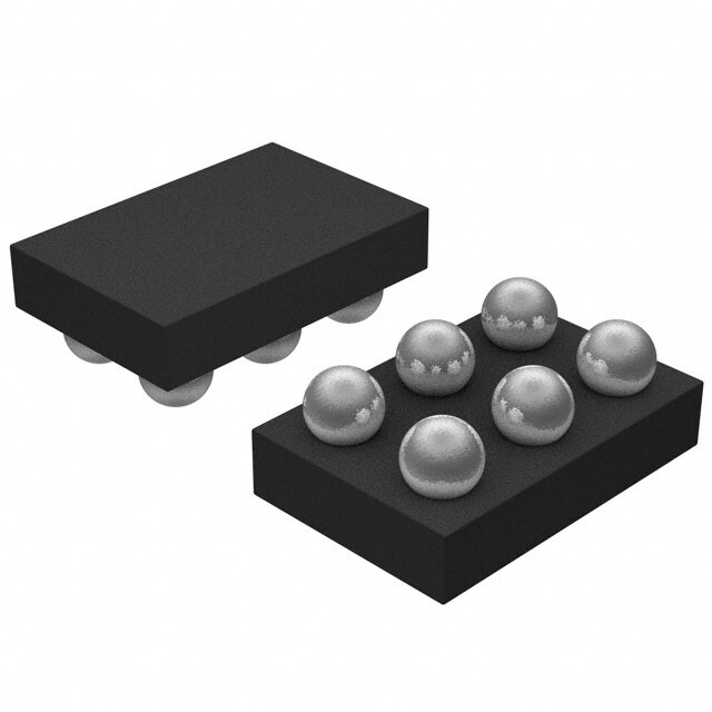
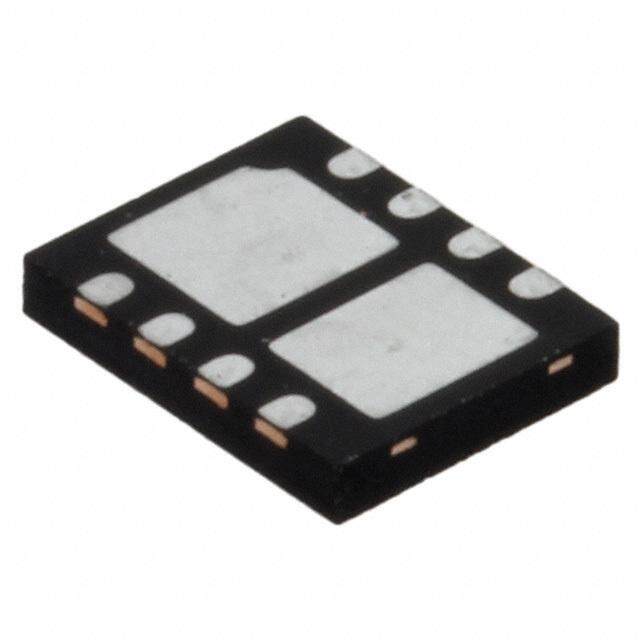
| 产品图片 |
|
| 产品型号 | MCP16301HT-E/CH |
| PWM类型 | 电流模式 |
| rohs | 无铅 / 符合限制有害物质指令(RoHS)规范要求 |
| 产品系列 | - |
| 供应商器件封装 | SOT-23-6 |
| 其它名称 | MCP16301HT-E/CHCT |
| 其它有关文件 | http://www.microchip.com/mymicrochip/filehandler.aspx?ddocname=en554740 |
| 包装 | 剪切带 (CT) |
| 参考设计库 | http://www.digikey.com/rdl/4294959904/4294959903/1317 |
| 同步整流器 | 无 |
| 安装类型 | 表面贴装 |
| 封装/外壳 | SOT-23-6 |
| 工作温度 | -40°C ~ 125°C |
| 应用说明 | |
| 标准包装 | 1 |
| 电压-输入 | 4.7 V ~ 36 V |
| 电压-输出 | 2 V ~ 15 V |
| 电流-输出 | 600mA |
| 类型 | 降压(降压) |
| 输出数 | 1 |
| 输出类型 | 可调式 |
| 配用 | /product-detail/zh/ADM00433/ADM00433-ND/4739288/product-detail/zh/ADM00399/ADM00399-ND/4739287 |
| 频率-开关 | 500kHz |


- 商务部:美国ITC正式对集成电路等产品启动337调查
- 曝三星4nm工艺存在良率问题 高通将骁龙8 Gen1或转产台积电
- 太阳诱电将投资9.5亿元在常州建新厂生产MLCC 预计2023年完工
- 英特尔发布欧洲新工厂建设计划 深化IDM 2.0 战略
- 台积电先进制程称霸业界 有大客户加持明年业绩稳了
- 达到5530亿美元!SIA预计今年全球半导体销售额将创下新高
- 英特尔拟将自动驾驶子公司Mobileye上市 估值或超500亿美元
- 三星加码芯片和SET,合并消费电子和移动部门,撤换高东真等 CEO
- 三星电子宣布重大人事变动 还合并消费电子和移动部门
- 海关总署:前11个月进口集成电路产品价值2.52万亿元 增长14.8%


PDF Datasheet 数据手册内容提取
MCP16301/H High-Voltage Input Integrated Switch Step-Down Regulator Features General Description • Up to 96% Typical Efficiency The MCP16301/H devices are highly integrated, • Input Voltage Range: high-efficiency, fixed-frequency, step-down DC-DC converters in a popular 6-pin SOT-23 package that - 4.0V to 30V (MCP16301) operates from input voltage sources up to 36V. - 4.7V to 36V (MCP16301H) Integrated features include a high-side switch, • Output Voltage Range: 2.0V to 15V fixed-frequency peak current mode control, internal • 2% Output Voltage Accuracy compensation, peak current limit and overtemperature • Qualification: AEC-Q100 Rev G, Grade 1 protection. Minimal external components are (-40°C to +125°C) necessary to develop a complete step-down DC-DC • Integrated N-Channel Buck Switch: 460m converter power supply. • Minimum 600mA Output Current Over All Input High converter efficiency is achieved by integrating the Voltage Range (See Figure2-6 for Maximum current-limited, low-resistance, high-speed N-Channel Output Current vs. V ): IN MOSFET and associated drive circuitry. High - up to 1A output current at 3.3V, 5V and 12V switching frequency minimizes the size of external V , SOT-23 package at +25°C ambient OUT filtering components, resulting in a small solution size. temperature The MCP16301/H devices can supply 600mA of • 500kHz Fixed Frequency continuous current while regulating the output voltage • Adjustable Output Voltage from 2.0V to 15V. An integrated, high-performance • Low Device Shutdown Current peak current mode architecture keeps the output • Peak Current Mode Control voltage tightly regulated, even during input voltage steps and output current transient conditions that are • Internal Compensation common in power systems. • Stable with Ceramic Capacitors The EN input is used to turn the device on and off. • Internal Soft-Start While turned off, only a few micro amps of current are • Cycle-by-Cycle Peak Current Limit consumed from the input for power shedding and load • Undervoltage Lockout (UVLO): 3.5V distribution applications. • Overtemperature Protection Output voltage is set with an external resistor divider. • Available Package: SOT-23-6 The MCP16301/H devices are offered in a space-saving SOT-23-6 surface mount package. Applications • PIC® Microcontroller and dsPIC® Digital Signal Package Type Controller Bias Supply MCP16301/H • 24V Industrial Input DC-DC Conversion 6-Lead SOT-23 • Set-Top Boxes • DSL Cable Modems BOOST 1 6 SW • Automotive • Wall Cube Regulation GND 2 5 VIN • SLA Battery-Powered Devices • AC-DC Digital Control Power Source VFB 3 4 EN • Power Meters • D2 Package Linear Regulator Replacement - See Figure5-2 • Consumer • Medical and Health Care • Distributed Power Supplies 2011-2015 Microchip Technology Inc. DS20005004D-page 1
MCP16301/H Typical Applications 1N4148 CBOOST L1 VOUT VIN Boost 100nF 15µH 3.3V@600mA 4.7Vto36V SW VIN 40V COUT Schottky 2x10µF C IN Diode 10µF EN 31.6k V FB GND 10k 1N4148 CBOOST L1 VOUT VIN Boost 100nF 22µH 5.0V@600mA 6.0Vto36V SW VIN 40V COUT Schottky 2x10µF C IN Diode 10µF EN 52.3k V FB GND 10k 100 90 VOUT = 5.0V 80 %) 70 V = 3.3V OUT ( 60 y c n 50 e V = 12V IN ci 40 i f Ef 30 20 10 0 10 100 1000 I (mA) OUT DS20005004D-page 2 2011-2015 Microchip Technology Inc.
MCP16301/H 1.0 ELECTRICAL † Notice: Stresses above those listed under “Maximum CHARACTERISTICS Ratings” may cause permanent damage to the device. This is a stress rating only and functional operation of the device at those or any other conditions above those Absolute Maximum Ratings † indicated in the operational sections of this specification is not intended. Exposure to maximum V SW...............................................................-0.5V to 40V IN, rating conditions for extended periods may affect BOOST–GND...................................................-0.5V to 46V BOOST–SW Voltage........................................-0.5V to 6.0V device reliability. V Voltage........................................................-0.5V to 6.0V FB EN Voltage.............................................-0.5V to (V +0.3V) IN Output Short-Circuit Current.................................Continuous Power Dissipation .......................................Internally Limited Storage Temperature...................................-65°C to +150°C Ambient Temperature with Power Applied...-40°C to +125°C Operating Junction Temperature..................-40°C to +150°C ESD Protection On All Pins: HBM.................................................................3kV MM..................................................................200V DC CHARACTERISTICS Electrical Characteristics: Unless otherwise indicated, T =+25°C, V =V =12V, V –V =3.3V, A IN EN BOOST SW V =3.3V, I =100mA, L=15µH, C =C =2x10µF X7R ceramic capacitors. OUT OUT OUT IN Boldface specifications apply over the T range of -40oC to +125oC. A Parameters Sym. Min. Typ. Max. Units Conditions Input Voltage V 4 — 30 V Note1 (MCP16301) IN 4.7 — 36 V Note1 (MCP16301H) Feedback Voltage V 0.784 0.800 0.816 V FB Output Voltage Adjust Range V 2.0 — 15.0 V Note2 OUT Feedback Voltage V /V )/V — 0.01 0.1 %/V V =12V to 30V FB FB IN IN Line Regulation Feedback Input Bias Current I -250 ±10 +250 nA FB Undervoltage Lockout Start UVLO — 3.5 4.0 V V Rising (MCP16301) START IN — 3.5 4.7 V V Rising (MCP16301H) IN Undervoltage Lockout Stop UVLO 2.4 3.0 — V V Falling STOP IN Undervoltage Lockout UVLO — 0.5 — V HYS Hysteresis Switching Frequency f 425 500 550 kHz I =200mA SW OUT Maximum Duty Cycle DC 90 95 — % V =5V; V =0.7V; MAX IN FB I =100mA OUT Minimum Duty Cycle DC — 1 — % MIN NMOS Switch On Resistance R — 0.46 — V –V =3.3V DS(ON) BOOST SW NMOS Switch Current Limit I — 1.3 — A V –V =3.3V N(MAX) BOOST SW Quiescent Current I — 2 7.5 mA V =3.3V; Note3 Q BOOST Quiescent Current - Shutdown I — 7 10 µA V =EN=0V Q OUT Maximum Output Current I 600 — — mA Note1 OUT EN Input Logic High V 1.4 — — V IH EN Input Logic Low V — — 0.4 V IL EN Input Leakage Current I — 0.05 1.0 µA V =12V ENLK EN Note 1: The input voltage should be>output voltage+headroom voltage; higher load currents increase the input voltage necessary for regulation. See characterization graphs for typical input to output operating voltage range and UVLO and UVLO limits. START STOP 2: For V <V , V will not remain in regulation. IN OUT OUT 3: V supply is derived from V . BOOST OUT 2011-2015 Microchip Technology Inc. DS20005004D-page 3
MCP16301/H DC CHARACTERISTICS (CONTINUED) Electrical Characteristics: Unless otherwise indicated, T =+25°C, V =V =12V, V –V =3.3V, A IN EN BOOST SW V =3.3V, I =100mA, L=15µH, C =C =2x10µF X7R ceramic capacitors. OUT OUT OUT IN Boldface specifications apply over the T range of -40oC to +125oC. A Parameters Sym. Min. Typ. Max. Units Conditions Soft-Start Time t — 300 — µS EN Low to High, SS 90% of V OUT Thermal Shutdown Die T — 150 — C SD Temperature Die Temperature Hysteresis T — 30 — C SDHYS Note 1: The input voltage should be>output voltage+headroom voltage; higher load currents increase the input voltage necessary for regulation. See characterization graphs for typical input to output operating voltage range and UVLO and UVLO limits. START STOP 2: For V <V , V will not remain in regulation. IN OUT OUT 3: V supply is derived from V . BOOST OUT TEMPERATURE SPECIFICATIONS Electrical Specifications: Unless otherwise indicated, T =+25°C, V =V =12V, V –V =3.3V, A IN EN BOOST SW V =3.3V OUT Parameters Sym. Min. Typ. Max. Units Conditions Temperature Ranges Operating Junction Temperature Range T -40 — +125 °C Steady State J Storage Temperature Range T -65 — +150 °C A Maximum Junction Temperature T — — +150 °C Transient J Package Thermal Resistances Thermal Resistance, 6L-SOT-23 — 190.5 — °C/W EIA/JESD51-3 Standard JA DS20005004D-page 4 2011-2015 Microchip Technology Inc.
MCP16301/H 2.0 TYPICAL PERFORMANCE CURVES Note: The graphs and tables provided following this note are a statistical summary based on a limited number of samples and are provided for informational purposes only. The performance characteristics listed herein are not tested or guaranteed. In some graphs or tables, the data presented may be outside the specified operating range (e.g., outside specified power supply range) and therefore outside the warranted range. Note: Unless otherwise indicated, V =EN=12V, C =C =2X10µF, L=15µH, V =3.3V, I =200mA, IN OUT IN OUT LOAD TA=+25°C. 90 100 VIN= 16V VIN= 6V 80 90 VIN= 30V %)70 VIN=12V %) 80 VIN= 24V cy ( cy ( 70 VOUT= 12.0V cien60 VIN=30V VOUT= 2.0V cien 60 Effi50 Effi 50 40 40 30 30 0 100 200 300 400 500 600 0 100 200 300 400 500 600 IOUT (mA) IOUT(mA) FIGURE 2-1: 2.0V V Efficiency vs. FIGURE 2-4: 12V V Efficiency vs. OUT OUT I . I . OUT OUT 100 100 VIN= 16V 90 VIN= 6V 90 VIN= 30V %) 80 %) 80 VIN= 24V y ( VIN= 12V y ( c 70 c 70 n n Efficie 60 VIN= 30V VOUT= 3.3V Efficie 60 VOUT= 15.0V 50 50 40 40 30 30 0 100 200 300 400 500 600 0 100 200 300 400 500 600 I (mA) I (mA) OUT OUT FIGURE 2-2: 3.3V V Efficiency vs. FIGURE 2-5: 15V V Efficiency vs. OUT OUT I . I . OUT OUT 100 1400 VIN= 6V VOUT = 3.3V 90 1200 cy (%)7800 VVININ== 1320VV A) 1080000 VOUT = 5V VOUT = 12V en m Effici5600 VOUT= 5.0V I (OUT460000 40 200 30 0 0 100 200 300 400 500 600 6 12 18 24 30 36 IOUT(mA) VIN (V) FIGURE 2-3: 5.0V V Efficiency vs. FIGURE 2-6: Maximum Output Current OUT I . vs. V . OUT IN 2011-2015 Microchip Technology Inc. DS20005004D-page 5
MCP16301/H Note: Unless otherwise indicated, V =EN=12V, C =C =2X10µF, L=15µH, V =3.3V, I =200mA, IN OUT IN OUT LOAD TA=+25°C. 5 1800 4 mA)1600 VIN= 30V mA) 3 IVOOUUTT== 0 3 m.3AV VIN= 6V nt Limit (11240000 VIN= 12V I(Q2 VIN= 12V Curre1000 VIN= 6V k 1 VIN= 30V Pea 800 VOUT= 3.3V 0 600 -40 -25 -10 5 20 35 50 65 80 95 110 125 -40 -25 -10 5 20 35 50 65 80 95 110125 Ambient Temperature (°C) Ambient Temperature (°C) FIGURE 2-7: Input Quiescent Current vs. FIGURE 2-10: Peak Current Limit vs. Temperature. Temperature; V =3.3V. OUT 505 510 Hz)459050 VIVOIOUNUT=T= =1 2 230V.03 VmA 459000 TVAD=S =2 51°0C0 mV k y (490 )(cid:58)480 Frequenc444788505 DSON (m446700 g 470 R450 n chi465 440 wit460 430 S 455 420 -40 -20 0 20 40 60 80 100 120 3 3.5 4 4.5 5 Ambient Temperature (°C) Boost Voltage (V) FIGURE 2-8: Switching Frequency vs. FIGURE 2-11: Switch R vs. V DSON BOOST. Temperature; V =3.3V. OUT 95.5 0.802 95.4 VIN= 5V VIN= 12V Cycle (%) 9955..23 IOUT= 200 mA ge (V)00..880001 VIOOUUTT== 1 30.03 VmA uty 95.1 olta0.799 D V um 95 VFB0.798 m 94.9 Maxi 94.8 0.797 94.7 0.796 -40 -25 -10 5 20 35 50 65 80 95 110125 -40 -20 0 20 40 60 80 100 120 Ambient Temperature (°C) Ambient Temperature (°C) FIGURE 2-9: Maximum Duty Cycle vs. FIGURE 2-12: V vs. Temperature; FB Ambient Temperature; V =5.0V. V =3.3V. OUT OUT DS20005004D-page 6 2011-2015 Microchip Technology Inc.
MCP16301/H Note: Unless otherwise indicated, V =EN=12V, C =C =2X10µF, L=15µH, V =3.3V, I =200mA, IN OUT IN OUT LOAD TA=+25°C. 3.80 VOUT = 3.3V 3.70 IOUT = 600 mA 3.60 VIN = 12V 3.50 UVLO Start V20O UmTV =/ DIV 3.40 AC coupled V) 3.30 e ( 3.20 VSW = g 5V/DIV a 3.10 olt 3.00 V 2.90 UVLO Stop 2.80 2.70 IL = 2.60 20mA/DIV 2.50 -40 -25 -10 5 20 35 50 65 80 95 110125 Ambient Temperature (°C) 1µs/DIV FIGURE 2-13: Undervoltage Lockout vs. FIGURE 2-16: Heavy Load Switching Temperature. Waveforms. 0.70 5.00 V) VIN= 12V age (0.65 VIOOUUTT== 1 30.03 VmA e (V)4.70 olt0.60 ag4.40 To Start hold V0.55 ut Volt4.10 s p e n Thr0.50 m I3.80 able 0.45 nimu3.50 To Run En Mi 0.40 3.20 -40 -25 -10 5 20 35 50 65 80 95 110 125 1 10 100 1000 Ambient Temperature (°C) I (mA) OUT FIGURE 2-14: EN Threshold Voltage vs. FIGURE 2-17: Typical Minimum Input Temperature. Voltage vs. Output Current. VOUT VIVOOIUNUT =T = 1= 52 30V. 3mVA VIVOOIUNUT =T = 1= 12 30V.03 VmA 20 mV/DIV AC coupled VSW V2V2VVOO//UUDDTTIIVV 5V/DIV VEN 2V/DIV IL 100mA/DIV 1µs/DIV 110000µµss//DIV FIGURE 2-15: Light Load Switching FIGURE 2-18: Start-Up From Enable. Waveforms. 2011-2015 Microchip Technology Inc. DS20005004D-page 7
MCP16301/H Note: Unless otherwise indicated, V =EN=12V, C =C =2X10µF, L=15µH, V =3.3V, I =200mA, IN OUT IN OUT LOAD TA=+25°C. VOUT = 3.3V IOUT = 100 mA VIN = 12V VOUT 1V/DIV VIN 5V/DIV 100µs/DIV FIGURE 2-19: Start-Up from V IN. VOUT = 3.3V IOUT = 100mA to 600 mA VOUT AC coupled 100mV/DIV IOUT 200mA/DIV 100µs/DIV FIGURE 2-20: Load Transient Response. VOUT = 3.3V IOUT = 100mA VIN = 8V to 12V Step VOUT AC coupled 100mV/DIV VIN 2V/DIV 10µs/DIV FIGURE 2-21: Line Transient Response. DS20005004D-page 8 2011-2015 Microchip Technology Inc.
MCP16301/H 3.0 PIN DESCRIPTIONS The descriptions of the pins are listed in Table3-1. TABLE 3-1: PIN FUNCTION TABLE MCP16301/H Symbol Description SOT-23 1 BOOST Boost voltage that drives the internal NMOS control switch. A bootstrap capacitor is connected between the BOOST and SW pins. 2 GND Ground pin. 3 VFB Output voltage feedback pin. Connect VFB to an external resistor divider to set the output voltage. 4 EN Enable pin. Logic high enables the operation. Do not allow this pin to float. 5 V Input supply voltage pin for power and internal biasing. IN 6 SW Output switch node. This pin connects to the inductor, the freewheeling diode and the bootstrap capacitor. 3.1 Boost Pin (BOOST) 3.5 Power Supply Input Voltage Pin (V ) The high side of the floating supply used to turn the IN integrated N-Channel MOSFET on and off is Connect the input voltage source to V . The input IN connected to the boost pin. source should be decoupled to GND with a 4.7µF-20µF capacitor, depending on the impedance 3.2 Ground Pin (GND) of the source and output current. The input capacitor provides AC current for the power switch and a stable The ground or return pin is used for circuit ground voltage source for the internal device power. This connection. The length of the trace from the input cap capacitor should be connected as close as possible to return, output cap return and GND pin should be made as the V and GND pins. For lighter load applications, a IN short as possible to minimize the noise on the GND pin. 1µFX7R (or X5R, for limited temperature range, -40 to +85°C) ceramic capacitor can be used. 3.3 Feedback Voltage Pin (V ) FB 3.6 Switch Pin (SW) The V pin is used to provide output voltage regulation FB The Switch Node pin is connected internally to the by using a resistor divider. The V voltage will be FB N-Channel switch and externally to the SW node 0.800V typical with the output voltage in regulation. consisting of the inductor and Schottky diode. The SW node can rise very fast as a result of the internal switch 3.4 Enable Pin (EN) turning on. The external Schottky diode should be connected close to the SW node and GND. The EN pin is a logic-level input used to enable or disable device switching and to lower the quiescent current while disabled. A logic high (>1.4V) will enable the regulator output. A logic low (<0.4V) will ensure that the regulator is disabled. 2011-2015 Microchip Technology Inc. DS20005004D-page 9
MCP16301/H NOTES: DS20005004D-page 10 2011-2015 Microchip Technology Inc.
MCP16301/H 4.0 DETAILED DESCRIPTION 4.1.4 ENABLE INPUT Enable input, (EN), is used to enable and disable the 4.1 Device Overview device. If disabled, the MCP16301/H devices consume a minimal current from the input. Once enabled, the The MCP16301/H devices are high-input voltage internal soft start controls the output voltage rate of rise, step-down regulators, capable of supplying 600mA to preventing high-inrush current and output voltage a regulated output voltage from 2.0V to 15V. Internally, overshoot. the trimmed 500kHz oscillator provides a fixed frequency, while the peak current mode control 4.1.5 SOFT START architecture varies the duty cycle for output voltage The internal reference voltage rate of rise is controlled regulation. An internal floating driver is used to turn the during start-up, minimizing the output voltage over- high-side integrated N-Channel MOSFET on and off. shoot and the inrush current. The power for this driver is derived from an external boost capacitor whose energy is supplied from a fixed 4.1.6 UNDERVOLTAGE LOCKOUT voltage ranging from 3.0V to 5.5V, typically the input or output voltage of the converter. For applications with an An integrated Undervoltage Lockout (UVLO) prevents output voltage outside of this range, such as 12V, the the converter from starting until the input voltage is high boost capacitor bias can be derived from the output enough for normal operation. The converter will typically using a simple Zener diode regulator. start at 3.5V and operate down to 3.0V. Hysteresis is added to prevent starting and stopping during start-up, 4.1.1 INTERNAL REFERENCE VOLTAGE as a result of loading the input voltage source. (V ) REF 4.1.7 OVERTEMPERATURE An integrated precise 0.8V reference combined with an PROTECTION external resistor divider sets the desired converter output voltage. The resistor divider range can vary Overtemperature protection limits the silicon die without affecting the control system gain. High-value temperature to +150°C by turning the converter off. The resistors consume less current, but are more normal switching resumes at +120°C. susceptible to noise. 4.1.2 INTERNAL COMPENSATION All control system components necessary for stable operation over the entire device operating range are integrated, including the error amplifier and inductor current slope compensation. To add the proper amount of slope compensation, the inductor value changes along with the output voltage (see Table5-1). 4.1.3 EXTERNAL COMPONENTS External components consist of: • input capacitor • output filter (inductor and capacitor) • freewheeling diode • boost capacitor • boost blocking diode • resistor divider. The selection of the external inductor, output capacitor, input capacitor and freewheeling diode is dependent upon the output voltage and the maximum output current. 2011-2015 Microchip Technology Inc. DS20005004D-page 11
MCP16301/H V IN CIN RBEGF VREG Boost Boost Diode Pre- BOOST charge VOUT SS OTEMP V C REF 500kHz OSC BOOST V OUT RTOP + S HS SW FB Amp - Drive Schottky - Comp PWM Diode + Latch COUT RBOT RCOMP Precharge R Overtemp + CS V C + REF COMP R SENSE + EN SHDN all blocks Slope - GND Comp GND FIGURE 4-1: MCP16301/H Block Diagram. 4.2 Functional Description chopped input voltage or SW node voltage is equal to the output voltage, while the average of the inductor 4.2.1 STEP-DOWN OR BUCK current is equal to the output current. CONVERTER I The MCP16301/H devices are non-synchronous L V step-down or buck converters, capable of stepping SW OUT input voltages ranging from 4V to 30V (MCP16301) or L + Schottky C 36V (MCP16301H) down to 2.0V to 15V for VIN>VOUT. VIN - Diode OUT The integrated high-side switch is used to chop or modulate the input voltage using a controlled duty cycle for output voltage regulation. High efficiency is achieved by using a low-resistance switch, low forward drop diode, low equivalent series resistance (ESR), an IL IOUT inductor and a capacitor. When the switch is turned on, 0 a DC voltage is applied to the inductor (V –V ), V IN OUT IN resulting in a positive linear ramp of inductor current. SW V When the switch turns off, the applied inductor voltage OUT on off on off on is equal to -V , resulting in a negative linear ramp of OUT Continuous Inductor Current Mode inductor current (ignoring the forward drop of the Schottky diode). For steady-state, continuous inductor current I operation, the positive inductor current ramp must L I OUT equal the negative current ramp in magnitude. While 0 operating in steady state, the switch duty cycle must be VIN equal to the relationship of VOUT/VIN for constant SW output voltage regulation, under the condition that the on off on off on inductor current is continuous or never reaches zero. Discontinuous Inductor Current Mode For discontinuous inductor current operation, the steady-state duty cycle will be less than V /V to FIGURE 4-2: Step-Down Converter. OUT IN maintain voltage regulation. The average of the DS20005004D-page 12 2011-2015 Microchip Technology Inc.
MCP16301/H 4.2.2 PEAK CURRENT MODE CONTROL 4.2.4 HIGH-SIDE DRIVE The MCP16301/H devices integrate a Peak Current The MCP16301/H devices feature an integrated Mode Control architecture, resulting in superior AC high-side N-Channel MOSFET for high-efficiency regulation while minimizing the number of voltage loop step-down power conversion. An N-Channel MOSFET compensation components, and their size, for is used for its low resistance and size (instead of a integration. Peak Current Mode Control takes a small P-Channel MOSFET). The N-Channel MOSFET gate portion of the inductor current, replicates it, and must be driven above its source to fully turn on the compares this replicated current sense signal to the transistor. A gate-drive voltage above the input is output of the integrated error voltage. In practice, the necessary to turn on the high-side N-Channel. The inductor current and the internal switch current are high-side drive voltage should be between 3.0V and equal during the switch-on time. By adding this peak 5.5V. The N-Channel source is connected to the current sense to the system control, the step-down inductor and Schottky diode, or switch node. power train system is reduced from a 2nd order to a 1st When the switch is off, the inductor current flows order. This reduces the system complexity and through the Schottky diode, providing a path to increases its dynamic performance. recharge the boost cap from the boost voltage source: For Pulse-Width Modulation (PWM) duty cycles that typically the output voltage for 3.0V to 5.0V output exceed 50%, the control system can become bimodal applications. A boost-blocking diode is used to prevent where a wide pulse followed by a short pulse repeats current flow from the boost cap back into the output instead of the desired fixed pulse width. To prevent this during the internal switch-on time. Prior to start-up, the mode of operation, an internal compensating ramp is boost cap has no stored charge to drive the switch. An summed into the current shown in Figure4-1. internal regulator is used to precharge the boost cap. Once precharged, the switch is turned on and the 4.2.3 PULSE-WIDTH MODULATION inductor current flows. When the switch turns off, the (PWM) inductor current free-wheels through the Schottky The internal oscillator periodically starts the switching diode, providing a path to recharge the boost cap. period, which, for MCP16301, occurs every 2µs or Worst-case conditions for recharge occur when the 500kHz. With the integrated switch turned on, the switch turns on for a very short duty cycle at light load, inductor current ramps up until the sum of the current limiting the inductor current ramp. In this case, there is sense and slope compensation ramp exceeds the a small amount of time for the boost capacitor to integrated error amplifier output. The error amplifier recharge. For high input voltages there is enough pre- output slews up or down to increase or decrease the charge current to replace the boost cap charge. For inductor peak current feeding into the output LC filter. If input voltages above 5.5V typical, the MCP16301/H the regulated output voltage is lower than its target, the devices will regulate the output voltage with no load. inverting error amplifier output rises. This results in an After starting, the MCP16301/H devices will regulate increase in the inductor current to correct the errors in the output voltage until the input voltage decreases the output voltage. below 4V. See Figure2-17 for device range of opera- tion over input voltage, output voltage and load. The fixed-frequency duty cycle is terminated when the sensed inductor peak current, summed with the 4.2.5 ALTERNATIVE BOOST BIAS internal slope compensation, exceeds the output voltage of the error amplifier. The PWM latch is reset by For 3.0V to 5.0V output voltage applications, the boost turning off the internal switch and preventing it from supply is typically the output voltage. For applications turning on until the beginning of the next cycle. An with 3.0V<VOUT<5.0V, an alternative boost supply overtemperature signal, or boost cap undervoltage, can be used. can also reset the PWM latch to asynchronously Alternative boost supplies can be from the input, input terminate the cycle. derived, output derived or an auxiliary system voltage. For low voltage output applications with unregulated input voltage, a shunt regulator derived from the input can be used to derive the boost supply. For applications with high output voltage or regulated high input voltage, a series regulator can be used to derive the boost supply. 2011-2015 Microchip Technology Inc. DS20005004D-page 13
MCP16301/H Boost Diode C1 V =5.1V Z BOOST RSH CB EN L V OUT VIN MCP16301/H SW 2V 12V VIN COUT FW Diode R C TOP IN FB GND R BOT 3.0V to 5.5V External Supply Boost Diode BOOST C B EN L V OUT VIN MCP16301/H SW 2V 12V VIN COUT FW Diode R C TOP IN FB GND R BOT FIGURE 4-3: Shunt and External Boost Supply. Shunt Boost Supply Regulation is used for low-output I for 3.3V Boost Supply=0.6mA BOOST_TYP voltage converters operating from a wide ranging input I for 5.0V Boost Supply=0.8mA BOOST_TYP source. A regulated 3.0V to 5.5V supply is needed to provide high-side drive bias. The shunt uses a Zener EQUATION 4-1: BOOST CURRENT diode to clamp the voltage within the 3.0V to 5.5V range using the resistance shown in Figure4-3. I = I 1.5mA BOOST BOOST_TYP To calculate the shunt resistance, the boost drive current can be estimated using Equation4-1. DS20005004D-page 14 2011-2015 Microchip Technology Inc.
MCP16301/H To calculate the shunt resistance, the maximum I BOOST and I currents are used at the minimum input voltage Z (Equation4-2). EQUATION 4-2: SHUNT RESISTANCE V –V INMIN Z R = ------------------------------ SH I + I Boost Z V and I can be found on the Zener diode Z Z manufacturer’s data sheet (typical I =1mA). Z Boost Diode V =7.5V Z BOOST C B EN L V OUT VIN MCP16301/H SW 12V 15V to 36V VIN COUT FW Diode R C TOP IN FB GND R BOT Boost Diode BOOST VZ=7.5V CB EN L V OUT VIN MCP16301/H SW 2V 12V VIN COUT FW Diode R C TOP IN FB GND R BOT FIGURE 4-4: Series Regulator Boost Supply. Series regulator applications use a Zener diode to drop the excess voltage. The series regulator bias source can be input or output voltage derived, as shown in Figure4-4. For proper circuit operation, the boost supply must remain between 3.0V and 5.5V at all times. 2011-2015 Microchip Technology Inc. DS20005004D-page 15
MCP16301/H NOTES: DS20005004D-page 16 2011-2015 Microchip Technology Inc.
MCP16301/H 5.0 APPLICATION INFORMATION 5.3 General Design Equations The step-down converter duty cycle can be estimated 5.1 Typical Applications using Equation5-2 while operating in Continuous Inductor Current mode. This equation also counts the The MCP16301/H step-down converters operate over forward drop of the freewheeling diode and internal a wide input voltage range, up to 36V maximum. N-Channel MOSFET switch voltage drop. As the load Typical applications include generating a bias or V DD voltage for the PIC® microcontroller product line, digital current increases, the switch voltage drop and diode voltage drop increase, requiring a larger PWM duty control system bias supply for AC-DC converters, 24V cycle to maintain the output voltage regulation. Switch industrial input and similar applications. voltage drop is estimated by multiplying the switch current times the switch resistance or R . 5.2 Adjustable Output Voltage DSON Calculations EQUATION 5-2: CONTINUOUS INDUCTOR To calculate the resistor divider values for the CURRENT DUTY CYCLE MCP16301/H devices, Equation5-1 can be used. V +V R is connected to V , R is connected to GND OUT Diode TOP OUT BOT D = ------------------------------------------------------- and both are connected to the V input pin. V –I R FB IN SW DSON EQUATION 5-1: The MCP16301/H devices feature an integrated slope V compensation to prevent the bimodal operation of the OUT R = R ------------- –1 PWM duty cycle. Internally, half of the inductor current TOP BOT V FB down slope is summed with the internal current sense signal. For the proper amount of slope compensation, it is recommended to keep the inductor down-slope EXAMPLE 5-1: current constant by varying the inductance with V , OUT where K=0.22V/µH. V = 3.3V OUT VFB = 0.8V EQUATION 5-3: R = 10k BOT RTOP = 31.25k (standard value=31.6k) K = V L OUT V = 3.328V (using standard value) OUT For V =3.3V, an inductance of 15µH is OUT EXAMPLE 5-2: recommended. VOUT = 5.0V TABLE 5-1: RECOMMENDED INDUCTOR V = 0.8V VALUES FB RBOT = 10k VOUT K LSTANDARD R = 52.5k (standard value = 52.3k) TOP 2.0V 0.20 10µH V = 4.98V (using standard value) OUT 3.3V 0.22 15µH 5.0V 0.23 22µH The transconductance error amplifier gain is controlled 12V 0.21 56µH by its internal impedance. The external divider resistors have no effect on system gain, so a wide range of 15V 0.22 68µH values can be used. A 10k resistor is recommended as a good trade-off for quiescent current and noise immunity. 2011-2015 Microchip Technology Inc. DS20005004D-page 17
MCP16301/H 5.4 Input Capacitor Selection 5.6 Inductor Selection The step-down converter input capacitor must filter the The MCP16301/H devices are designed to be used high input ripple current as a result of pulsing or with small surface mount inductors. Several chopping the input voltage. The input voltage pin of the specifications should be considered prior to selecting MCP16301/H devices is used to supply voltage for the an inductor. To optimize system performance, the power train and as a source for internal bias. A low inductance value is determined by the output voltage equivalent series resistance (ESR), preferably a (Table5-1) so the inductor ripple current is somewhat ceramic capacitor, is recommended. The necessary constant over the output voltage range. capacitance is dependent upon the maximum load current and source impedance. Three capacitor EQUATION 5-4: INDUCTOR RIPPLE parameters to keep in mind are the voltage rating, CURRENT equivalent series resistance and the temperature V rating. For wide temperature range applications, a = ----L--t multi-layer X7R dielectric is mandatory, while for IL L ON applications with limited temperature range, a multi-layer X5R dielectric is acceptable. Typically, input EXAMPLE 5-3: capacitance between 4.7µF and 10µF is sufficient for most applications. For applications with 100mA to V = 12V IN 200mA load, a 1µF X7R capacitor can be used, V = 3.3V depending on the input source and its impedance. OUT I = 600mA OUT The input capacitor voltage rating should be a minimum of V plus margin. Table5-2 contains the IN recommended range for the input capacitor value. EQUATION 5-5: INDUCTOR PEAK CURRENT 5.5 Output Capacitor Selection I L The output capacitor helps in providing a stable output I = -------- + I LPK 2 OUT voltage during sudden load transients, and reduces the output voltage ripple. As with the input capacitor, X5R Inductor ripple current=319mA and X7R ceramic capacitors are well suited for this Inductor peak current=760mA application. The MCP16301/H devices are internally compensated, so the output capacitance range is limited. See An inductor saturation rating minimum of 760mA is Table5-2 for the recommended output capacitor range. recommended. Low ESR inductors result in higher The amount and type of output capacitance and system efficiency. A trade-off between size, cost and equivalent series resistance will have a significant efficiency is made to achieve the desired results. effect on the output ripple voltage and system stability. The range of the output capacitance is limited due to the integrated compensation of the MCP16301/H devices. The output voltage capacitor voltage rating should be a minimum of V , plus margin. OUT Table5-2 contains the recommended range for the input and output capacitor value: TABLE 5-2: CAPACITOR VALUE RANGE Parameter Min Max C 2.2µF none IN C 20µF none OUT DS20005004D-page 18 2011-2015 Microchip Technology Inc.
MCP16301/H 5.7 Freewheeling Diode TABLE 5-3: MCP16301/H RECOMMENDED 3.3V INDUCTORS The freewheeling diode creates a path for inductor Part Number Value(µH) DCR () (A)ISAT W(SmxiLzmxe)H cacisuuv rerarrree annfgutte naf cltod tdiwiooun dtay ef ot cecfy ruc trthlrheeee ( n Dftion )ir.ts ewT rdahnereadp le esfdnfwirdcoiietpecn nhtac iunysp d oto uf snrthpn oeeeu edctd opo nufofvt. f e lTortthaheeder Coilcraft® freewheeling diode. A low forward drop Schottky diode ME3220 15 0.52 0.90 3.2x2.5x2.0 is recommended. The current rating and voltage rating of the diode is application dependent. The diode LPS4414 15 0.440 0.92 4.3x4.3x1.4 voltage rating should be a minimum of V , plus margin. IN LPS6235 15 0.125 2.00 6.0x6.0x3.5 For example, a diode rating of 40V should be used for MSS6132 15 0.135 1.56 6.1x6.1x3.2 an application with a maximum input of 30V. The MSS7341 15 0.057 1.78 7.3x7.3x4.1 average diode current can be calculated using Equation5-6. ME3220 15 0.520 0.8 2.8x3.2x2.0 LPS3015 15 0.700 0.61 3.0x3.0x1.4 EQUATION 5-6: DIODE AVERAGE Würth Elektronik Group® CURRENT 744025 15 0.400 0.900 2.8x2.8x2.8 I = 1–DI 744031 15 0.255 0.450 3.8x3.8x1.65 D1AVG OUT 744042 15 0.175 0.75 4.8x4.8x1.8 Coiltronics® EXAMPLE 5-4: SD12 15 0.48 0.692 5.2x5.2x1.2 I = 0.5A OUT SD18 15 0.266 0.831 5.2x5.2x1.8 V = 15V IN SD20 15 0.193 0.718 5.2x5.2x2.0 V = 5V OUT SD3118 15 0.51 0.75 3.2x3.2x1.8 D = 5/15 SD52 15 0.189 0.88 5.2x5.5.2.0 I = 333mA D1AVG Sumida® Corporation CDPH4D19F 15 0.075 0.66 5.2x5.2x2.0 A 0.5A to 1A diode is recommended. CDRH3D161H 15 0.328 0.65 4.0x4.0x1.8 TABLE 5-4: FREEWHEELING DIODES TDK-EPC® Part VLF30251 15 0.5 0.47 2.5x3.0x1.2 App Manufacturer Rating Number VLF4012A 15 0.46 0.63 3.5x3.7x1.2 12 V Diodes DFLS120L-7 20V, 1A IN VLF5014A 15 0.28 0.97 4.5x4.7x1.4 600mA Incorporated® B82462G4332M 15 0.097 1.05 6x6x2.2 24 V Diodes B0540Ws-7 40V, 0.5A IN 100mA Incorporated 18 V Diodes B130L-13-F 30V, 1A IN 600mA Incorporated 5.8 Boost Diode The boost diode is used to provide a charging path from the low-voltage gate drive source, while the switch node is low. The boost diode blocks the high voltage of the switch node from feeding back into the output voltage when the switch is turned on, forcing the switch node high. A standard 1N4148 ultra-fast diode is recommended for its recovery speed, high voltage blocking capability, availability and cost. The voltage rating required for the boost diode is V . IN For low boost voltage applications, a small Schottky diode with the appropriately rated voltage can be used to lower the forward drop, increasing the boost supply for gate drive. 2011-2015 Microchip Technology Inc. DS20005004D-page 19
MCP16301/H 5.9 Boost Capacitor EXAMPLE 5-5: The boost capacitor is used to supply current for the V = 10V internal high-side drive circuitry that is above the input IN V = 5V voltage. The boost capacitor must store enough energy OUT to completely drive the high-side switch on and off. A I = 0.4A OUT 0.1µF X5R or X7R capacitor is recommended for all Efficiency = 90% applications. The boost capacitor maximum voltage is Total System Dissipation = 222mW 5.5V, so a 6.3V or 10V rated capacitor is recommended. In case of a noise-sensitive application, LESR = 0.15 an additional resistor in series with the boost capacitor, P = 24mW L that will reduce the high-frequency noise associated Diode VF = 0.50 with switching power supplies, can be added. A typical D = 50% value for the resistor is 82. P = 125mW Diode 5.10 Thermal Calculations MCP16301/H internal power dissipation estimate: The MCP16301/H devices are available in a SOT-23-6 package. By calculating the power dissipation and PDIS-PL-PDIODE=73mW applying the package thermal resistance ( ), the JA junction temperature is estimated. The maximum = 198°C/W continuous junction temperature rating for the JA Estimated Junction = +14.5°C MCP16301/H devices is +125°C. Temperature Rise To quickly estimate the internal power dissipation for the switching step-down regulator, an empirical calculation using measured efficiency can be used. 5.11 PCB Layout Information Given the measured efficiency, the internal power dissipation is estimated by Equation5-7. This power Good printed circuit board layout techniques are dissipation includes all internal and external important to any switching circuitry, and switching component losses. For a quick internal estimate, power supplies are no different. When wiring the subtract the estimated Schottky diode loss and inductor switching high-current paths, short and wide traces ESR loss from the P calculation in Equation5-7. should be used. Therefore, it is important that the input DIS and output capacitors be placed as close as possible to EQUATION 5-7: TOTAL POWER the MCP16301/H devices to minimize the loop area. DISSIPATION ESTIMATE The feedback resistors and feedback signal should be V I routed away from the switching node and the switching OUT OUT ------------------------------- –V I = P current loop. When possible, ground planes and traces Efficiency OUT OUT Dis should be used to help shield the feedback signal and minimize noise and magnetic interference. The difference between the first term, input power, and A good MCP16301/H layout starts with C placement. the second term, power delivered, is the total system IN C supplies current to the input of the circuit when the power dissipation. The freewheeling Schottky diode IN switch is turned on. In addition to supplying losses are determined by calculating the average diode high-frequency switch current, C also provides a current and multiplying by the diode forward drop. The IN inductor losses are estimated by P =I 2xL . stable voltage source for the internal MCP16301/H L OUT ESR circuitry. Unstable PWM operation can result if there are excessive transients or ringing on the V pin of the EQUATION 5-8: DIODE POWER IN MCP16301/H devices. In Figure5-1, C is placed DISSIPATION ESTIMATE IN close to pin5. A ground plane on the bottom of the board provides a low resistive and inductive path for P = V 1–DI Diode F OUT the return current. The next priority in placement is the freewheeling current loop formed by D1, C and L, OUT while strategically placing C return close to C OUT IN return. Next, C and D should be placed between the B B boost pin and the switch node pin SW. This leaves space close to the V pin of the MCP16301/H devices FB to place R and R . R and R are routed TOP BOT TOP BOT away from the Switch node so noise is not coupled into the high-impedance V input. FB DS20005004D-page 20 2011-2015 Microchip Technology Inc.
MCP16301/H Bottom Plane is GND Bottom Trace RBOTRTOP 10Ohm MCP16301/H EN 1CB DB R EN V IN V OUT D1 L 2xC IN GND C OUT C GND OUT DB 1 4 BOOST EN CB VOUT REN L 3.3V 6 VIN MCP16301/H SW 5 VIN COUT 10Ohm 4V to 30V D1 C IN R TOP 3 FB GND 2 R BOT Component Value C 10µF IN C 2x10µF OUT L 15µH R 31.6k TOP R 10k BOT D1 B140 DB 1N4148 *Note: The 10 resistor is used with network analyzer, to measure C 100nF system gain and phase. B FIGURE 5-1: MCP16301/H SOT-23-6 Recommended Layout, 600mA Design. 2011-2015 Microchip Technology Inc. DS20005004D-page 21
MCP16301/H Bottom Plane is GND MCP16301/H R BOT R TOP D VIN B VOUT C B R EN L C IN GND GND C OUT D1 GND D B 1 4 BOOST EN C B V REN L 3O.3UVT 6 VIN 5 MCP16301/H SW VIN COUT 4V to 30V D1 C IN R TOP 3 FB GND 2 Component Value R BOT C 1µF IN C 10µF OUT L 15µH R 31.6k TOP R 10k BOT D1 PD3S130 C 100nF B R 1M EN FIGURE 5-2: MCP16301/H SOT-23-6 D2 Recommended Layout, 200mA Design. DS20005004D-page 22 2011-2015 Microchip Technology Inc.
MCP16301/H 6.0 TYPICAL APPLICATION CIRCUITS Boost Diode BOOST C B EN L V OUT VIN MCP16301/H SW 3.3V 6V to 30V VIN COUT FW Diode R C TOP IN FB GND R BOT Component Value Manufacturer Part Number Comment C 2x4.7µF Taiyo Yuden® UMK325B7475KM-T Cap. 4.7µF 50V Ceramic X7R 1210 10% IN Co., Ltd. C 2x10µF Taiyo Yuden JMK212B7106KG-T Cap. 10µF 6.3V Ceramic X7R 0805 10% OUT Co., Ltd. L 15µH Coilcraft® MSS6132-153ML MSS6132 15µH Shielded Power Inductor R 31.6k Panasonic®-ECG ERJ-3EKF3162V Res. 31.6k 1/10W 1% 0603 SMD TOP R 10k Panasonic-ECG ERJ-3EKF1002V Res. 10.0k 1/10W 1% 0603 SMD BOT FW Diode B140 Diodes B140-13-F Diode Schottky 40V 1A SMA Incorporated® Boost Diode 1N4148 Diodes 1N4448WS-7-F Diode Switch 75V 200mW SOD-323 Incorporated C 100nF AVX® Corporation 0603YC104KAT2A Cap. 0.1µF 16V Ceramic X7R 0603 10% B FIGURE 6-1: Typical Application 30V V to 3.3V V . IN OUT 2011-2015 Microchip Technology Inc. DS20005004D-page 23
MCP16301/H Boost Diode BOOST C B D Z EN L V OUT VIN MCP16301/H SW 12V 15V to 30V VIN COUT FW Diode R C TOP IN FB GND R BOT Component Value Manufacturer Part Number Comment C 2x4.7µF Taiyo Yuden® UMK325B7475KM-T Cap. 4.7uF 50V Ceramic X7R 1210 10% IN Co., Ltd. C 2x10µF Taiyo Yuden JMK212B7106KG-T Cap. Ceramic 10µF 25V X7R 10% 1206 OUT Co., Ltd. L 56µH Coilcraft® MSS6132-153ML MSS7341 56µH Shielded Power Inductor R 140k Panasonic®-ECG ERJ-3EKF3162V Res. 140k 1/10W 1% 0603 SMD TOP R 10k Panasonic-ECG ERJ-3EKF1002V Res. 10.0k 1/10W 1% 0603 SMD BOT FW Diode B140 Diodes B140-13-F Diode Schottky 40V 1A SMA Incorporated® Boost Diode 1N4148 Diodes 1N4448WS-7-F Diode Switch 75V 200mW SOD-323 Incorporated C 100nF AVX® Corporation 0603YC104KAT2A Cap. 0.1µF 16V Ceramic X7R 0603 10% B D 7.5V Zener Diodes MMSZ5236BS-7-F Diode Zener 7.5V 200mW SOD-323 Z Incorporated FIGURE 6-2: Typical Application 15V–30V Input; 12V Output. DS20005004D-page 24 2011-2015 Microchip Technology Inc.
MCP16301/H D Z Boost Diode BOOST C B EN L V OUT VIN MCP16301/H SW 2V 12V V C IN OUT FW Diode R C TOP IN FB GND R BOT Component Value Manufacturer Part Number Comment C 10µF Taiyo Yuden® EMK316B7106KL-TD Cap. Ceramic 10µF 16V X7R 10% 1206 IN Co., Ltd. C 22µF Taiyo Yuden JMK316B7226ML-T Cap. Ceramic 22µF 6.3V X7R 1206 OUT Co., Ltd. L 10µH Coilcraft® MSS4020-103ML 10µH Shielded Power Inductor R 15k Panasonic®-ECG ERJ-3EKF1502V Res. 15.0k 1/10W 1% 0603 SMD TOP R 10k Panasonic-ECG ERJ-3EKF1002V Res. 10.0k 1/10W 1% 0603 SMD BOT FW Diode PD3S Diodes PD3S120L-7 Diode Schottky 1A 20V POWERDI323 Incorporated® Boost Diode 1N4148 Diodes 1N4448WS-7-F Diode Switch 75V 200mW SOD-323 Incorporated C 100nF AVX® Corporation 0603YC104KAT2A Cap. 0.1µF 16V Ceramic X7R 0603 10% B D 7.5V Zener Diodes MMSZ5236BS-7-F Diode Zener 7.5V 200mW SOD-323 Z Incorporated FIGURE 6-3: Typical Application 12V Input; 2V Output at 600mA. 2011-2015 Microchip Technology Inc. DS20005004D-page 25
MCP16301/H Boost Diode CZ DZ BOOST R Z C B EN L V OUT VIN MCP16301/H SW 2.5V 10V to 16V VIN COUT FW Diode R CIN TOP FB GND R BOT Component Value Manufacturer Part Number Comment C 10µF Taiyo Yuden® TMK316B7106KL-TD Cap. Ceramic 10µF 25V X7R 10% 1206 IN Co., Ltd. C 22µF Taiyo Yuden JMK316B7226ML-T Cap. Ceramic 22µF 6.3V X7R 1206 OUT Co., Ltd. L 12µH Coilcraft® LPS4414-123MLB LPS4414 12µH Shielded Power Inductor R 21.5k Panasonic®-ECG ERJ-3EKF2152V Res. 21.5k 1/10W 1% 0603 SMD TOP R 10k Panasonic-ECG ERJ-3EKF1002V Res. 10.0k 1/10W 1% 0603 SMD BOT FW Diode DFLS120 Diodes DFLS120L-7 Diode Schottky 20V 1A POWERDI123 Incorporated® Boost Diode 1N4148 Diodes 1N4448WS-7-F Diode Switch 75V 200mW SOD-323 Incorporated C 100nF AVX® Corporation 0603YC104KAT2A Cap. 0.1µF 16V Ceramic X7R 0603 10% B D 7.5V Zener Diodes MMSZ5236BS-7-F Diode Zener 7.5V 200mW SOD-323 Z Incorporated C 1µF Taiyo Yuden LMK107B7105KA-T Cap. Ceramic 1.0µF 10V X7R 0603 Z Co., Ltd. R 1k Panasonic-ECG ERJ-8ENF1001V Res. 1.00k 1/4W 1% 1206 SMD Z FIGURE 6-4: Typical Application 10V to 16V V to 2.5V V . IN OUT DS20005004D-page 26 2011-2015 Microchip Technology Inc.
MCP16301/H Boost Diode EN BOOST C B R EN L V OUT VIN MCP16301/H SW 3.3V 4V to 30V V C IN OUT FW Diode R C TOP IN FB GND R BOT Component Value Manufacturer Part Number Comment C 1µF Taiyo Yuden® GMK212B7105KG-T Cap. Ceramic 1.0µF 35V X7R 0805 IN Co., Ltd. C 10µF Taiyo Yuden JMK107BJ106MA-T Cap. Ceramic 10µF 6.3V X5R 0603 OUT Co., Ltd. L 15µH Coilcraft® LPS3015-153MLB Inductor Power 15µH 0.61A SMD R 31.6k Panasonic®-ECG ERJ-2RKF3162X Res. 31.6k 1/10W 1% 0402 SMD TOP R 10k Panasonic-ECG ERJ-3EKF1002V Res. 10.0k 1/10W 1% 0603 SMD BOT FW Diode B0540 Diodes B0540WS-7 Diode Schottky 0.5A 40V SOD323 Incorporated® Boost Diode 1N4148 Diodes 1N4448WS-7-F Diode Switch 75V 200mW SOD-323 Incorporated C 100nF TDK® Corporation C1005X5R0J104M Cap. Ceramic 0.10µF 6.3V X5R 0402 B R 10M Panasonic-ECG ERJ-2RKF1004X Res. 1.00M 1/10W 1% 0402 SMD EN FIGURE 6-5: Typical Application 4V to 30V V to 3.3V V at 150mA. IN OUT 2011-2015 Microchip Technology Inc. DS20005004D-page 27
MCP16301/H NOTES: DS20005004D-page 28 2011-2015 Microchip Technology Inc.
MCP16301/H 7.0 PACKAGING INFORMATION 7.1 Package Marking Information 6-Lead SOT-23 Example Part Number Code MCP16301T-I/CHY HTNN HT25 MCP16301T-E/CH JYNN MCP16301HT-E/CH AAANY MCP16301HT-I/CH AAAPY Legend: XX...X Customer-specific information Y Year code (last digit of calendar year) YY Year code (last 2 digits of calendar year) WW Week code (week of January 1 is week ‘01’) NNN Alphanumeric traceability code e3 Pb-free JEDEC® designator for Matte Tin (Sn) * This package is Pb-free. The Pb-free JEDEC designator ( e 3 ) can be found on the outer packaging for this package. Note: In the event the full Microchip part number cannot be marked on one line, it will be carried over to the next line, thus limiting the number of available characters for customer-specific information. 2011-2015 Microchip Technology Inc. DS20005004D-page 29
MCP16301/H (cid:2)(cid:3)(cid:4)(cid:5)(cid:6)(cid:7)(cid:8)(cid:9)(cid:10)(cid:6)(cid:11)(cid:12)(cid:13)(cid:14)(cid:8)(cid:15)(cid:16)(cid:6)(cid:10)(cid:10)(cid:8)(cid:17)(cid:18)(cid:12)(cid:10)(cid:13)(cid:19)(cid:5)(cid:8)(cid:20)(cid:21)(cid:6)(cid:19)(cid:11)(cid:13)(cid:11)(cid:12)(cid:22)(cid:21)(cid:8)(cid:23)(cid:24)(cid:25)(cid:26)(cid:8)(cid:27)(cid:15)(cid:17)(cid:20)(cid:3)(cid:28)(cid:29)(cid:30) (cid:31)(cid:22)(cid:12)(cid:5) /(cid:23)(cid:22)(cid:14)$(cid:24)(cid:13)(cid:14) (cid:23)!$(cid:14)(cid:21)%(cid:22)(cid:22)(cid:13)(cid:26)$(cid:14)(cid:10)(cid:11)(cid:21)0(cid:11)(cid:12)(cid:13)(cid:14)"(cid:22)(cid:11).(cid:20)(cid:26)(cid:12)!1(cid:14)(cid:10)(cid:27)(cid:13)(cid:11)!(cid:13)(cid:14)!(cid:13)(cid:13)(cid:14)$(cid:24)(cid:13)(cid:14)(cid:19)(cid:20)(cid:21)(cid:22)(cid:23)(cid:21)(cid:24)(cid:20)(cid:10)(cid:14)2(cid:11)(cid:21)0(cid:11)(cid:12)(cid:20)(cid:26)(cid:12)(cid:14)(cid:3)(cid:10)(cid:13)(cid:21)(cid:20)&(cid:20)(cid:21)(cid:11)$(cid:20)(cid:23)(cid:26)(cid:14)(cid:27)(cid:23)(cid:21)(cid:11)$(cid:13)"(cid:14)(cid:11)$(cid:14) (cid:24)$$(cid:10),33...(cid:30) (cid:20)(cid:21)(cid:22)(cid:23)(cid:21)(cid:24)(cid:20)(cid:10)(cid:30)(cid:21)(cid:23) 3(cid:10)(cid:11)(cid:21)0(cid:11)(cid:12)(cid:20)(cid:26)(cid:12) b N 4 E E1 PIN1IDBY LASERMARK 1 2 3 e e1 D A A2 c φ L A1 L1 4(cid:26)(cid:20)$! (cid:19)(cid:29)55(cid:29)(cid:19)#(cid:25)#(cid:8)(cid:3) (cid:2)(cid:20) (cid:13)(cid:26)!(cid:20)(cid:23)(cid:26)(cid:14)5(cid:20) (cid:20)$! (cid:19)(cid:29)6 67(cid:19) (cid:19)(cid:7)8 6% 9(cid:13)(cid:22)(cid:14)(cid:23)&(cid:14)2(cid:20)(cid:26)! 6 (cid:16) 2(cid:20)$(cid:21)(cid:24) (cid:13) (cid:4)(cid:30)(cid:6))(cid:14)*(cid:3)+ 7%$!(cid:20)"(cid:13)(cid:14)5(cid:13)(cid:11)"(cid:14)2(cid:20)$(cid:21)(cid:24) (cid:13)(cid:31) (cid:31)(cid:30)(cid:6)(cid:4)(cid:14)*(cid:3)+ 7-(cid:13)(cid:22)(cid:11)(cid:27)(cid:27)(cid:14):(cid:13)(cid:20)(cid:12)(cid:24)$ (cid:7) (cid:4)(cid:30)(cid:6)(cid:4) ; (cid:31)(cid:30)(cid:5)) (cid:19)(cid:23)(cid:27)"(cid:13)"(cid:14)2(cid:11)(cid:21)0(cid:11)(cid:12)(cid:13)(cid:14)(cid:25)(cid:24)(cid:20)(cid:21)0(cid:26)(cid:13)!! (cid:7)(cid:17) (cid:4)(cid:30)<(cid:6) ; (cid:31)(cid:30)(cid:15)(cid:4) (cid:3)$(cid:11)(cid:26)"(cid:23)&& (cid:7)(cid:31) (cid:4)(cid:30)(cid:4)(cid:4) ; (cid:4)(cid:30)(cid:31)) 7-(cid:13)(cid:22)(cid:11)(cid:27)(cid:27)(cid:14)=(cid:20)"$(cid:24) # (cid:17)(cid:30)(cid:17)(cid:4) ; (cid:15)(cid:30)(cid:17)(cid:4) (cid:19)(cid:23)(cid:27)"(cid:13)"(cid:14)2(cid:11)(cid:21)0(cid:11)(cid:12)(cid:13)(cid:14)=(cid:20)"$(cid:24) #(cid:31) (cid:31)(cid:30)(cid:15)(cid:4) ; (cid:31)(cid:30)<(cid:4) 7-(cid:13)(cid:22)(cid:11)(cid:27)(cid:27)(cid:14)5(cid:13)(cid:26)(cid:12)$(cid:24) (cid:2) (cid:17)(cid:30)(cid:18)(cid:4) ; (cid:15)(cid:30)(cid:31)(cid:4) /(cid:23)(cid:23)$(cid:14)5(cid:13)(cid:26)(cid:12)$(cid:24) 5 (cid:4)(cid:30)(cid:31)(cid:4) ; (cid:4)(cid:30)(cid:16)(cid:4) /(cid:23)(cid:23)$(cid:10)(cid:22)(cid:20)(cid:26)$ 5(cid:31) (cid:4)(cid:30)(cid:15)) ; (cid:4)(cid:30)<(cid:4) /(cid:23)(cid:23)$(cid:14)(cid:7)(cid:26)(cid:12)(cid:27)(cid:13) (cid:3) (cid:4)> ; (cid:15)(cid:4)> 5(cid:13)(cid:11)"(cid:14)(cid:25)(cid:24)(cid:20)(cid:21)0(cid:26)(cid:13)!! (cid:21) (cid:4)(cid:30)(cid:4)< ; (cid:4)(cid:30)(cid:17)(cid:16) 5(cid:13)(cid:11)"(cid:14)=(cid:20)"$(cid:24) 9 (cid:4)(cid:30)(cid:17)(cid:4) ; (cid:4)(cid:30))(cid:31) (cid:31)(cid:22)(cid:12)(cid:5)(cid:11) (cid:31)(cid:30) (cid:2)(cid:20) (cid:13)(cid:26)!(cid:20)(cid:23)(cid:26)!(cid:14)(cid:2)(cid:14)(cid:11)(cid:26)"(cid:14)#(cid:31)(cid:14)"(cid:23)(cid:14)(cid:26)(cid:23)$(cid:14)(cid:20)(cid:26)(cid:21)(cid:27)%"(cid:13)(cid:14) (cid:23)(cid:27)"(cid:14)&(cid:27)(cid:11)!(cid:24)(cid:14)(cid:23)(cid:22)(cid:14)(cid:10)(cid:22)(cid:23)$(cid:22)%!(cid:20)(cid:23)(cid:26)!(cid:30)(cid:14)(cid:19)(cid:23)(cid:27)"(cid:14)&(cid:27)(cid:11)!(cid:24)(cid:14)(cid:23)(cid:22)(cid:14)(cid:10)(cid:22)(cid:23)$(cid:22)%!(cid:20)(cid:23)(cid:26)!(cid:14)!(cid:24)(cid:11)(cid:27)(cid:27)(cid:14)(cid:26)(cid:23)$(cid:14)(cid:13)’(cid:21)(cid:13)(cid:13)"(cid:14)(cid:4)(cid:30)(cid:31)(cid:17)(cid:18)(cid:14) (cid:14)(cid:10)(cid:13)(cid:22)(cid:14)!(cid:20)"(cid:13)(cid:30) (cid:17)(cid:30) (cid:2)(cid:20) (cid:13)(cid:26)!(cid:20)(cid:23)(cid:26)(cid:20)(cid:26)(cid:12)(cid:14)(cid:11)(cid:26)"(cid:14)$(cid:23)(cid:27)(cid:13)(cid:22)(cid:11)(cid:26)(cid:21)(cid:20)(cid:26)(cid:12)(cid:14)(cid:10)(cid:13)(cid:22)(cid:14)(cid:7)(cid:3)(cid:19)#(cid:14)((cid:31)(cid:5)(cid:30))(cid:19)(cid:30) *(cid:3)+, *(cid:11)!(cid:20)(cid:21)(cid:14)(cid:2)(cid:20) (cid:13)(cid:26)!(cid:20)(cid:23)(cid:26)(cid:30)(cid:14)(cid:25)(cid:24)(cid:13)(cid:23)(cid:22)(cid:13)$(cid:20)(cid:21)(cid:11)(cid:27)(cid:27)(cid:28)(cid:14)(cid:13)’(cid:11)(cid:21)$(cid:14)-(cid:11)(cid:27)%(cid:13)(cid:14)!(cid:24)(cid:23).(cid:26)(cid:14).(cid:20)$(cid:24)(cid:23)%$(cid:14)$(cid:23)(cid:27)(cid:13)(cid:22)(cid:11)(cid:26)(cid:21)(cid:13)!(cid:30) (cid:19)(cid:20)(cid:21)(cid:22)(cid:23)(cid:21)(cid:24)(cid:20)(cid:10)(cid:25)(cid:13)(cid:21)(cid:24)(cid:26)(cid:23)(cid:27)(cid:23)(cid:12)(cid:28)(cid:2)(cid:22)(cid:11).(cid:20)(cid:26)(cid:12)+(cid:4)(cid:5)(cid:9)(cid:4)(cid:17)<* DS20005004D-page 30 2011-2015 Microchip Technology Inc.
MCP16301/H Note: For the most current package drawings, please see the Microchip Packaging Specification located at http://www.microchip.com/packaging 2011-2015 Microchip Technology Inc. DS20005004D-page 31
MCP16301/H 6-Lead Plastic Small Outline Transistor (CHY) [SOT-23] Note: For the most current package drawings, please see the Microchip Packaging Specification located at http://www.microchip.com/packaging b N 4 E E1 PIN1IDBY LASERMARK 1 2 3 e e1 D A A2 c φ L A1 L1 Units MILLIMETERS Dimension Limits MIN NOM MAX Number of Pins N 6 Pitch e 0.95 BSC Outside Lead Pitch e1 1.90 BSC Overall Height A 0.90 – 1.45 Molded Package Thickness A2 0.89 – 1.30 Standoff A1 0.00 – 0.15 Overall Width E 2.20 – 3.20 Molded Package Width E1 1.30 – 1.80 Overall Length D 2.70 – 3.10 Foot Length L 0.10 – 0.60 Footprint L1 0.35 – 0.80 Foot Angle (cid:73) 0° – 30° Lead Thickness c 0.08 – 0.26 Lead Width b 0.20 – 0.51 Notes: 1. Dimensions D and E1 do not include mold flash or protrusions. Mold flash or protrusions shall not exceed 0.127 mm per side. 2. Dimensioning and tolerancing per ASME Y14.5M. BSC: Basic Dimension. Theoretically exact value shown without tolerances. MicrochipTechnologyDrawingC04-028B DS20005004D-page 32 2011-2015 Microchip Technology Inc.
MCP16301/H 6-Lead Plastic Small Outline Transistor (CHY) [SOT-23] Note: For the most current package drawings, please see the Microchip Packaging Specification located at http://www.microchip.com/packaging 2011-2015 Microchip Technology Inc. DS20005004D-page 33
MCP16301/H NOTES: DS20005004D-page 34 2011-2015 Microchip Technology Inc.
MCP16301/H APPENDIX A: REVISION HISTORY Revision D (April 2015) The following is the list of modifications: 1. Updated the Features section. 2. Updated the input voltageand resistor values in the Typical Applications section. 3. Added Figure2-6. 4. Updated Examples5-1 and5-2. 5. Updated the R value in Figures5-1,5-2,6-1 TOP and6-5. Revision C (November 2013) The following is the list of modifications: 1. Added new device to the family (MCP16301H) and related information throughout the document. 2. Added package markings and drawings for the MCP16301H device. 3. Updated the Product Identification System section. Revision B (November 2012) The following is the list of modifications: 1. Added Extended Temperature characteristic. 2. Added 6-lead SOT-23 package version (CHcode). 3. Updated the following characterization charts: Figures2-7,2-8,2-9,2-10,2-12,2-13 and2- 14. 4. Updated Section7.0, Packaging Information. 5. Updated the Product Identification System section. Revision A (May 2011) • Original Release of this Document. 2011-2015 Microchip Technology Inc. DS20005004D-page 35
MCP16301/H NOTES: DS20005004D-page 36 2011-2015 Microchip Technology Inc.
MCP16301/H PRODUCT IDENTIFICATION SYSTEM To order or obtain information, e.g., on pricing or delivery, refer to the factory or the listed sales office. PART NO. X -X /XXX Examples: a) MCP16301T-I/CHY: Step-Down Regulator, Device Tape Temperature Package Tape and Reel, and Reel Range Industrial Temperature, 6LD SOT-23 package b) MCP16301T-E/CH: Step-Down Regulator, Device: MCP16301T: High-Voltage Step-Down Regulator, Tape and Reel Tape and Reel, MCP16301HT: High-Voltage Step-Down Regulator, Extended Temperature, Tape and Reel 6LD SOT-23 package c) MCP16301HT-E/CH: Step-Down Regulator, Tape and Reel, Temperature Range: E = -40C to+125C (Extended) I = -40C to +85C (Industrial) Extended Temperature, 6LD SOT-23 package Package: CH = Plastic Small Outline Transistor (SOT-23), 6-lead CHY*= Plastic Small Outline Transistor (SOT-23), 6-lead *Y = Nickel palladium gold manufacturing designator. 2011-2015 Microchip Technology Inc. DS20005004D-page 37
MCP16301/H NOTES: DS20005004D-page 38 2011-2015 Microchip Technology Inc.
Note the following details of the code protection feature on Microchip devices: • Microchip products meet the specification contained in their particular Microchip Data Sheet. • Microchip believes that its family of products is one of the most secure families of its kind on the market today, when used in the intended manner and under normal conditions. • There are dishonest and possibly illegal methods used to breach the code protection feature. All of these methods, to our knowledge, require using the Microchip products in a manner outside the operating specifications contained in Microchip’s Data Sheets. Most likely, the person doing so is engaged in theft of intellectual property. • Microchip is willing to work with the customer who is concerned about the integrity of their code. • Neither Microchip nor any other semiconductor manufacturer can guarantee the security of their code. Code protection does not mean that we are guaranteeing the product as “unbreakable.” Code protection is constantly evolving. We at Microchip are committed to continuously improving the code protection features of our products. Attempts to break Microchip’s code protection feature may be a violation of the Digital Millennium Copyright Act. If such acts allow unauthorized access to your software or other copyrighted work, you may have a right to sue for relief under that Act. Information contained in this publication regarding device Trademarks applications and the like is provided only for your convenience The Microchip name and logo, the Microchip logo, dsPIC, and may be superseded by updates. It is your responsibility to FlashFlex, flexPWR, JukeBlox, KEELOQ, KEELOQ logo, Kleer, ensure that your application meets with your specifications. LANCheck, MediaLB, MOST, MOST logo, MPLAB, MICROCHIP MAKES NO REPRESENTATIONS OR OptoLyzer, PIC, PICSTART, PIC32 logo, RightTouch, SpyNIC, WARRANTIES OF ANY KIND WHETHER EXPRESS OR SST, SST Logo, SuperFlash and UNI/O are registered IMPLIED, WRITTEN OR ORAL, STATUTORY OR trademarks of Microchip Technology Incorporated in the OTHERWISE, RELATED TO THE INFORMATION, U.S.A. and other countries. INCLUDING BUT NOT LIMITED TO ITS CONDITION, QUALITY, PERFORMANCE, MERCHANTABILITY OR The Embedded Control Solutions Company and mTouch are FITNESS FOR PURPOSE. Microchip disclaims all liability registered trademarks of Microchip Technology Incorporated arising from this information and its use. Use of Microchip in the U.S.A. devices in life support and/or safety applications is entirely at Analog-for-the-Digital Age, BodyCom, chipKIT, chipKIT logo, the buyer’s risk, and the buyer agrees to defend, indemnify and CodeGuard, dsPICDEM, dsPICDEM.net, ECAN, In-Circuit hold harmless Microchip from any and all damages, claims, Serial Programming, ICSP, Inter-Chip Connectivity, KleerNet, suits, or expenses resulting from such use. No licenses are KleerNet logo, MiWi, MPASM, MPF, MPLAB Certified logo, conveyed, implicitly or otherwise, under any Microchip MPLIB, MPLINK, MultiTRAK, NetDetach, Omniscient Code intellectual property rights. Generation, PICDEM, PICDEM.net, PICkit, PICtail, RightTouch logo, REAL ICE, SQI, Serial Quad I/O, Total Endurance, TSHARC, USBCheck, VariSense, ViewSpan, WiperLock, Wireless DNA, and ZENA are trademarks of Microchip Technology Incorporated in the U.S.A. and other countries. SQTP is a service mark of Microchip Technology Incorporated in the U.S.A. Silicon Storage Technology is a registered trademark of Microchip Technology Inc. in other countries. GestIC is a registered trademarks of Microchip Technology Germany II GmbH & Co. KG, a subsidiary of Microchip Technology Inc., in other countries. All other trademarks mentioned herein are property of their respective companies. © 2011-2015, Microchip Technology Incorporated, Printed in the U.S.A., All Rights Reserved. ISBN: 978-1-63277-328-9 QUALITY MANAGEMENT SYSTEM Microchip received ISO/TS-16949:2009 certification for its worldwide headquarters, design and wafer fabrication facilities in Chandler and CERTIFIED BY DNV Tempe, Arizona; Gresham, Oregon and design centers in California and India. The Company’s quality system processes and procedures == ISO/TS 16949 == are for its PIC® MCUs and dsPIC® DSCs, KEELOQ® code hopping devices, Serial EEPROMs, microperipherals, nonvolatile memory and analog products. In addition, Microchip’s quality system for the design and manufacture of development systems is ISO 9001:2000 certified. 2011-2015 Microchip Technology Inc. DS20005004D-page 39
Worldwide Sales and Service AMERICAS ASIA/PACIFIC ASIA/PACIFIC EUROPE Corporate Office Asia Pacific Office China - Xiamen Austria - Wels 2355 West Chandler Blvd. Suites 3707-14, 37th Floor Tel: 86-592-2388138 Tel: 43-7242-2244-39 Chandler, AZ 85224-6199 Tower 6, The Gateway Fax: 86-592-2388130 Fax: 43-7242-2244-393 Tel: 480-792-7200 Harbour City, Kowloon China - Zhuhai Denmark - Copenhagen Fax: 480-792-7277 Hong Kong Tel: 86-756-3210040 Tel: 45-4450-2828 Technical Support: Tel: 852-2943-5100 Fax: 86-756-3210049 Fax: 45-4485-2829 http://www.microchip.com/ Fax: 852-2401-3431 India - Bangalore France - Paris support Australia - Sydney Tel: 91-80-3090-4444 Tel: 33-1-69-53-63-20 Web Address: Tel: 61-2-9868-6733 Fax: 91-80-3090-4123 Fax: 33-1-69-30-90-79 www.microchip.com Fax: 61-2-9868-6755 India - New Delhi Germany - Dusseldorf Atlanta China - Beijing Tel: 91-11-4160-8631 Tel: 49-2129-3766400 Duluth, GA Tel: 678-957-9614 Tel: 86-10-8569-7000 Fax: 91-11-4160-8632 Germany - Munich Fax: 678-957-1455 Fax: 86-10-8528-2104 India - Pune Tel: 49-89-627-144-0 China - Chengdu Tel: 91-20-3019-1500 Fax: 49-89-627-144-44 Austin, TX Tel: 512-257-3370 Tel: 86-28-8665-5511 Japan - Osaka Germany - Pforzheim Fax: 86-28-8665-7889 Tel: 81-6-6152-7160 Tel: 49-7231-424750 Boston Westborough, MA China - Chongqing Fax: 81-6-6152-9310 Italy - Milan Tel: 774-760-0087 Tel: 86-23-8980-9588 Japan - Tokyo Tel: 39-0331-742611 Fax: 86-23-8980-9500 Tel: 81-3-6880- 3770 Fax: 39-0331-466781 Fax: 774-760-0088 China - Dongguan Fax: 81-3-6880-3771 Italy - Venice Chicago Itasca, IL Tel: 86-769-8702-9880 Korea - Daegu Tel: 39-049-7625286 Tel: 630-285-0071 China - Hangzhou Tel: 82-53-744-4301 Netherlands - Drunen Fax: 630-285-0075 Tel: 86-571-8792-8115 Fax: 82-53-744-4302 Tel: 31-416-690399 Fax: 86-571-8792-8116 Korea - Seoul Fax: 31-416-690340 Cleveland Independence, OH China - Hong Kong SAR Tel: 82-2-554-7200 Poland - Warsaw Tel: 216-447-0464 Tel: 852-2943-5100 Fax: 82-2-558-5932 or Tel: 48-22-3325737 Fax: 852-2401-3431 82-2-558-5934 Fax: 216-447-0643 Spain - Madrid Dallas China - Nanjing Malaysia - Kuala Lumpur Tel: 34-91-708-08-90 Addison, TX Tel: 86-25-8473-2460 Tel: 60-3-6201-9857 Fax: 34-91-708-08-91 Fax: 86-25-8473-2470 Fax: 60-3-6201-9859 Tel: 972-818-7423 Sweden - Stockholm Fax: 972-818-2924 China - Qingdao Malaysia - Penang Tel: 46-8-5090-4654 Tel: 86-532-8502-7355 Tel: 60-4-227-8870 Detroit UK - Wokingham Fax: 86-532-8502-7205 Fax: 60-4-227-4068 Novi, MI Tel: 44-118-921-5800 Tel: 248-848-4000 China - Shanghai Philippines - Manila Fax: 44-118-921-5820 Tel: 86-21-5407-5533 Tel: 63-2-634-9065 Houston, TX Fax: 86-21-5407-5066 Fax: 63-2-634-9069 Tel: 281-894-5983 Indianapolis China - Shenyang Singapore Tel: 86-24-2334-2829 Tel: 65-6334-8870 Noblesville, IN Fax: 86-24-2334-2393 Fax: 65-6334-8850 Tel: 317-773-8323 Fax: 317-773-5453 China - Shenzhen Taiwan - Hsin Chu Tel: 86-755-8864-2200 Tel: 886-3-5778-366 Los Angeles Fax: 86-755-8203-1760 Fax: 886-3-5770-955 Mission Viejo, CA Tel: 949-462-9523 China - Wuhan Taiwan - Kaohsiung Fax: 949-462-9608 Tel: 86-27-5980-5300 Tel: 886-7-213-7828 New York, NY Fax: 86-27-5980-5118 Taiwan - Taipei Tel: 631-435-6000 China - Xian Tel: 886-2-2508-8600 Tel: 86-29-8833-7252 Fax: 886-2-2508-0102 San Jose, CA Tel: 408-735-9110 Fax: 86-29-8833-7256 Thailand - Bangkok Tel: 66-2-694-1351 Canada - Toronto Fax: 66-2-694-1350 Tel: 905-673-0699 Fax: 905-673-6509 01/27/15 DS20005004D-page 40 2011-2015 Microchip Technology Inc.
Mouser Electronics Authorized Distributor Click to View Pricing, Inventory, Delivery & Lifecycle Information: M icrochip: MCP16301T-E/CH MCP16301HT-E/CH ARD00410 ADM00399 ADM00433