ICGOO在线商城 > 集成电路(IC) > PMIC - 稳压器 - DC DC 开关稳压器 > TC962EPA
 Datasheet下载
- 型号: TC962EPA
- 制造商: Microchip
- 库位|库存: xxxx|xxxx
- 要求:
| 数量阶梯 | 香港交货 | 国内含税 |
| +xxxx | $xxxx | ¥xxxx |
查看当月历史价格
查看今年历史价格
TC962EPA产品简介:
ICGOO电子元器件商城为您提供TC962EPA由Microchip设计生产,在icgoo商城现货销售,并且可以通过原厂、代理商等渠道进行代购。 TC962EPA价格参考¥14.00-¥14.00。MicrochipTC962EPA封装/规格:PMIC - 稳压器 - DC DC 开关稳压器, 固定 充电泵 开关稳压器 IC 正或负 -Vin,2Vin 1 输出 80mA 8-DIP(0.300",7.62mm)。您可以下载TC962EPA参考资料、Datasheet数据手册功能说明书,资料中有TC962EPA 详细功能的应用电路图电压和使用方法及教程。
Microchip Technology的TC962EPA是一款PMIC(电源管理集成电路)中的DC-DC开关稳压器,其主要应用场景包括以下几类:

1. 便携式电子设备:
   TC962EPA适用于电池供电的便携式设备,如智能手机、平板电脑、可穿戴设备和手持式医疗设备。它能够高效地将电池电压转换为稳定的输出电压,支持低功耗运行,延长设备的续航时间。

2. 嵌入式系统:
   在工业控制、物联网(IoT)设备和嵌入式计算平台中,TC962EPA可用于为微控制器、传感器和其他外围设备提供稳定电源。其高效的电源转换能力有助于降低系统功耗。

3. 通信设备:
   该芯片适合用于路由器、交换机、基站等通信设备中,为数字信号处理器(DSP)、现场可编程门阵列(FPGA)和其他关键组件供电,确保高可靠性和稳定性。

4. 消费类电子产品:
   TC962EPA广泛应用于数码相机、游戏机、音频设备等消费类产品中,能够满足这些设备对高效电源管理和小尺寸解决方案的需求。

5. 汽车电子:
   在汽车应用中,TC962EPA可用于信息娱乐系统、导航模块和车载传感器供电。其宽输入电压范围和抗干扰能力使其能够在复杂的汽车电气环境中稳定工作。

6. 医疗设备:
   对于便携式医疗设备(如血糖仪、脉搏血氧仪等),TC962EPA提供了高效的电源管理方案,确保设备在低功耗模式下的长时间运行。

总之,TC962EPA凭借其高效的电源转换效率、紧凑的设计和良好的热性能,成为众多需要高性能电源管理的电子设备的理想选择。
| 参数 | 数值 |
| 产品目录 | 集成电路 (IC)半导体 |
| 描述 | IC REG SWITCHED CAP INV ADJ 8DIP稳压器—开关式稳压器 High Output |
| 产品分类 | |
| 品牌 | Microchip Technology |
| 产品手册 | |
| 产品图片 |
|
| rohs | 符合RoHS无铅 / 符合限制有害物质指令(RoHS)规范要求 |
| 产品系列 | 电源管理 IC,稳压器—开关式稳压器,Microchip Technology TC962EPA- |
| 数据手册 | http://www.microchip.com/mymicrochip/filehandler.aspx?ddocname=en011409 |
| 产品型号 | TC962EPA |
| PCN组件/产地 | http://www.microchip.com/mymicrochip/NotificationDetails.aspx?id=5776&print=view |
| PWM类型 | - |
| 产品目录页面 | |
| 产品种类 | 稳压器—开关式稳压器 |
| 供应商器件封装 | 8-PDIP |
| 包装 | 管件 |
| 同步整流器 | 无 |
| 商标 | Microchip Technology |
| 安装类型 | 通孔 |
| 安装风格 | Through Hole |
| 宽度 | 6.6 mm |
| 封装 | Tube |
| 封装/外壳 | 8-DIP(0.300",7.62mm) |
| 封装/箱体 | PDIP-8 |
| 工作温度 | -40°C ~ 85°C |
| 工厂包装数量 | 60 |
| 开关频率 | 24 kHz |
| 最大工作温度 | + 85 C |
| 最大输入电压 | 18 V |
| 最小工作温度 | - 40 C |
| 标准包装 | 60 |
| 电压-输入 | 3 V ~ 18 V |
| 电压-输出 | -3 V ~ -18 V |
| 电流-输出 | 80mA |
| 类型 | Charge Pump |
| 输出数 | 1 |
| 输出电压 | - 3 V to - 18 V |
| 输出电流 | 80 mA |
| 输出类型 | 可调式 |
| 频率-开关 | 12kHz ~ 24kHz |


- 商务部:美国ITC正式对集成电路等产品启动337调查
- 曝三星4nm工艺存在良率问题 高通将骁龙8 Gen1或转产台积电
- 太阳诱电将投资9.5亿元在常州建新厂生产MLCC 预计2023年完工
- 英特尔发布欧洲新工厂建设计划 深化IDM 2.0 战略
- 台积电先进制程称霸业界 有大客户加持明年业绩稳了
- 达到5530亿美元!SIA预计今年全球半导体销售额将创下新高
- 英特尔拟将自动驾驶子公司Mobileye上市 估值或超500亿美元
- 三星加码芯片和SET,合并消费电子和移动部门,撤换高东真等 CEO
- 三星电子宣布重大人事变动 还合并消费电子和移动部门
- 海关总署:前11个月进口集成电路产品价值2.52万亿元 增长14.8%


PDF Datasheet 数据手册内容提取
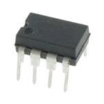
M TC962 High Current Charge Pump DC-to-DC Converter Features General Description • Pin Compatible With TC7662/ICL7662/SI7661 The TC962 is an advanced version of the industry (cid:127) High Output Current 80mA standard TC7662 high voltage DC-to-DC converter. Using improved design techniques and CMOS (cid:127) No External Diodes Required construction, the TC962 can source as much as 80mA (cid:127) Wide Operating Range 3V to 18V versus the 7662’s 20mA capability. (cid:127) Low Output Impedance 28 Ω Typ. As an inverter, the TC962 can put out voltages as high (cid:127) No Low Voltage Terminal Required as 18V and as low as 3V without the need for external (cid:127) Application Zener On-Chip diodes. The output impedance of the device is a low (cid:127) OSC Frequency Doubling Pin Option for Smaller 28Ω (with the proper capacitors), voltage conversion Output Capacitors efficiency is 99.9%, and power conversion efficiency is 97%. Applications The low voltage terminal (pin 6) required in some (cid:127) Laptop Computers TC7662 applications has been eliminated. Grounding (cid:127) Disk Drives this terminal will double the oscillator frequency from 12kHz to 24kHz. This will allow the use of smaller (cid:127) Process Instrumentation capacitors for the same output current and ripple, in (cid:127) µP-Based Controllers most applications. Only two external capacitors are required for inverter applications. In the event an Device Selection Table external clock is needed to drive the TC962 (such as paralleling), driving this pin directly will cause the Operating Part internal oscillator to sync to the external clock. Package Temp. Number Range Pin 1, which is used as a test pin on the 7662, is a voltage reference zener on the TC962. This zener TC962COE 16-Pin SOIC Wide 0°C to +70°C (6.4V at 5mA) has a dynamic impedance of 12Ω and is TC962CPA 8-Pin Plastic DIP 0°C to +70°C intended for use where the TC962 is supplying current TC962EPA 8-Pin Plastic DIP -40°C to +85°C to external regulator circuitry and a reference is needed for the regulator circuit. (See Section3.0 Applications TC962IJA 8-Pin CERDIP -25°C to +85°C Information). TC962MJA 8-Pin CERDIP -55°C to +125°C The TC962 is compatible with the LTC1044, SI7661 and ICL7662. It should be used in designs that require greater power and/or less input to output voltage drop. It offers superior performance over the ICL7660S. Package Type 16-Pin SOIC Wide Zener 8-Pin DIP Cathode 1 16 VDD 8-Pin CERDIP NC 2 15 NC CaZtheondeer 1 (cid:127) 8 VDD C+ 3 14 COSC C+ 2 TC962CPA 7 COSC NC 4 13 NC TC962EPA GND 5 TC962COE 12 FREQ x 2 GND 3 6 FREQ x 2 TC962IJA C– 4 TC962MJA 5 VOUT NC 6 11 NC C– 7 10 VOUT NC 8 9 NC 2002 Microchip Technology Inc. DS21484B-page 1
TC962 Functional Block Diagram 8 VDD FREQ x 2 6 I I TC962 OSC/C– 7 Timing Level P SW1 Shift Q + F/F 2 CAP+ C – Q Level N SW4 + Comparator Shift CP with Hysteresis External 3 GND 1 Zener Cathode VREF 6.4V + Level N SW2 OUT CR Shift EXT 4 – CAP RL Level N SW3 Shift 5 VOUT DS21484B-page 2 2002 Microchip Technology Inc.
TC962 1.0 ELECTRICAL *Stresses above those listed under "Absolute Maximum Ratings" may cause permanent damage to the device. These CHARACTERISTICS are stress ratings only and functional operation of the device at these or any other conditions above those indicated in the Absolute Maximum Ratings* operation sections of the specifications is not implied. Supply Voltage (V to GND)..............................+18V Exposure to Absolute Maximum Rating conditions for DD extended periods may affect device reliability. Input Voltage Any Pin .........................(V +0.3) to (V -0.3) (Note 1) DD SS Current Into Any Pin............................................10mA ESD Protection................................................±2000V Output Short Circuit...........Continuous (at 5.5V Input) Package Power Dissipation (T ≤ 70°C) A SOIC.......................................................760 mW PDIP........................................................730 mW CERDIP..................................................800 mW Package Thermal Resistance CERDIP, Rθ .........................................90°C/W J-A PDIP, Rθ ............................................140°C/W J-A Operating Temperature Range CPA, COE.......................................0°C to +70°C IJA................................................-25°C to +85°C EPA..............................................-40°C to +85°C MJA............................................-55°C to +125°C Storage Temperature Range .............-65°C to +150°C TC962 ELECTRICAL SPECIFICATIONS Electrical Characteristics: V = 15V, T = 25°C (See Figure3-1) unless otherwise noted. DD A Symbol Parameter Min Typ Max Units Test Conditions V Supply Voltage 3 — 18 V DD I Supply Current — — — µA R = ∞ S L V = 15V — 510 700 T = +25°C DD A — 560 — 0 ≤ T ≤ +70°C A — 650 — -55°C ≤ T ≤ +125°C A V = 5V — 190 — T = +25°C DD A — 210 — 0 ≤ T ≤ +70°C A — 210 — -55°C ≤ T ≤ +125°C A R Output Source — 32 37 Ω I = 20mA, V = 15V O L DD Resistance — 35 40 I = 80mA, V = 15V L DD — — 50 I = 3mA, V = 5V L DD F Oscillator Frequency — 12 — kHz Pin 6 Open OSC — 24 — Pin 6 GND P Power Efficiency 93 97 — % R = 2kΩ EFF L — — — V Voltage Efficiency 99 99.9 — % R = ∞ DEF L — — — Over temperature range 96 — — V Zener Voltage 6.0 6.2 6.4 V I = 5mA Z Z Z Zener Impedance — 12 — Ω I = 2.5mA to 7.5mA ZT L Note 1: Connecting any input terminal to voltages greater than V+ or less than GND may cause destructive latch-up. It is recommended that no inputs from sources operating from external supplies be applied prior to "power up" of the TC962. 2002 Microchip Technology Inc. DS21484B-page 3
TC962 2.0 PIN DESCRIPTIONS The descriptions of the pins are listed in Table 2-1. TABLE 2-1: PIN FUNCTION TABLE Pin No. (8-Pin DIP) Symbol Description (8-Pin CERDIP) 1 Zener Cathode Cathode of internal zener diode. 2 C+ Positive side of external CP capacitor (pump cap). 3 GND Ground terminal. 4 C- Negative side of external CP capacitor (pump cap). 5 V Output voltage. OUT 6 FREQ x 2 If grounded, frequency doubles. 7 C Capacitor to GND will decrease frequency. OSC 8 V Input voltage. DD Pin No. Symbol Description (16-Pin SOIC) 1 Zener Cathode Cathode of internal zener diode. 2 NC No connect. 3 C+ Positive side of external CP capacitor (pump cap). 4 NC No connect. 5 GND Ground terminal. 6 NC No connect. 7 C- Negative side of external CP capacitor (pump cap). 8 NC No connect. 9 NC No connect. 10 V Output voltage. OUT 11 NC No connect. 12 FREQ x 2 If grounded, frequency doubles. 13 NC No connect. 14 C Capacitor to GND will decrease frequency. OSC 15 NC No connect. 16 V Input voltage. DD DS21484B-page 4 2002 Microchip Technology Inc.
TC962 3.0 APPLICATIONS INFORMATION internal to the TC962. Grounding pin 6 will turn on a current source and double the frequency. This will 3.1 Theory of Operation double the charge current going into the internal capacitor, as well as any capacitor added to pin 7. The TC962 is a capacitive pump (sometimes called a A zener diode has been added to the TC962 for use as switched capacitor circuit), where four MOSFET a reference in building external regulators. This zener switches control the charge and discharge of a runs from pin 1 to ground. capacitor. The functional block diagram shows how the switching 3.2 Latch Up action works. SW1 and SW2 are turned on simulta- neously, charging C to the supply voltage, V . This All CMOS structures contain a parasitic SCR. Care P IN assumes that the on resistance of the MOSFETs in must be taken to prevent any input from going above or series with the capacitor results in a charging time below the supply rail, or latch up will occur. The result (3time constants) that is less than the on time provided of latch up is an effective short between VDD and VSS. by the oscillator frequency as shown: Unless the power supply input has a current limit, this latch up phenomena will result in damage to the device. 3 (R C ) < C /(0.5 f ) DS(ON) P P OSC (See AN763 Latch-up Protection of CMOS ICs.) In the next cycle, SW1 and SW2 are turned off and after a very short interval of all switches being off (this FIGURE 3-1: TEST CIRCUIT prevents large currents from occurring due to cross conduction), SW3 and SW4 are turned on. The charge 690 in C is then transferred to C , but with the polarity inverPted. In this way, a negativeR voltage is now derived. 1 8 IS V+ NC (+5V) An oscillator supplies pulses to a flip-flop that is then 2 7 IL fderdiv eto eaa cshe t soef t leovf esl wshiticftheerss . aTth oensee -lheavlef l thshei ftoesrcsi ltlahteonr CP + 10µF 3 TC962 COSC RL frequency. 4 5 VOUT (–5V) The oscillator has two pins that control the frequency of oscillation. Pin 7 can have a capacitor added that is CR + 10µF returned to ground. This will lower the frequency of the oscillator by adding capacitance to the timing capacitor FIGURE 3-2: TYPICAL APPLICATIONS Combined Negative Converter and Positive Multiplier Split V+ In Half V+ V+ 1 8 1 8 2 7 VD1 2 7 CP2 +10µF34 TC962 65 VOUT = –V+ VD2 + V2VO U+ T– 2=V D CP+ 10µF34 TC962 65 CR1 10µF 10µF V+ CP1+ + CR+ 10µF VOUT = 2 Lowering Output Resistance by Paralleling Devices Positive Voltage Multiplier V+ V+ 1 8 1 8 1 8 VD1 2 7 2 7 2 7 CP1+ 10µF34 TC962 65 CP2+ 10µF 34 TC962 65 34 TC962 65 CP+ 10µFVCDP2+ 10 µV2FVO +U –T2 =VD VOUT CR 10µF + 2002 Microchip Technology Inc. DS21484B-page 5
TC962 4.0 TYPICAL CHARACTERISTICS Note: The graphs and tables provided following this note are a statistical summary based on a limited number of samples and are provided for informational purposes only. The performance characteristics listed herein are not tested or guaranteed. In some graphs or tables, the data presented may be outside the specified operating range (e.g., outside specified power supply range) and therefore outside the warranted range. Circuit of Figure3-1, C = C = 10µF, C ≈ C ≈ 1Ω. P R PESR RESR Supply Current vs. Temperature Oscillator Frequency vs. COSC Frequency vs. Temperature 700 20 TA = +25°C COSC = FREQ x 2 = OPEN 600 10k 18 µSUPPLY CURRENT (A) 254300000000 V + V = + 1 =5 V15V FREQUENCY (Hz)110k0 FREQUENCY (kHz)11116420 100 8 0 10 6 -60 -40 -20 0 20 40 60 80100120 140 1 10 100 1000 10,000 -60 -40 -20 0 20 40 60 80100 120 140 TEMPERATURE (°C) CAPACITANCE (pF) TEMPERATURE (°C) Output Resistance vs. Temperature Current vs. Zener Voltage Power Conversion Efficiency vs. ILOAD ΩOUTPUT RESISTANCE ( ) 876543000000 V+ = 5V IL = 3mAV + = 15V IL = 20mA CURRENT (mA)54320000 TA = +25°C R CONVERSION EFFICIENCY (%)14530869700000000 EFFICIENCY TA = +25SC°UUCPRPRLEYNT 11119476305205505500SUPPLY CURRENT (mA) 20 10 WE 20 30 PO 10 15 10 0 0 0 -60 -40 -20 0 20 40 60 80100 120140 4.5 4.0 5.5 6.0 6.5 7.0 8 16 24 32 40 48 56 64 72 80 TEMPERATURE (°C) ZENER VOLTAGE (V) LOAD CURRENT (mA) Output Resistance vs. Input Voltage 110 100 TA = +25°C ΩCE ( ) 9800 N A 70 T ESIS 60 3mA 20mA R 50 T U 40 P UT 30 O 20 10 0 2 4 6 8 10 12 14 16 18 20 INPUT VOLTAGE (V) DS21484B-page 6 2002 Microchip Technology Inc.
TC962 5.0 PACKAGING INFORMATION 5.1 Package Marking Information Package marking data not available at this time. 5.2 Package Dimensions 8-Pin CDIP (Narrow) .110 (2.79) .090 (2.29) PIN1 .300 (7.62) .230 (5.84) .055 (1.40) MAX. .020 (0.51) MIN. .400 (10.16) .320 (8.13) .370 (9.40) .290 (7.37) .040 (1.02) .200 (5.08) .020 (0.51) .160 (4.06) ..210205 ((53..0188)) .150M (I3N..81) ..001058 ((00..3280)) 3°MIN. .400 (10.16) .320 (8.13) .065 (1.65) .020 (0.51) .045 (1.14) .016 (0.41) Dimensions: inches (mm) 8-Pin Plastic DIP PIN1 .260 (6.60) .240 (6.10) .045 (1.14) .070 (1.78) .030 (0.76) .040 (1.02) .310 (7.87) .400 (10.16) .290 (7.37) .348 (8.84) .200 (5.08) .140 (3.56) .040 (1.02) .020 (0.51) .015 (0.38) 3°MIN. .150 (3.81) .008 (0.20) .115 (2.92) .400 (10.16) .310 (7.87) .110 (2.79) .022 (0.56) .090 (2.29) .015 (0.38) Dimensions: inches (mm) 2002 Microchip Technology Inc. DS21484B-page 7
TC962 Package Dimensions (Continued) 16-Pin SOIC (Wide) PIN 1 .299 (7.59) .419 (10.65) .291 (7.40) .398 (10.10) .413 (10.49) .398 (10.10) .104 (2.64) .097 (2.46) 8° .013 (0.33) MAX. .009 (0.23) .012 (0.30) .050 (1.27) TYP. .019 (0.48) .004 (0.10) .050 (1.27) .014 (0.36) .016 (0.40) Dimensions: inches (mm) DS21484B-page 8 2002 Microchip Technology Inc.
TC962 Sales and Support Data Sheets Products supported by a preliminary Data Sheet may have an errata sheet describing minor operational differences and recom- mended workarounds. To determine if an errata sheet exists for a particular device, please contact one of the following: 1. Your local Microchip sales office 2. The Microchip Corporate Literature Center U.S. FAX: (480) 792-7277 3. The Microchip Worldwide Site (www.microchip.com) Please specify which device, revision of silicon and Data Sheet (include Literature #) you are using. New Customer Notification System Register on our web site (www.microchip.com/cn) to receive the most current information on our products. 2002 Microchip Technology Inc. DS21484B-page9
TC962 NOTES: DS21484B-page10 2002 Microchip Technology Inc.
TC962 Information contained in this publication regarding device Trademarks applications and the like is intended through suggestion only and may be superseded by updates. It is your responsibility to The Microchip name and logo, the Microchip logo, FilterLab, ensure that your application meets with your specifications. KEELOQ, microID, MPLAB, PIC, PICmicro, PICMASTER, No representation or warranty is given and no liability is PICSTART, PRO MATE, SEEVAL and The Embedded Control assumed by Microchip Technology Incorporated with respect Solutions Company are registered trademarks of Microchip Tech- to the accuracy or use of such information, or infringement of nology Incorporated in the U.S.A. and other countries. patents or other intellectual property rights arising from such dsPIC, ECONOMONITOR, FanSense, FlexROM, fuzzyLAB, use or otherwise. Use of Microchip’s products as critical com- In-Circuit Serial Programming, ICSP, ICEPIC, microPort, ponents in life support systems is not authorized except with Migratable Memory, MPASM, MPLIB, MPLINK, MPSIM, express written approval by Microchip. No licenses are con- MXDEV, PICC, PICDEM, PICDEM.net, rfPIC, Select Mode veyed, implicitly or otherwise, under any intellectual property and Total Endurance are trademarks of Microchip Technology rights. Incorporated in the U.S.A. Serialized Quick Turn Programming (SQTP) is a service mark of Microchip Technology Incorporated in the U.S.A. All other trademarks mentioned herein are property of their respective companies. © 2002, Microchip Technology Incorporated, Printed in the U.S.A., All Rights Reserved. Printed on recycled paper. Microchip received QS-9000 quality system certification for its worldwide headquarters, design and wafer fabrication facilities in Chandler and Tempe, Arizona in July 1999 and Mountain View, California in March 2002. The Company’s quality system processes and procedures are QS-9000 compliant for its PICmicro® 8-bit MCUs, KEELOQ® code hopping devices, Serial EEPROMs, microperipherals, non-volatile memory and analog products. In addition, Microchip’s quality system for the design and manufacture of development systems is ISO 9001 certified. 2002 Microchip Technology Inc. DS21484B-page 11
M WORLDWIDE SALES AND SERVICE AMERICAS ASIA/PACIFIC Japan Corporate Office Australia Microchip Technology Japan K.K. Benex S-1 6F 2355 West Chandler Blvd. Microchip Technology Australia Pty Ltd 3-18-20, Shinyokohama Chandler, AZ 85224-6199 Suite 22, 41 Rawson Street Kohoku-Ku, Yokohama-shi Tel: 480-792-7200 Fax: 480-792-7277 Epping 2121, NSW Kanagawa, 222-0033, Japan Technical Support: 480-792-7627 Australia Tel: 81-45-471- 6166 Fax: 81-45-471-6122 Web Address: http://www.microchip.com Tel: 61-2-9868-6733 Fax: 61-2-9868-6755 Rocky Mountain China - Beijing Korea 2355 West Chandler Blvd. Microchip Technology Consulting (Shanghai) Microchip Technology Korea Chandler, AZ 85224-6199 Co., Ltd., Beijing Liaison Office 168-1, Youngbo Bldg. 3 Floor Tel: 480-792-7966 Fax: 480-792-7456 Unit 915 Samsung-Dong, Kangnam-Ku Bei Hai Wan Tai Bldg. Seoul, Korea 135-882 Atlanta No. 6 Chaoyangmen Beidajie Tel: 82-2-554-7200 Fax: 82-2-558-5934 500 Sugar Mill Road, Suite 200B Beijing, 100027, No. China Singapore Atlanta, GA 30350 Tel: 86-10-85282100 Fax: 86-10-85282104 Microchip Technology Singapore Pte Ltd. Tel: 770-640-0034 Fax: 770-640-0307 China - Chengdu 200 Middle Road Boston #07-02 Prime Centre Microchip Technology Consulting (Shanghai) 2 Lan Drive, Suite 120 Singapore, 188980 Co., Ltd., Chengdu Liaison Office Westford, MA 01886 Tel: 65-6334-8870 Fax: 65-6334-8850 Rm. 2401, 24th Floor, Tel: 978-692-3848 Fax: 978-692-3821 Taiwan Ming Xing Financial Tower Chicago No. 88 TIDU Street Microchip Technology Taiwan 333 Pierce Road, Suite 180 Chengdu 610016, China 11F-3, No. 207 Itasca, IL 60143 Tel: 86-28-6766200 Fax: 86-28-6766599 Tung Hua North Road Tel: 630-285-0071 Fax: 630-285-0075 China - Fuzhou Taipei, 105, Taiwan Dallas Tel: 886-2-2717-7175 Fax: 886-2-2545-0139 Microchip Technology Consulting (Shanghai) 4570 Westgrove Drive, Suite 160 Co., Ltd., Fuzhou Liaison Office Addison, TX 75001 Unit 28F, World Trade Plaza EUROPE Tel: 972-818-7423 Fax: 972-818-2924 No. 71 Wusi Road Detroit Fuzhou 350001, China Denmark Tri-Atria Office Building Tel: 86-591-7503506 Fax: 86-591-7503521 Microchip Technology Nordic ApS 32255 Northwestern Highway, Suite 190 China - Shanghai Regus Business Centre Farmington Hills, MI 48334 Microchip Technology Consulting (Shanghai) Lautrup hoj 1-3 Tel: 248-538-2250 Fax: 248-538-2260 Co., Ltd. Ballerup DK-2750 Denmark Kokomo Room 701, Bldg. B Tel: 45 4420 9895 Fax: 45 4420 9910 2767 S. Albright Road Far East International Plaza France Kokomo, Indiana 46902 No. 317 Xian Xia Road Microchip Technology SARL Tel: 765-864-8360 Fax: 765-864-8387 Shanghai, 200051 Parc d’Activite du Moulin de Massy Los Angeles Tel: 86-21-6275-5700 Fax: 86-21-6275-5060 43 Rue du Saule Trapu 18201 Von Karman, Suite 1090 China - Shenzhen Batiment A - ler Etage Irvine, CA 92612 Microchip Technology Consulting (Shanghai) 91300 Massy, France Tel: 949-263-1888 Fax: 949-263-1338 Co., Ltd., Shenzhen Liaison Office Tel: 33-1-69-53-63-20 Fax: 33-1-69-30-90-79 New York Rm. 1315, 13/F, Shenzhen Kerry Centre, Germany 150 Motor Parkway, Suite 202 Renminnan Lu Microchip Technology GmbH Hauppauge, NY 11788 Shenzhen 518001, China Gustav-Heinemann Ring 125 Tel: 631-273-5305 Fax: 631-273-5335 Tel: 86-755-2350361 Fax: 86-755-2366086 D-81739 Munich, Germany San Jose Hong Kong Tel: 49-89-627-144 0 Fax: 49-89-627-144-44 Italy Microchip Technology Inc. Microchip Technology Hongkong Ltd. 2107 North First Street, Suite 590 Unit 901-6, Tower 2, Metroplaza Microchip Technology SRL San Jose, CA 95131 223 Hing Fong Road Centro Direzionale Colleoni Tel: 408-436-7950 Fax: 408-436-7955 Kwai Fong, N.T., Hong Kong Palazzo Taurus 1 V. Le Colleoni 1 Toronto Tel: 852-2401-1200 Fax: 852-2401-3431 20041 Agrate Brianza Milan, Italy 6285 Northam Drive, Suite 108 India Tel: 39-039-65791-1 Fax: 39-039-6899883 Mississauga, Ontario L4V 1X5, Canada Microchip Technology Inc. United Kingdom Tel: 905-673-0699 Fax: 905-673-6509 India Liaison Office Divyasree Chambers Arizona Microchip Technology Ltd. 505 Eskdale Road 1 Floor, Wing A (A3/A4) No. 11, O’Shaugnessey Road Winnersh Triangle Bangalore, 560 025, India Wokingham Tel: 91-80-2290061 Fax: 91-80-2290062 Berkshire, England RG41 5TU Tel: 44 118 921 5869 Fax: 44-118 921-5820 03/01/02 (cid:1)(cid:2)(cid:3)(cid:4)(cid:5)(cid:6)(cid:7)(cid:6)(cid:8)(cid:1) DS21484B-page 12 2002 Microchip Technology Inc.
Mouser Electronics Authorized Distributor Click to View Pricing, Inventory, Delivery & Lifecycle Information: M icrochip: TC962COE713 TC962COE TC962EPA TC962CPA