ICGOO在线商城 > 集成电路(IC) > PMIC - 稳压器 - DC DC 开关稳压器 > TPS55386PWP
 Datasheet下载
- 型号: TPS55386PWP
- 制造商: Texas Instruments
- 库位|库存: xxxx|xxxx
- 要求:
| 数量阶梯 | 香港交货 | 国内含税 |
| +xxxx | $xxxx | ¥xxxx |
查看当月历史价格
查看今年历史价格
TPS55386PWP产品简介:
ICGOO电子元器件商城为您提供TPS55386PWP由Texas Instruments设计生产,在icgoo商城现货销售,并且可以通过原厂、代理商等渠道进行代购。 TPS55386PWP价格参考¥13.52-¥25.24。Texas InstrumentsTPS55386PWP封装/规格:PMIC - 稳压器 - DC DC 开关稳压器, 可调式 降压 开关稳压器 IC 正 0.8V 2 输出 3A 16-TSSOP(0.173",4.40mm 宽)裸露焊盘。您可以下载TPS55386PWP参考资料、Datasheet数据手册功能说明书,资料中有TPS55386PWP 详细功能的应用电路图电压和使用方法及教程。
TPS55386PWP 是由 Texas Instruments(德州仪器)生产的一款 PMIC(电源管理集成电路),属于 DC-DC 开关稳压器类别。该型号的应用场景主要包括以下几个方面:

1. 便携式电子设备:TPS55386PWP 适合用于便携式设备,如智能手机、平板电脑和笔记本电脑等。其高效能转换能力和小尺寸设计使其成为这些设备的理想选择,能够为内部组件提供稳定的电源供应。

2. 通信设备:在无线通信基站、路由器和交换机等网络设备中,TPS55386PWP 可以为射频模块、处理器和其他关键组件提供高效的电源管理。其低功耗特性和高效率有助于减少热量产生,从而提高设备的整体性能。

3. 工业自动化:该芯片适用于工业控制和自动化系统,例如可编程逻辑控制器(PLC)、传感器接口和数据采集系统。它能够在苛刻的工业环境中提供可靠的电源解决方案,确保系统的稳定运行。

4. 消费类电子产品:包括数码相机、游戏机和个人媒体播放器等消费类产品。TPS55386PWP 的灵活性和高效性使得它可以满足这些产品对电源的不同需求,同时保持较小的电路板占用面积。

5. 医疗设备:在便携式医疗设备如血糖仪、脉搏血氧仪和便携式超声波设备中,TPS55386PWP 提供了精确而稳定的电源支持,这对于确保测量结果的准确性至关重要。

总之,TPS55386PWP 凭借其高效率、低静态电流和紧凑的设计,在需要高效电源管理和小型化解决方案的各种应用领域中表现出色。
| 参数 | 数值 |
| 产品目录 | 集成电路 (IC)半导体 |
| 描述 | IC REG BUCK ADJ 3A DL 16HTSSOP稳压器—开关式稳压器 3A Dual Non-Synch Buck Converter |
| 产品分类 | |
| 品牌 | Texas Instruments |
| 产品手册 | |
| 产品图片 |
|
| rohs | 符合RoHS无铅 / 符合限制有害物质指令(RoHS)规范要求 |
| 产品系列 | 电源管理 IC,稳压器—开关式稳压器,Texas Instruments TPS55386PWP- |
| 数据手册 | |
| 产品型号 | TPS55386PWP |
| PWM类型 | 电流模式 |
| 产品种类 | 稳压器—开关式稳压器 |
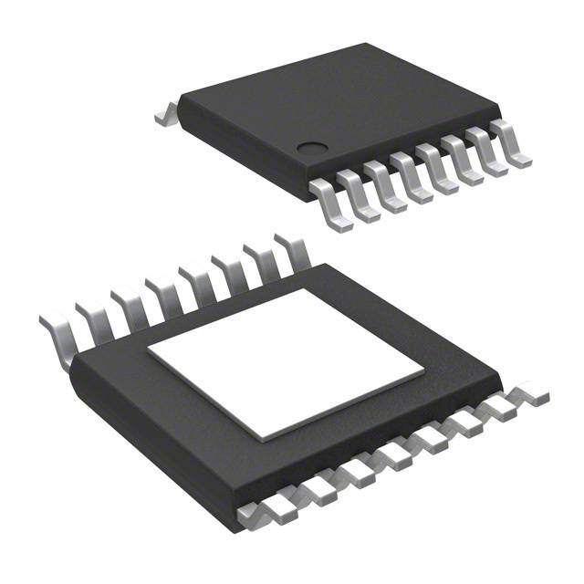
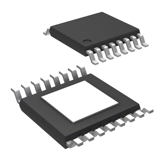
| 供应商器件封装 | 16-HTSSOP |
| 其它名称 | 296-34622-5 |
| 包装 | 管件 |
| 单位重量 | 62.700 mg |
| 同步整流器 | 无 |
| 商标 | Texas Instruments |
| 安装类型 | 表面贴装 |
| 安装风格 | SMD/SMT |
| 宽度 | 4.4 mm |
| 封装 | Tube |
| 封装/外壳 | 16-TSSOP (0.173", 4.40mm 宽)裸焊盘 |
| 封装/箱体 | HTSSOP-16 |
| 工作温度 | -40°C ~ 125°C |
| 工作温度范围 | - 40 C to + 125 C |
| 工厂包装数量 | 90 |
| 开关频率 | 600 kHz |
| 拓扑结构 | Buck |
| 最大工作温度 | + 125 C |
| 最大输入电压 | 28 V |
| 最小工作温度 | - 40 C |
| 最小输入电压 | 4.5 V |
| 标准包装 | 90 |
| 电压-输入 | 4.5 V ~ 28 V |
| 电压-输出 | 0.8 V ~ 25.2 V |
| 电流-输出 | 3A |
| 类型 | 降压(降压) |
| 系列 | TPS55386 |
| 设计资源 | http://www.digikey.com/product-highlights/cn/zh/texas-instruments-webench-design-center/3176 |
| 输入电压 | 4.5 V to 28 V |
| 输出数 | 2 |
| 输出电压 | 0.8 V to 25.2 V |
| 输出电流 | 3 A |
| 输出端数量 | 2 Output |
| 输出类型 | 可调式 |
| 配用 | /product-detail/zh/TPS55386EVM-363/296-31211-ND/2047973 |
| 频率-开关 | 630kHz |


- 商务部:美国ITC正式对集成电路等产品启动337调查
- 曝三星4nm工艺存在良率问题 高通将骁龙8 Gen1或转产台积电
- 太阳诱电将投资9.5亿元在常州建新厂生产MLCC 预计2023年完工
- 英特尔发布欧洲新工厂建设计划 深化IDM 2.0 战略
- 台积电先进制程称霸业界 有大客户加持明年业绩稳了
- 达到5530亿美元!SIA预计今年全球半导体销售额将创下新高
- 英特尔拟将自动驾驶子公司Mobileye上市 估值或超500亿美元
- 三星加码芯片和SET,合并消费电子和移动部门,撤换高东真等 CEO
- 三星电子宣布重大人事变动 还合并消费电子和移动部门
- 海关总署:前11个月进口集成电路产品价值2.52万亿元 增长14.8%


PDF Datasheet 数据手册内容提取
TPS55383,, TPS55386 www.ti.com......................................................................................................................................................................................... SLUS818–SEPTEMBER2008 3-A DUAL NON-SYNCHRONOUS CONVERTER WITH INTEGRATED HIGH-SIDE MOSFET AND EXTERNAL COMPENSATION FEATURES CONTENTS 1 • 4.5-Vto28-VInputRange DeviceRatings 2 23 • OutputVoltage0.8Vto90%ofInputVoltage ElectricalCharacteristics 4 • OutputCurrentUpto3A DeviceInformation 10 • TwoFixedSwitchingFrequencyVersions: ApplicationInformation 13 – TPS55383:300kHz DesignExamples 30 AdditionalReferences 39 – TPS55386:600kHz • ThreeSelectableLevelsofOvercurrent DESCRIPTION Protection(Output2) • 0.8-V1.75%VoltageReference The TPS55383 and TPS55386 are dual output, • 2.1-msInternalSoftStart non-synchronous buck converters capable of supporting3-Aoutputapplicationsthatoperatefroma • DualPWMOutputs180°Out-of-Phase 4.5-V to 28-V input supply voltage, and require output • RatiometricorSequentialStartupModes voltagesbetween0.8Vand90%oftheinputvoltage. • ConfigurableasDualOutputorTwo-Channel With an internally-determined operating frequency SingleOutputMultiphasefor6ampCapability and soft start time, these converters provide many • 85-mΩInternalHigh-SideMOSFETs featureswitha minimum of external components. The outputs of the two error amplifiers are accessible • CurrentModeControlwithExternal allowing user optimization of the feedback loop under Compensation a wide range of output filter characteristics. • Pulse-by-PulseOvercurrentProtection Channel1overcurrentprotection is set at 4.5 A, while • ThermalShutdownProtectionat+148°C Channel 2 overcurrent protection level is selected by connecting a pin to ground, to BP, or left floating. The • 16-PinPowerPAD™HTSSOPpackage setting levels are used to allow for scaling of external components for applications that do not need the full APPLICATIONS loadcapabilityofbothoutputs. • SetTopBox The outputs may be enabled independently, or • DigitalTV configured to allow either ratiometric or sequential • PowerforDSP startup sequencing. Additionally, the two outputs may • ConsumerElectronics bepoweredfromdifferentsources. V IN TPS55383 1 PVDD1 PVDD2 16 2 BOOT1 BOOT2 15 OUTPUT1 OUTPUT2 3 SW1 SW2 14 4 GND BP 13 5 EN1 SEQ 12 6 EN2 ILIM2 11 7 FB1 FB2 10 8 COMP1 COMP2 9 UDG-08045 1 Pleasebeawarethatanimportantnoticeconcerningavailability,standardwarranty,anduseincriticalapplicationsofTexas Instrumentssemiconductorproductsanddisclaimerstheretoappearsattheendofthisdatasheet. PowerPADisatrademarkofTexasInstruments. 2 Allothertrademarksarethepropertyoftheirrespectiveowners. 3 PRODUCTIONDATAinformationiscurrentasofpublicationdate. Copyright©2008,TexasInstrumentsIncorporated Products conform to specifications per the terms of the Texas Instruments standard warranty. Production processing does not necessarilyincludetestingofallparameters.
TPS55383,, TPS55386 SLUS818–SEPTEMBER2008......................................................................................................................................................................................... www.ti.com Thesedeviceshavelimitedbuilt-inESDprotection.Theleadsshouldbeshortedtogetherorthedeviceplacedinconductivefoam duringstorageorhandlingtopreventelectrostaticdamagetotheMOSgates. ORDERINGINFORMATION(1) DEVICENUMBER OPERATINGFREQUENCY(kHz) PACKAGE MEDIA UNITS(Pieces) TPS55383PWP Tube 90 300 TPS55383PWPR TapeandReel 2000 Plastic16-PinHTSSOP TPS55386PWP Tube 90 600 TPS55386PWPR TapeandReel 2000 (1) ForthemostcurrentpackageandorderinginformationseethePackageOptionAddendumattheendofthisdocument,orseetheTI websiteatwww.ti.com. DEVICE RATINGS ABSOLUTE MAXIMUM RATINGS(1) VALUE UNIT PVDD1,PVDD2,EN1,EN2 30 BOOT1,BOOT2 VSW+7 SW1,SW2 –2to30 SW1,SW2transient(<50ns) –3to31 Inputvoltagerange V BP 6.5 SEQ,ILIM2 –0.3to6.5 COMP1,COMP2 –0.3to3.5 FB1,FB2 –0.3to3 SW1,SW2outputcurrent 7 A BPloadcurrent 35 mA Tstg Storagetemperature –55to+165 TJ Operatingtemperature –40to+150 °C Solderingtemperature +260 (1) PermanentdevicedamagemayoccurifAbsoluteMaximumRatingsareexceeded.Functionaloperationshouldbelimitedtothe RecommendedDCOperatingConditionsdetailedinthisdatasheet.Exposuretoconditionsbeyondtheoperationallimitsforextended periodsoftimemayaffectdevicereliability. RECOMMENDED OPERATING CONDITIONS MIN MAX UNIT VPVDD2 Inputvoltage 4.5 28 V Operatingjunction TJ temperature –40 +125 °C 2 SubmitDocumentationFeedback Copyright©2008,TexasInstrumentsIncorporated ProductFolderLink(s):TPS55383TPS55386
TPS55383,, TPS55386 www.ti.com......................................................................................................................................................................................... SLUS818–SEPTEMBER2008 ELECTROSTATIC DISCHARGE (ESD) PROTECTION MIN UNIT Humanbodymodel 2k CDM 1.5k V MachineModel 250 PACKAGE DISSIPATION RATINGS(1)(2)(3) THERMALIMPEDANCE JUNCTION-TO-THERMAL TA=+25°C TA=+85°C PACKAGE PAD(°C/W) POWERRATING(W) POWERRATING(W) Plastic16-PinHTSSOP(PWP) 2.07(4) 1.6 1.0 (1) FormoreinformationonthePWPpackage,refertoTITechnicalBrief(SLMA002A). (2) TIdevicepackagesaremodeledandtestedforthermalperformanceusingprintedcircuitboarddesignsoutlinedinJEDECstandards JESD51-3andJESD51-7. (3) Forapplicationinformation,seethePowerDeratingsection. (4) T =+40°C/W. J-A Copyright©2008,TexasInstrumentsIncorporated SubmitDocumentationFeedback 3 ProductFolderLink(s):TPS55383TPS55386
TPS55383,, TPS55386 SLUS818–SEPTEMBER2008......................................................................................................................................................................................... www.ti.com ELECTRICAL CHARACTERISTICS –40°C≤T ≤+125°C,V =V =12V,unlessotherwisenoted. J PVDD1 PVDD2 PARAMETER TESTCONDITIONS MIN TYP MAX UNIT INPUTSUPPLY(PVDD) VPVDD1 Inputvoltagerange 4.5 28 V VPVDD2 IDDSDN Shutdown VEN1=VEN2=VPVDD2 70 150 m A IDDQ Quiescent,non-switching VFB=0.9V,OutputsOFF 1.8 3.0 SWnodeunloaded;MeasuredasBPsink mA IDDSW Quiescent,while-switching current 5 VUVLO Minimumturn-onvoltage PVDD2only 3.8 4.1 4.4 V VUVLO(hys) Hysteresis 400 600 mV tSTART(1)(2) Timefromstartuptosoftstartbegin CsiBmPu=lta1n0emoFus,lEyN1andEN2golow 2 ms ENABLE(EN) VEN1,VEN2 Enablethreshold 0.9 1.2 1.5 V Enablethresholdhysteresis(1) 50 mV IEN1.IEN2 Enablepull-upcurrent VEN1=VEN2=0V 6 12 m A tEN(1) Timefromenabletosoft-startbegin OtherENpin=GND 10 m s BPREGULATOR(BP) BP Regulatorvoltage 8V<PVDD2<28V 5 5.25 5.6 V BPLDO Dropoutvoltage PBVPDD2=4.5V;switching,noexternalloadon 400 550 mV IBP(1) Regulatorexternalload 2 mA IBPS Regulatorshortcircuit 4.5V<PVDD2<28V 10 20 30 OSCILLATOR TPS55383 255 310 375 fSW Switchingfrequency kHz TPS55386 510 630 750 tDEAD(1) Clockdeadtime 140 ns ERRORAMPLIFIER(EA)andVOLTAGEREFERENCE(REF) 0°C<TJ<+85°C 786 800 812 VFB1,VFB2 Feedbackinputvoltage mV –40°C<TJ<+125°C 784 812 IFB1,IFB2 Feedbackinputbiascurrent 3 50 nA gM1,gM2(1) ErrorAmplifiertransconductance 220 315 420 m S fp1,fp2(1) ErrorAmplifierdominantpolefrequency 5 6 kHz IISSIINNKK((CCOOMMPP12)), ErrorAmplifiersinkcurrentcapability VFB1=VFB2=0.9V,VCOMP=2V 15 30 40 m A IISSRRCC((CCOOMMPP12)), ErrorAmplifiersourcecurrentcapability VFB1=VFB2=0.7V,VCOMP=0V 15 30 40 m A SOFTSTART(SS) TSS1,TSS2 Softstarttime 1.5 2.1 2.7 ms (1) Ensuredbydesign.Notproductiontested. (2) Whenbothoutputsarestartedsimultaneously,a20-mAcurrentsourcechargestheBPcapacitor.Fastertimesarepossiblewithalower BPcapacitorvalue.MoreinformationcanbefoundintheInputUVLOandStartupsection. 4 SubmitDocumentationFeedback Copyright©2008,TexasInstrumentsIncorporated ProductFolderLink(s):TPS55383TPS55386
TPS55383,, TPS55386 www.ti.com......................................................................................................................................................................................... SLUS818–SEPTEMBER2008 ELECTRICAL CHARACTERISTICS (continued) –40°C≤T ≤+125°C,V =V =12V,unlessotherwisenoted. J PVDD1 PVDD2 PARAMETER TESTCONDITIONS MIN TYP MAX UNIT OVERCURRENTPROTECTION ICL1 CurrentlimitChannel1 3.6 4.5 5.6 VILIM2=VBP 3.6 4.5 5.6 A ICL2 CurrentlimitChannel2 VILIM2=(floating) 2.4 3.0 3.6 VILIM2=GND 1.15 1.50 1.75 VUV1 Low-leveloutputthresholdtodeclareafault Measuredatfeedbackpin. 670 730 mV VUV2 THICCUP(3) Hiccuptimeout 10 ms tON1(oc)(3) Minimumovercurrentpulsewidth 90 150 ns tON2(oc)(3) BOOTSTRAP RBOOT1, Bootstrapswitchresistance FromBPtoBOOT1orBPtoBOOT2, 18 Ω RBOOT2 IEXT=50mA OUTPUTSTAGE(Channel1andChannel2) RDS(on)(3) MOSFETonresistanceplusbondwireresistance TJ=+25°C,VPVDD2=8V 85 mΩ –40°C<TJ<+125°C,VPVDD2=8V 85 165 tON(min)(3) Minimumcontrollablepulsewidth ISWxpeakcurrent>1A(4) 100 200 ns DMIN MinimumDutyCycle VFB=0.9V 0 % TPS55383 fSW=300kHz 90 95 % DMAX MaximumDutyCycle TPS55386 fSW=600kHz 85 90 % ISW Switchingnodeleakagecurrent(sourcing) OutputsOFF 2 12 m A THERMALSHUTDOWN TSD(3) Shutdowntemperature 148 °C TSD(hys)(3) Hysteresis 20 (3) Ensuredbydesign.Notproductiontested. (4) SeeFigure14forI peakcurrent<1A. SWx Copyright©2008,TexasInstrumentsIncorporated SubmitDocumentationFeedback 5 ProductFolderLink(s):TPS55383TPS55386
TPS55383,, TPS55386 SLUS818–SEPTEMBER2008......................................................................................................................................................................................... www.ti.com TYPICAL CHARACTERISTICS QUIESCENTCURRENT(NON-SWITCHING) SHUTDOWNCURRENT vs vs JUNCTIONTEMPERATURE JUNCTIONTEMPERATURE 2.1 140 V =5.25 V V =28 V BP PVDDx 120 2.0 V =12 V PVDDx A m A m 100 -nt 1.9 -nt e e urr urr 80 C C nt 1.8 n e w sc do 60 Quie 1.7 Shut - - 40 DDQ ISD I 1.6 VPVDDx=4.5 V 20 1.5 0 -50 -25 0 25 50 75 100 125 -50 -25 0 25 50 75 100 125 T -Junction Temperature-°C T -Junction Temperature-°C J J Figure1. Figure2. UNDERVOLTAGELOCKOUTTHRESHOLD ENABLETHRESHOLDS vs vs JUNCTIONTEMPERATURE JUNCTIONTEMPERATURE 4.2 1.25 EN(Off) 4.1 V V 1.23 -ut UVLO(On) -ge o a ck 4.0 olt o V voltage L 3.9 hreshold 1.21 der UVLO(Off) e T 1.19 EN(On) Un 3.8 abl - n E O L - V U N1.17 V 3.7 VE 3.6 1.15 -50 -25 0 25 50 75 100 125 -50 -25 0 25 50 75 100 125 T -Junction Temperature-°C T -Junction Temperature-°C J J Figure3. Figure4. 6 SubmitDocumentationFeedback Copyright©2008,TexasInstrumentsIncorporated ProductFolderLink(s):TPS55383TPS55386
TPS55383,, TPS55386 www.ti.com......................................................................................................................................................................................... SLUS818–SEPTEMBER2008 TYPICAL CHARACTERISTICS (continued) SOFTSTARTTIME SWITCHINGFREQUENCY(300kHz) vs vs JUNCTIONTEMPERATURE JUNCTIONTEMPERATURE 3.5 350 V =5.25 V BP V =5.25 V BP s 3.0 Hz 330 m k - - y e c m n Ti ue oft Start 2.5 WM Freq 310 S P - - tSS 2.0 WM 290 P f 1.5 270 -50 -25 0 25 50 75 100 125 -50 -25 0 25 50 75 100 125 T -Junction Temperature-°C T -Junction Temperature-°C J J Figure5. Figure6. SWITCHINGFREQUENCY(600kHz) FEEDBACKBIASCURRENT vs vs JUNCTIONTEMPERATURE JUNCTIONTEMPERATURE 680 5 V =5.25 V BP 660 A 3 z n H - -k nt ncy 640 urre 1 e C M Frequ ck Bias W 620 a -1 b P d - e e M F W P - f 600 FB -3 I 580 -5 -50 -25 0 25 50 75 100 125 -50 -25 0 25 50 75 100 125 T -Junction Temperature-°C T -Junction Temperature-°C J J Figure7. Figure8. Copyright©2008,TexasInstrumentsIncorporated SubmitDocumentationFeedback 7 ProductFolderLink(s):TPS55383TPS55386
TPS55383,, TPS55386 SLUS818–SEPTEMBER2008......................................................................................................................................................................................... www.ti.com TYPICAL CHARACTERISTICS (continued) FEEDBACKVOLTAGE OVERCURRENTLIMIT(CH1,CH2HIGHLEVEL) vs vs JUNCTIONTEMPERATURE JUNCTIONTEMPERATURE 808 4.8 V =24 V PVDD V 803 4.6 m A - - ge mit Volta nt Li V =12 V k 798 re 4.4 PVDD dbac ercur e v e O -VFFB 793 -ICL 4.2 VPVDD=5 V 788 4.0 -50 -25 0 25 50 75 100 125 -50 -25 0 25 50 75 100 125 T -Junction Temperature-°C T -Junction Temperature-°C J J Figure9. Figure10. OVERCURRENTLIMIT(CH2MIDLEVEL) OVERCURRENTLIMIT(CH2LOWLEVEL) vs vs JUNCTIONTEMPERATURE JUNCTIONTEMPERATURE 3.4 1.8 VPVDDx=24 V V =24 V PVDDx 3.2 A A - - 1.6 mit mit Li Li nt nt e 3.0 e r r r r u u c c r r e e v v O O 1.4 - - L L C 2.8 C I I V =12 V PVDDx V =12 V PVDDx V =5 V PVDDx V =5 V PVDDx 2.6 1.2 -50 -25 0 25 50 75 100 125 -50 -25 0 25 50 75 100 125 T -Junction Temperature-°C T -Junction Temperature-°C J J Figure11. Figure12. 8 SubmitDocumentationFeedback Copyright©2008,TexasInstrumentsIncorporated ProductFolderLink(s):TPS55383TPS55386
TPS55383,, TPS55386 www.ti.com......................................................................................................................................................................................... SLUS818–SEPTEMBER2008 TYPICAL CHARACTERISTICS (continued) SWITCHINGNODELEAKAGECURRENT MINUMUMCONTROLLABLEPULSEWIDTH vs vs JUNCTIONTEMPERATURE LOADCURRENT 5 400 T (°C) A A m ns –40 nt- h- 350 T =–40°C 0 Curre 4 Widt 300 A 2855 e e s kag Pul Lea ble 250 a de 3 oll T =0°C No ntr 200 A g o n C hi m witc 2 mu 150 S ni - Mi W(off) -ON100 TA=25°C S t T =85°C I A 1 50 -50 -25 0 25 50 75 100 125 0 0.2 0.4 0.6 0.8 1.0 1.2 1.4 I -LoadCurrent-A T -JunctionTemperature-°C L J Figure13. Figure14. OVERCURRENTLIMIT vs SUPPLYVOLTAGE 5.0 4.5 4.0 A - OCL=3.0A OCL=4.5A mit 3.5 Li nt re 3.0 r u c r e v 2.5 O - OC 2.0 OCL=1.5A I 1.5 1.0 4 8 12 16 20 24 28 V -SupplyVoltage-V DD Figure15. Copyright©2008,TexasInstrumentsIncorporated SubmitDocumentationFeedback 9 ProductFolderLink(s):TPS55383TPS55386
TPS55383,, TPS55386 SLUS818–SEPTEMBER2008......................................................................................................................................................................................... www.ti.com DEVICE INFORMATION PIN CONNECTIONS HTSSOP(PWP) (TopView) PVDD1 1 16 PVDD2 BOOT1 2 15 BOOT2 SW1 3 14 SW2 GND 4 13 BP ThermalPad EN1 5 (bottomside) 12 SEQ EN2 6 11 ILIM2 FB1 7 10 FB2 COMP1 8 9 COMP2 TERMINALFUNCTIONS TERMINAL I/O DESCRIPTION NAME NO. InputsupplytothehighsidegatedriverforOutput1.Connecta22-nFto82-nFcapacitorfromthispin toSW1.ThiscapacitorischargedfromtheBPpinvoltagethroughaninternalswitch.Theswitchis BOOT1 2 I turnedONduringtheOFFtimeoftheconverter.ToslowdowntheturnONoftheinternalFET,asmall resistor(1Ωto3Ω)maybeplacedinserieswiththebootstrapcapacitor. InputsupplytothehighsidegatedriverforOutput2.Connecta22-nFto82-nFcapacitorfromthispin toSW2.ThiscapacitorischargedfromtheBPpinvoltagethroughaninternalswitch.Theswitchis BOOT2 15 I turnedONduringtheOFFtimeoftheconverter.ToslowdowntheturnONoftheinternalFET,asmall resistor(1Ωto3Ω)maybeplacedinserieswiththebootstrapcapacitor. Regulatedvoltagetochargethebootstrapcapacitors.BypassthispintoGNDwithalowESR(4.7-m F BP 13 - to10-m FX7RorX5R)ceramiccapacitor. OutputofErrorAmplifierforOutput1.AseriesconnectedR-CnetworkfromthispintoGNDservesto COMP1 8 O compensatethefeedbackloop.SeeFeedbackLoopCompensationComponentSelectionforfurther information. OutputofErrorAmplifierforOutput2.AseriesconnectedR-CnetworkfromthispintoGNDservesto COMP2 9 O compensatethefeedbackloop.SeeFeedbackLoopCompensationComponentSelectionforfurther information. ActivelowenableinputforOutput1.Ifthevoltageonthispinisgreaterthan1.55V,Output1is disabled(high-sideswitchisOFF).Avoltageoflessthan0.9VenablesOutput1andallowssoftstartof EN1 5 I Output1tobegin.AninternalcurrentsourcedrivesthispintoPVDD2ifleftfloating.Connectthispinto GNDfor"alwaysON"operation. ActivelowenableinputforOutput2.Ifthevoltageonthispinisgreaterthan1.55V,Output2is disabled(high-sideswitchisOFF).Avoltageoflessthan0.9VenablesOutput2andallowssoftstartof EN2 6 I Output2tobegin.AninternalcurrentsourcedrivesthispintoPVDD2ifleftfloating.Connectthispinto GNDfor"alwaysON"operation. VoltagefeedbackpinforOutput1.TheinternaltransconductanceerroramplifieradjuststhePWMfor Output1toregulatethevoltageatthispintotheinternal0.8-Vreference.Aseriesresistordividerfrom FB1 7 I Output1toground,withthecenterconnectiontiedtothispin,determinesthevalueoftheregulated outputvoltage.Compensationforthefeedbackloopisprovidedexternallytothedevice.SeeFeedback LoopCompensationComponentSelectionsectionforfurtherinformation. VoltagefeedbackpinforOutput2.TheinternaltransconductanceerroramplifieradjuststhePWMfor Output2toregulatethevoltageatthispintotheinternal0.8-Vreference.Aseriesresistordividerfrom FB2 10 I Output2toground,withthecenterconnectiontiedtothispin,determinesthevalueoftheregulated Outputvoltage.Compensationforthefeedbackloopisprovidedexternallytothedevice.SeeFeedback LoopCompensationComponentSelectionsectionforfurtherinformation. GND 4 - Groundpinforthedevice.ConnectdirectlytoThermalPad. CurrentlimitadjustpinforOutput2only.Thisfunctionisintendedtoallowauserwithasymmetrical loadcurrents(Output1loadcurrentmuchgreaterthanOutput2loadcurrent)tooptimizecomponent ILIM2 11 I scalingofthelowercurrentoutputwhilemaintainingpropercomponentderatinginaovercurrentfault condition.ThediscretelevelsareavailableasshowninTable2,CurrentLimitThresholdAdjustmentfor Output2.Note:Aninternal2-resistordivider(150-kΩeach)connectsBPtoILIM2andtoGND. 10 SubmitDocumentationFeedback Copyright©2008,TexasInstrumentsIncorporated ProductFolderLink(s):TPS55383TPS55386
TPS55383,, TPS55386 www.ti.com......................................................................................................................................................................................... SLUS818–SEPTEMBER2008 TERMINALFUNCTIONS(continued) TERMINAL I/O DESCRIPTION NAME NO. PowerinputtotheOutput1highsideMOSFETonly.ThispinshouldbelocallybypassedtoGNDwitha PVDD1 1 I lowESRceramiccapacitorof10-m Forgreater. ThePVDD2pinprovidespowertothedevicecontrolcircuitry,providesthepull-upfortheEN1andEN2 pinsandprovidespowertotheOutput2high-sideMOSFET.Thispinshouldbelocallybypassedto PVDD2 16 I GNDwithalowESRceramiccapacitorof10-m Forgreater.TheUVLOfunctionmonitorsPVDD2and enablesthedevicewhenPVDD2isgreaterthan4.1V. Thispinconfigurestheoutputstartupmode.IftheSEQpinisconnectedtoBP,thenwhenOutput2is enabled,Output1isallowedtostartafterOutput2hasreachedregulation;thatis,sequentialstartup whereOutput1isslavetoOutput2.IfEN2isallowedtogohighaftertheoutputshavebeenoperating, thenbothoutputsaredisabledimmediately,andtheoutputvoltagesdecayaccordingtotheloadthatis present.Forthissequenceconfiguration,tieEN1toground. IftheSEQpinisconnectedtoGND,thenwhenOutput1isenabled,Output2isallowedtostartafter Output1hasreachedregulation;thatis,sequentialstartupwhereOutput2isslavetoOutput1.IfEN1 isallowedtogohighaftertheoutputshavebeenoperating,thenbothoutputsaredisabledimmediately, SEQ 12 I andtheoutputvoltagesdecayaccordingtotheloadthatispresent.Forthissequenceconfiguration,tie EN2toground. Ifleftfloating,Output1andOutput2startratio-metricallywhenbothoutputsareenabledatthesame time.Theywillsoftstartataratedeterminedbytheirfinaloutputvoltageandenterregulationatthe sametime.IftheEN1andEN2pinsareallowedtooperateindependently,thenthetwooutputsalso operateindependently NOTE:Aninternaltworesistor(150-kΩeach)dividerconnectsBPtoSEQandtoGND.Seethe SequenceStatestable. Source(switching)outputforOutput1PWM.Asnubberisrecommendedtoreduceringingonthis SW1 3 O node.SeeSWNodeRingingforfurtherinformation. Source(switching)outputforOutput2PWM.Asnubberisrecommendedtoreduceringingonthis SW2 14 O node.SeeSWNodeRingingforfurtherinformation. ThermalPad - - ThispadmustbetiedexternallytoagroundplaneandtheGNDpin. Copyright©2008,TexasInstrumentsIncorporated SubmitDocumentationFeedback 11 ProductFolderLink(s):TPS55383TPS55386
TPS55383,, TPS55386 SLUS818–SEPTEMBER2008......................................................................................................................................................................................... www.ti.com BLOCK DIAGRAM 2 BOOT1 BP CLK1 Level 1 PVDD1 Shift Current f(I )+DC(ofst) Comparator DRAIN1 S Q + COMP1 8 R R Q + f(I ) FB1 10 DRAIN1 OvercurrentComp 0.8V + 3 SW1 REF f(ISLOPE1) f(IMAX1) BP SoftStart Weak SD1 1 CLK1 Anti-Cross Pull-Down Conduction MOSFET VDD2 f(I ) SLOPE1 Ramp Gen1 TSD 1.2MHz Divide CLK1 6mA 6mA Oscilator by2/4 f(I ) SLOPE2 EN1 5 SD1 Ramp Gen2 Internal SD2 EN2 6 Control CLK2 UVLO 150kW SEQ 12 BP FB1 Output Undervoltage 150kW 15 BOOT2 FB2 Detect BP CLK2 Level 16 PVDD2 Shift Current GND 4 Comparator FET f(I )+DC(ofst) DRAIN2 S Q Switch + COMP2 9 R R Q + f(I ) FB2 8 DRAIN2 OvercurrentComp 0.8V + 14 SW2 REF f(ISLOPE2) f(IMAX2) BP SoftStart Weak SD2 2 CLK2 Anti-Cross Pull-Down Conduction MOSFET 5.25-V BP 13 PVDD2 Regulator 150kW BP Level ILIM2 11 Select 150kW 0.8V REF References I (Settooneofthreelimits) MAX2 UDG-08044 12 SubmitDocumentationFeedback Copyright©2008,TexasInstrumentsIncorporated ProductFolderLink(s):TPS55383TPS55386
TPS55383,, TPS55386 www.ti.com......................................................................................................................................................................................... SLUS818–SEPTEMBER2008 APPLICATION INFORMATION FUNCTIONAL DESCRIPTION The TPS55383 and TPS55386 are dual output, non-synchronous converters. Each PWM channel contains an externally-compensated error amplifier, current mode pulse width modulator (PWM), switch MOSFET, enable, and fault protection circuitry. Common to the two channels are the internal voltage regulator, voltage reference, clockoscillator,andoutputvoltagesequencingfunctions. NOTE: Unless otherwise noted, the term TPS5538x applies to both the TPS55383 and TPS55386.Also,unlessotherwisenoted,alabel with a lowercase x appended implies thetermapplies to both outputs of the two modulator channels. For example, the term ENx implies both EN1 and EN2. Unless otherwise noted, all parametric values given are typical. Refer to the Electrical Characteristics for minimum and maximum values. Calculationsshouldbeperformedwithtolerancevaluestakenintoconsideration. VoltageReference Thebandgapcellcommontobothoutputsistrimmedto800mV. Oscillator The oscillator frequency is internally fixed at two times the SWx node switching frequency. The two outputs are internallyconfiguredtooperateonalternatingswitchcycles(thatis,180°out-of-phase). InputUndervoltageLockout(UVLO)andStartup When the voltage at the PVDD2 pin is less than 4.1 V, a portion of the internal bias circuitry is operational, and all other functions are held OFF. All of the internal MOSFETs are also held OFF. When the PVDD2 voltage rises above the UVLO turn-on threshold, the state of the enable pins determines the remainder of the internal startup sequence. If either output is enabled (ENx pulled low), the BP regulator turns on, charging the BP capacitor with a 20-mA current. When the BP pin is greater than 4 V, PWM is enabled and soft start begins, depending on the SEQmodeofoperationandtheEN1andEN2settings. Note that the internal regulator and control circuitry are powered from PVDD2. The voltage on PVDD1 may be higherorlowerthanPVDD2.(SeetheDualSupplyOperationsection.) EnableandTimedTurnOnoftheOutputs Each output has a dedicated (active low) enable pin. If left floating, an internal current source pulls the pin to PVDD2. By grounding, or by pulling the ENx pin to below approximately 1.2 V with an external circuit, the associatedoutputisenabledandsoftstartisinitiated. If both enable pins are left in the high state, the device operates in a shutdown mode, where the BP regulator is shut down and minimal functions are active. The total standby current from both PVDD pins is approximately 70 m Aat12-Vinputsupply. An R-C connected to an ENx pin may be used to delay the turn-on of the associated output after power is applied to PVDDx (see Figure 16). After power is applied to PVDD2, the voltage on the ENx pin slowly decays towards ground. Once the voltage decays to approximately 1.2 V, then the output is enabled and the startup sequence begins. If it is desired to enable the outputs of the device immediately upon the application of power to PVDD2,thenomitthesetwocomponentsandtietheENxpintoGNDdirectly. If an R-C circuit is used to delay the turn-on of the output, the resistor value must be much less than 1.2 V / 6 m A or 200 kΩ. A suggested value is 51 kΩ. This resistor value allows the ENx voltage to decay below the 1.2-V thresholdwhilethe6-m Abiascurrentflows. Thecapacitorvaluerequiredtodelaythestartuptime(aftertheapplicationofPVDD2)isshowninEquation1. Copyright©2008,TexasInstrumentsIncorporated SubmitDocumentationFeedback 13 ProductFolderLink(s):TPS55383TPS55386
TPS55383,, TPS55386 SLUS818–SEPTEMBER2008......................................................................................................................................................................................... www.ti.com t C= DELAY farads æV -2´I ´Rö R´lnç IN ENx ÷ è VTH-IENx´R ø (1) where: • RandCarethetimingcomponents • V isthe1.2-Venablethresholdvoltage TH • I isthe6m Aenablepinbiasingcurrent ENx Additional enable pin functionality is dictated by the state of the SEQ pin. (See the Output Voltage Sequencing section.) VDD2 5mA C ENx PVDDx VDDx + 1.2-V Threshold 1.25V R TPS5538x ENx V OUTx 0 t t + t DELAY DELAY SS T-Time Figure16.StartupDelaySchematic Figure17.StartupDelaywithR-ConEnable DESIGNHINT If delayed output voltage startup is not necessary, simply connect EN1 and EN2 to GND. This configuration allows the outputs to start immediately on valid application of PVDD2. If ENx is allowed to go high after the Outputx has been in regulation, the upper MOSFET shuts off, and the outputdecaysataratedeterminedbytheoutputcapacitorandtheload. The internal pulldown MOSFET remains intheOFFstate.(SeetheBootstrapforN-ChannelMOSFETsection.) OutputVoltageSequencing The TPS5538x allows single-pin programming of output voltage startup sequencing. During power-on, the state of the SEQ pin is detected. Based on whether the pin is tied to BP, to GND, or left floating, the outputs function asdescribedinTable1. 14 SubmitDocumentationFeedback Copyright©2008,TexasInstrumentsIncorporated ProductFolderLink(s):TPS55383TPS55386
TPS55383,, TPS55386 www.ti.com......................................................................................................................................................................................... SLUS818–SEPTEMBER2008 Table1.SequenceStates SEQPINSTATE MODE EN1 EN2 Ignoredbythedevice.whenV < EN2 enablethresholdvoltage TieEN1to<enablethresholdvoltage forBPtobeactivewhenV > BP Sequential,Output2thenOutput1 EN2 Active enablethresholdvoltage TieEN1to>enablethresholdvoltage forlowquiescentcurrent(BPinactive) whenV >enablethresholdvoltage EN2 Ignoredbythedevice.whenV < EN1 enablethresholdvoltage TieEN2to<enablethresholdvoltage forBPtobeactivewhenV > GND Sequential,Output1thenOutput2 Active EN1 enablethresholdvoltage TieEN2to>enablethresholdvoltage forlowquiescentcurrent(BPinactive) whenV >enablethresholdvoltage EN1 IndependentorRatiometric,Output1 Active.EN1andEN2mustbetied Active.EN1andEN2mustbetied (floating) andOutput2 togetherforRatio-metricstartup. togetherforRatio-metricstartup. IftheSEQpinisconnectedtoBP,then when Output 2 is enabled, Output 1 is allowed to start approximately 400 m safterOutput2hasreachedregulation;thatis,sequentialstartupwhereOutput1isslaveto Output 2. If EN2 is allowed to go high after the outputs have been operating, then both outputs are disabled immediately, and the outputvoltagesdecayaccordingtotheloadthatispresent. If the SEQ pin is connected to GND, then when Output 1 is enabled, Output 2 is allowed to start approximately 400 m s after Output 1 has reached regulation; that is, sequential startup where Output 2 is slave to Output 1. If EN1 is allowed to go high after the outputs have been operating, then both outputs are disabled immediately, andtheoutputvoltagesdecayaccordingtotheloadthatispresent. SEQ=BP SEQ=GND Sequential Sequential CH2thenCH1 CH1thenCH2 5-VVOUT1 (2V/div) 5-VVOUT1 (2V/div) 3.3-VVOUT2 (2V/div) 3.3-VVOUT2 (2V/div) T-Time-1ms/div T-Time-1ms/div Figure18.SEQPinTIedtoBP Figure19.SEQPinTiedtoGND NOTE: An R-C network connected to the ENx pin may be used in addition to the SEQ pin in sequential mode to delay the startup of the first output voltage. This approach may be necessary in systems with a large number of output voltages and elaborate voltage sequencingrequirements.SeeEnableandTimedTurnOnoftheOutputs. Copyright©2008,TexasInstrumentsIncorporated SubmitDocumentationFeedback 15 ProductFolderLink(s):TPS55383TPS55386
TPS55383,, TPS55386 SLUS818–SEPTEMBER2008......................................................................................................................................................................................... www.ti.com If the SEQ pin is left floating, Output 1 and Output 2 each start ratiometrically when both outputs are enabled at the same time. Output 1 and Output 2 soft start at a rate that is determined by the respective final output voltages and enter regulation at the same time. If the EN1 and EN2 pins are allowed to operate independently, thenthetwooutputsalsooperateindependently. 5-VVOUT1 (2V/div) 3.3-VVOUT2 (2V/div) T-Time-1ms/div Figure20.SEQPinFloating SoftStart Each output has a dedicated soft-start circuit. The soft-start voltage is an internal digital reference ramp to one of two noninverting inputs of the error amplifier. The other input is the (internal) precision 0.8-V reference. The total ramp time for the FB voltage to charge from 0 V to 0.8 V is about 2.1 ms. During a soft-start interval, the TPS5538x output slowly increases the voltage to the noninverting input of the error amplifier. In this way, the output voltage ramps up slowly until the voltage on the noninverting input to the error amplifier reaches the internal 0.8-V reference voltage. At that time, the voltage at the noninverting input to the error amplifier remains atthereferencevoltage. During the soft-start interval, pulse-by-pulse current limiting is in effect. If an overcurrent pulse is detected, six PWM pulses are skipped to allow the inductor current to decay before another PWM pulse is applied. (See the OutputOverloadProtectionsection.)Thereisnopulseskippingifacurrentlimitpulseisnotdetected. DESIGNHINT If the rate of rise of the input voltage (PVDDx) is such that the input voltage is too low to support the desired regulation voltage by the time soft-start has completed, then the output UV circuit may trip and cause a hiccup in the output voltage. In this case, use a timed delay startup from the ENx pin to delay the startup of the output until the PVDDx voltage has the capability of supporting the desired regulation voltage. See Operating Near Maximum Duty Cycle and Maximum Output Capacitance for related information. 16 SubmitDocumentationFeedback Copyright©2008,TexasInstrumentsIncorporated ProductFolderLink(s):TPS55383TPS55386
TPS55383,, TPS55386 www.ti.com......................................................................................................................................................................................... SLUS818–SEPTEMBER2008 OutputVoltageRegulation Each output has a dedicated feedback loop comprised of a voltage setting divider, an error amplifier, a pulse width modulator, and a switching MOSFET. The regulation output voltage is determined by a resistor divider connecting the output node, the FBx pin, and GND (see Figure 21). Assuming the value of the upper voltage setting divider is known, the value of the lower divider resistor for a desired output voltage is calculated by Equation2. V REF R2 = R1´ V -V OUT REF (2) where • V istheinternal0.8-Vreferencevoltage REF TPS5538x 1 PVDD1 PVDD2 16 2 BOOT1 BOOT2 15 OUTPUT1 3 SW1 SW2 14 4 GND BP 13 R1 5 EN1 SEQ 12 6 EN2 ILIM2 11 7 FB1 FB2 10 R2 8 COMP1 COMP2 9 UDG-08041 Figure21.VoltageSettingDividerNetworkforChannel1 DESIGNHINT There is a leakage current of up to 12 m A out of the SW pin when a single output of the TPS5538x is disabled. Keeping the series impedance of R1 + R2 less than 50 kΩ preventstheoutputfromfloatingabovethereferecevoltagewhilethecontrolleroutput isintheOFFstate. FeedbackLoopCompensationComponentSelection In the feedback signal path, the output voltage setting divider is followed by an internal g -type error amplifier M with a typical transconductance of 315 m S. An external series connected R-C circuit from the g amplifier output M (COMPxpin)togroundservesasthe compensation network for the converter. The signal from the error amplifier output is then buffered and combined with a slope compensation signal before it is mirrored to be referenced to the SW node. Here, it is compared with the current feedback signal to create a pulse-width-modulated (PWM) signal-fed to drive the upper MOSFET switch. A simplified equivalent circuit of the signal control path is depicted inFigure22. NOTE: Noise coupling from the SWx node to internal circuitry of BOOTx may impact narrow pulse width operation, especially at load currents less than 1 A. See SW Node RingingforfurtherinformationonreducingnoiseontheSWxnode. Copyright©2008,TexasInstrumentsIncorporated SubmitDocumentationFeedback 17 ProductFolderLink(s):TPS55383TPS55386
TPS55383,, TPS55386 SLUS818–SEPTEMBER2008......................................................................................................................................................................................... www.ti.com BOOT TPS5538x I –I COMP SLOPE x2 PWMto ErrorAmplifier I Switch SLOPE FB 0.8V + REF + I COMP Offset f(I ) DRAIN COMP SW 11.5kW R COMP C COMP UDG-08040 Figure22.FeedbackLoopEquivalentCircuit A more conventional small-signal equivalent block diagram is shown in Figure 23. Here, the full closed-loop signal path is shown. Because the TPS5538x contains internal slope compensation, the external L-C filter must beselectedappropriatelysothattheresultingcontrolloopmeetscriteriaforstability. VIN V + C + VOUT VREF Modulator _ _ Filter Current Feedback Network Compensation Network Figure23.SmallSignalEquivalentBlockDiagram 18 SubmitDocumentationFeedback Copyright©2008,TexasInstrumentsIncorporated ProductFolderLink(s):TPS55383TPS55386
TPS55383,, TPS55386 www.ti.com......................................................................................................................................................................................... SLUS818–SEPTEMBER2008 InductorSelection Calculate the inductance value so that an output ripple current between 300 mA and 900 mA results. Lower ripple current results in discontinuous mode (DCM) operation at a lower DC load current, while higher ripple currentgenerallyallowsforhigherclosedloopbandwidth. V -V L= IN OUT DI OUT (3) NOTE: For wide input range converters, highest input voltage results in the highest ripple current. NOTE: The load current at which the overcurrent protection (OCP) engages is dependent on the amount of ripple current, because it is the peak current in the switch that is monitored.SeeOutputOverloadProtection. MaximumOutputCapacitance With internal pulse-by-pulse current limiting and a fixed soft-start time, there is a maximum output capacitance which may be used before startup problems begin to occur. If the output capacitance is large enough so that the device enters a current-limit protection mode during startup, then there is a possibility that the output never reaches regulation. Instead, the TPS5538x simply shuts down and attempts a restart as if the output were short-circuited to ground. The maximum output capacitance (including bypass capacitance distributed at the load)isgivenbyEquation4: COUT(max)= VtSS æçICLx -æç21´IRIPPLEö÷-ILOADö÷ OUT è è ø ø (4) MinimumOutputCapacitance Ensure the value of capacitance selected for closed-loop stability is compatible with the requirements of Soft Start. CompensationForTheFeedbackLoop To determine the components necessary for compensating the feedback loop, the controller frequency response characteristics must be understood and the desired crossover frequency selected. The best results are obtained if 10% of the switching frequency is used as this closed loop crossover frequency. In some cases, up to 20% of theswitchingfrequencyisalsopossible. With the output filter components selected, the next step is to calculate the DC gain of the modulator. For the TPS55386: 600000 FmTPS55386 = é ( 6 ) ù ê 1.5´10 ´tON -6 æVIN-VOUT öú ê19.7´e +50´10 ´çç L ÷÷ú ê è øú ë û (5) ThegainoftheTPS55383modulatorisapproximatedby: Copyright©2008,TexasInstrumentsIncorporated SubmitDocumentationFeedback 19 ProductFolderLink(s):TPS55383TPS55386
TPS55383,, TPS55386 SLUS818–SEPTEMBER2008......................................................................................................................................................................................... www.ti.com 300000 FmTPS55383 = é ( 5 ) ù êê19.7´e 5.6´10 ´tON +50´10-6´ççæVIN-LVOUT ÷÷öúú ê è øú ë û (6) TheoverallDCgainoftheoftheconvertercontrol-to-outputtransferfunctionisapproximatedby: -4 V ´Fm´2´10 IN fc = æ æ 6 öö V ´Fm´50´10 ç1+ç IN ÷÷ ç ç R ÷÷ è è LOAD øø (7) The next step is to find the desired gain of the error amplifier at the desired crossover frequency. Assuming a singlepolerolloff,evaluatethefollowingexpressionatthedesiredcrossoverfrequency. æ fc ö KEA =-20´logç ÷ 1+2p´f ´R ´C è CO LOAD OUT ø (8) TPS5538x 1 PVDD1 PVDD2 16 2 BOOT1 BOOT2 15 L Z Output1 UPPER 3 SW1 SW2 14 C1 R1 4 GND BP 13 C (optional) OUT 5 EN1 SEQ 12 6 EN2 ILIM2 11 7 FB1 FB2 10 C2 C R R2 COMP COMP (optional) 8 COMP1 COMP2 9 Z LOWER UDG-08042 Figure24.LoopCompensationComponents If operating at wide duty cycles (over 50%), a capacitor may be necessary across the upper resistor of the voltagesettingdivider.(RefFigure24)Ifdutycyclesarelessthan50%,thiscapacitormaybeomitted. L´COUT C1= R1 (9) If a high ESR capacitor is used in the output filter, a zero appears in the loop response that could lead to instability. To compensate, a small capacitor is placed in parallel with the lower voltage setting divider resistor (RefFigure24).Thevalueofthecapacitoris determined such that a pole is placed at the same frequency as the ESRzero.IflowESRcapacitorsareused,thiscapacitormaybeomitted. 20 SubmitDocumentationFeedback Copyright©2008,TexasInstrumentsIncorporated ProductFolderLink(s):TPS55383TPS55386
TPS55383,, TPS55386 www.ti.com......................................................................................................................................................................................... SLUS818–SEPTEMBER2008 C2=COUT ´RESRR´2(´RR21+R1) (10) Next,calculatethevalueoftheerroramplifiergainsettingresistorandcapacitor. K EA 10 20 ´(Z +Z ) LOWER UPPER R = COMP g ´Z M LOWER (11) 1 C = COMP 2p´f ´R POLE COMP (12) where 1 f = POLE 2p´R ´C LOAD OUT (13) NOTE: Once the filter and compensation component values have been established, laboratory measurements of the physical design should be performed to confirm converterstability. BootstrapfortheN-ChannelMOSFET A bootstrap circuit provides a voltage source higher than the input voltage and of sufficient energy to fully enhance the switching MOSFET each switching cycle. The PWM duty cycle is limited to a maximum of 90%, allowing an external bootstrap capacitor to charge through an internal synchronous switch (between BP and BOOTx) during every cycle. When the PWM switch is commanded to turn ON, the energy used to drive the MOSFETgateisderivedfromthevoltageonthiscapacitor. To allow the bootstrap capacitor to charge each switching cycle, an internal pulldown MOSFET (from SW to GND) is turned ON for approximately 140 ns at the beginning of each switching cycle. In this way, if, during light load operation, there is insufficient energy for the SW node to drive to ground naturally, this MOSFET forces the SWnodetowardgroundandallowthebootstrapcapacitortocharge. Because this is a charge transfer circuit, care must be taken in selecting the value of the bootstrap capacitor. It must be sized such that the energy stored in the capacitor on a per cycle basis is greater than the gate charge requirementoftheMOSFETbeingused. DESIGNHINT For the bootstrap capacitor, use a ceramic capacitor with a value between 22 nF and 82nF. NOTE: For 5-V input applications, connect PVDDx to BP directly. This connection bypasses the internal control circuit regulator and provides maximum voltage to the gate drive circuitry.Inthisconfiguration,shutdownmodeIDD isthesameasquiescentIDD . SDN Q OperatingNearMaximumDutyCycle If the TPS5538x operates at maximum duty cycle, and if the input voltage is insufficient to support the output voltage (at full load or during a load current transient), then there is a possibility that the output voltage will fall from regulation and trip the output UV comparator. If this should occur, the TPS5538x protection circuitry declaresafaultandenterashutdown-and-restartcycle. Copyright©2008,TexasInstrumentsIncorporated SubmitDocumentationFeedback 21 ProductFolderLink(s):TPS55383TPS55386
TPS55383,, TPS55386 SLUS818–SEPTEMBER2008......................................................................................................................................................................................... www.ti.com DESIGNHINT Ensure that under ALL conditions of line and load regulation, there is sufficient duty cycletomaintainoutputvoltageregulation. Tocalculatetheoperatingdutycycle,useEquation14. V +V d = OUT DIODE V +V IN DIODE (14) where • V istheforwardvoltagedropoftherectifierdiode DIODE LightLoadOperation There is no special circuitry for pulse skipping at light loads. The normal characteristic of a nonsynchronous converter is to operate in the discontinuous conduction mode (DCM) at an average load current less than one-half of the inductor peak-to-peak ripple current. Note that the amplitude of the ripple current is a function of inputvoltage,outputvoltage,inductorvalue,andoperatingfrequency,asshowninEquation15. V -V 1 IN OUT I = ´ ´ d ´T DCM 2 L S (15) During discontinuous mode operation the commanded pulse width may become narrower than the capability of the converter to resolve. To maintain the output voltage within regulation, skipping switching pulses at light load conditions is a natural by-product of that mode. This condition may occur if the output capacitor is charged to a value greater than the output regulation voltage and there is insufficient load to discharge the capacitor. A by-productofpulseskippingisanincreaseinthepeak-to-peakoutputripplevoltage. SWWaveform Skipping SWWaveform V =12V IN V =5V OUT V OUT Ripple RViOppUlTe Inductor Current SteadyState Inductor V =12V IN Current V =5V OUT Figure25.SteadyState Figure26.Skipping DESIGNHINT If additional output capacitance is required to reduce the output voltage ripple during DCMoperation,besuretorechecktheMaximumOutputCapacitancesection. SWNodeRinging A portion of the control circuitry is referenced to the SW node. To ensure jitter-free operation, it is necessary to decrease the voltage waveform ringing at the SW node to less than 5-V peak and of a duration of less than 30-ns. In addition to following good printed circuit board (PCB) layout practices, there are a couple of design techniquesforreducingringingandnoise. 22 SubmitDocumentationFeedback Copyright©2008,TexasInstrumentsIncorporated ProductFolderLink(s):TPS55383TPS55386
TPS55383,, TPS55386 www.ti.com......................................................................................................................................................................................... SLUS818–SEPTEMBER2008 SWNodeSnubber Voltage ringing at the SW node is caused by fast switching edges and parasitic inductance and capacitance. If the ringing results in excessive voltage on the SW node, or erratic operation of the converter, an R-C snubber maybeusedtodampentheringingandensureproperoperationoverthefullloadrange. DESIGNHINT A series-connected R-C snubber (C = between 330 pF and 1 nF, R = 10 Ω) connectedfromSWtoGNDreducestheringingontheSWnode. BootstrapResistor A small resistor in series with the bootstrap capacitor reduces the turn-on time of the internal MOSFET, thereby reducingtherisingedgeringingoftheSWnode. DESIGNHINT A resistor with a value between 1 Ω and 3 Ω may be placed in series with the bootstrapcapacitortoreduceringingontheSWnode. DESIGNHINT Placeholders for these components should be placed on the initial prototype PCBs in casetheyareneeded. OutputOverloadProtection In the event of an overcurrent during soft-start on either output (such as starting into an output short), pulse-by-pulse current limiting and PWM frequency division are in effect for that output until the internal soft-start timer ends. At the end of the soft-start time, a UV fault is declared. During this fault, both PWM outputs are disabled and the small pulldown MOSFETs (from SWx to GND) are turned ON. This process ensures that both outputs discharge to GND in the event that overcurrent is on one output while the other is not loaded. The converter then enters a hiccup mode timeout before attempting to restart. Frequency Division describes a condition when an overcurrent pulse is detected and six clock cycles are skipped before a next PWM pulse is initiated, effectively dividing the operating frequency by six and preventing excessive current build up in the inductor. In the event of an overcurrent condition on either output after the output reaches regulation, pulse-by-pulse current limit is in effect for that output. In addition, an output undervoltage (UV) comparator monitors the FBx voltage (that follows the output voltage) to declare a fault if the output drops below 85% of regulation. During this fault condition, both PWM outputs are disabled and the small pulldown MOSFETs (from SWx to GND) are turned ON.ThisdesignensuresthatbothoutputsdischargetoGND,intheeventthat overcurrent is on one output while theotherisnotloaded.Theconverterthenentersahiccupmodetimeoutbeforeattemptingtorestart. The overcurrent threshold for Output 1 is set nominally at 4.5 A. The overcurrent level of Output 2 is determined by the state of the ILIM2 pin. The ILIM setting of Output 2 is not latched in place and may be changed during operationoftheconverter. Table2.CurrentLimitThresholdAdjustmentfor Output2 ILIM2Connection OCPThresholdforOutput2 BP 4.5Anominalsetting (floating) 3.0Anominalsetting GND 1.5Anominalsetting Copyright©2008,TexasInstrumentsIncorporated SubmitDocumentationFeedback 23 ProductFolderLink(s):TPS55383TPS55386
TPS55383,, TPS55386 SLUS818–SEPTEMBER2008......................................................................................................................................................................................... www.ti.com DESIGNHINT The OCP threshold refers to the peak current in the internal switch. Be sure to add one-half of the peak inductor ripple current to the dc load current in determining how closetheactualoperatingpointistotheOCPthreshold. DualSupplyOperation It is possible to operate a TPS5538x from two supply voltages. If this application is desired, then the sequencing of the supplies must be such that PVDD2 is above the UVLO voltage before PVDD1 begins to rise. This level requirement ensures that the internal regulator and the control circuitry are in operation before PVDD1 supplies energy to the output. In addition, Output 1 must be held in the disabled state (EN1 high) until there is sufficient voltageonPVDD1tosupportOutput1inregulation.(SeetheOperatingNearMaximumDutyCyclesection.) Thepreferredsequenceofeventsis: 1. PVDD2risesabovetheinputUVLOvoltage 2. PVDD1riseswithOutput1disableduntilPVDD1risesaboveleveltosupportOutput1regulation. Withthesetwoconditionssatisfied,thereisnorestrictiononPVDD2tobegreaterthan,orlessthanPVDD1. DESIGNHINT An R-C delay on EN1 may be used to delay the startup of Output 1 for a long enough periodoftimetoensurethatPVDD1cansupportOutput1load. CascadingSupplyOperation It is possible to source PVDD1 from Output 2 as depicted in Figure 27 and Figure 28. This configuration may be preferrediftheinputvoltageishigh,relativetothevoltageonOutput1. V IN TPS55383 1 PVDD1 PVDD2 16 2 BOOT1 BOOT2 15 OUTPUT1 OUTPUT2 3 SW1 SW2 14 4 GND BP 13 5 EN1 SEQ 12 6 EN2 ILIM2 11 7 FB1 FB2 10 8 COMP1 COMP2 9 UDG-08043 Figure27.SchematicShowingCascadingPVDD1fromOutput2 24 SubmitDocumentationFeedback Copyright©2008,TexasInstrumentsIncorporated ProductFolderLink(s):TPS55383TPS55386
TPS55383,, TPS55386 www.ti.com......................................................................................................................................................................................... SLUS818–SEPTEMBER2008 PVDD2 Output2 PVDD1 Output1 T-Time Figure28.WaveformsResultingfromCascadingPVDD1fromOutput2 Inthisconfiguration,thefollowingconditionsmustbemaintained: 1. Output2mustbeofavoltagehighenoughtomaintainregulationofOutput1underallloadconditions. 2. The sum of the current drawn by Output 2 load plus the current into PVDD1 must be less than the overload protectioncurrentlevelofOutput2. 3. The method of output sequencing must be such that the voltage on Output 2 is sufficient to support Output 1 beforeOutput1isenabled.Thisrequrementmaybeaccomplishedby: a. adelayoftheenablefunction b. selectingsequentialsequencingofOutput1startingafterOutput2isinregulation MultiphaseOperation The TPS5538x may be configured to operate as a two-channel multiphase converter capable of delivering up to 6 A. Figure 29 indicates the recommended pin connections. In this configuration, FB2 must be tied to BP for the maximum current configuration and the two output filter inductors must be the same value. Calculate R and COMP C as outlined for a single channel output, then use one-half the R value and two times the C value COMP COMP COMP asthecompensationcomponents.Contactthefactoryforfurthersupport. Copyright©2008,TexasInstrumentsIncorporated SubmitDocumentationFeedback 25 ProductFolderLink(s):TPS55383TPS55386
TPS55383,, TPS55386 SLUS818–SEPTEMBER2008......................................................................................................................................................................................... www.ti.com V IN TPS55383 1 PVDD1 PVDD2 16 2 BOOT1 BOOT2 15 Output 3 SW1 SW2 14 4 GND BP 13 5 EN1 SEQ 12 6 EN2 ILIM2 11 7 FB1 FB2 10 8 COMP1 COMP2 9 UDG-08123 Figure29.MultiphaseOperationSchematic BypassandFIltering As with any integrated circuit, supply bypassing is important for jitter-free operation. To improve the noise immunityoftheconverter,ceramicbypasscapacitorsmustbeplacedasclosetothepackageaspossible. 1. PVDD1toGND:Usea10-m Fceramiccapacitor 2. PVDD2toGND:Usea10-m Fceramiccapacitor 3. BPtoGND:Usea4.7-m Fto10-m Fceramiccapacitor OvertemperatureProtectionandJunctionTemperatureRise The overtemperature thermal protection limits the maximum power to be dissipated at a given operating ambient temperature. In other words, at a given device power dissipation, the maximum ambient operating temperature is limited by the maximum allowable junction operating temperature. The device junction temperature is a function of power dissipation, and the thermal impedance from the junction to the ambient. If the internal die temperature should reach the thermal shutdown level, the TPS5538x shuts off both PWMs and remains in this state until the dietemperaturedropsbelowthehysteresisvalue,atwhichtimethedevicerestarts. The first step to determine the device junction temperature is to calculate the power dissipation. The power dissipation is dominated by the two switching MOSFETs and the BP internal regulator. The power dissipated by each MOSFET is composed of conduction losses and output (switching) losses incurred while driving the externalrectifierdiode.Tofindtheconductionloss,firstfindtheRMScurrentthroughtheupperswitchMOSFET. IRMS(outputx) = D´æçç(IOUTPUTx)2 +æçç(DIOU1TP2UTx)2 ö÷÷ö÷÷ ç ÷ è è øø (16) where • Disthedutycycle • I isthedcoutputcurrent OUTPUTx • ΔI isthepeakripplecurrentintheinductorforOutputx OUTPUTx 26 SubmitDocumentationFeedback Copyright©2008,TexasInstrumentsIncorporated ProductFolderLink(s):TPS55383TPS55386
TPS55383,, TPS55386 www.ti.com......................................................................................................................................................................................... SLUS818–SEPTEMBER2008 Noticetheimpactoftheoperatingdutycycleontheresult. MultiplyingtheresultbytheR oftheMOSFETgivestheconductionloss. DS(on) P =I 2´R D(cond) RMS(outputx) DS(on) (17) Theswitchinglossisapproximatedby: 2 (V ) ´C ´f IN J S P = D(SW) 2 (18) where • whereC istheprallelcapacitanceoftherectifierdiodeandsnubber(ifany) J • f istheswitchingfrequency S The total power dissipation is found by summing the power loss for both MOSFETs plus the loss in the internal regulator. P =P +P +P +P +V ´Iq D D(cond)output1 D(SW)output1 D(cond)output2 D(SW)output2 IN (19) Thetemperatureriseofthedevicejunctiondependsonthethermalimpedancefromjunctiontothemountingpad (See the Package Dissipation Ratings table), plus the thermal impedance from the thermal pad to ambient. The thermal impedance from the thermal pad to ambient depends on the PCB layout (PowerPAD interface to the PCB,theexposedpadarea)andairflow(ifany).SeethePCBLayoutGuidelines,AdditionalReferencessection. TheoperatingjunctiontemperatureisshowninEquation20. T =T +P ´(q +q ) J A D TH(pkg) TH(pad-amb) (20) PowerDerating The TPS5538x delivers full current at ambient temperatures up to +85°C if the thermal impedance from the thermal pad maintains the junction temperature below the thermal shutdown level. At higher ambient temperatures, the device power dissipation must be reduced to maintain the junction temperature at or below the thermal shutdown level. Figure 30 illustrates the power derating for elevated ambient temperature under various airflow conditions. Note that these curves assume that the PowerPAD is properly soldered to the recommended thermalpad.(SeetheReferencessectionforfurtherinformation.) Copyright©2008,TexasInstrumentsIncorporated SubmitDocumentationFeedback 27 ProductFolderLink(s):TPS55383TPS55386
TPS55383,, TPS55386 SLUS818–SEPTEMBER2008......................................................................................................................................................................................... www.ti.com POWERDISSIPATION vs AMBIENTTEMPERATURE 1.8 LFM=250 1.6 LFM=500 1.4 W LFM=0 n- 1.2 o ati LFM=150 p 1.0 si s Di 0.8 r e w o P 0.6 - D LFM P 0.4 0 150 0.2 250 500 0 0 20 40 60 80 100 120 140 T -AmbientTemperature-°C A Figure30.PowerDeratingCurves PowerPADPackage The PowerPAD package provides low thermal impedance for heat removal from the device. The PowerPAD derives its name and low thermal impedance from the large bonding pad on the bottom of the device. The circuit board must have an area of solder-tinned-copper underneath the package. The dimensions of this area depend on the size of the PowerPAD package. Thermal vias connect this area to internal or external copper planes and should have a drill diameter sufficiently small so that the via hole is effectively plugged when the barrel of the via is plated with copper. This plug is needed to prevent wicking the solder away from the interface between the package body and the solder-tinned area under the device during solder reflow. Drill diameters of 0.33 mm (13 mils) work well when 1-oz. copper is plated at the surface of the board while simultaneously plating the barrel of the via. If the thermal vias are not plugged when the copper plating is performed, then a solder mask material should be used to cap the vias with a diameter equal to the via diameter of 0.1 mm minimum. This capping prevents the solder from being wicked through the thermal vias and potentially creating a solder void under the package.(SeetheAdditionalReferencessection.) 28 SubmitDocumentationFeedback Copyright©2008,TexasInstrumentsIncorporated ProductFolderLink(s):TPS55383TPS55386
TPS55383,, TPS55386 www.ti.com......................................................................................................................................................................................... SLUS818–SEPTEMBER2008 PCBLayoutGuidelines The layout guidelines presented here are illustrated in the PCB layout examples given in Figure 31 and Figure32. • Power pad must be connected to low current ground with available surface copper to dissipate heat. Recommendextendinggroundlandbeyonddevicepackagearea. • ConnecttheGNDpintothePowerPADthrougha10-mil(.010in,or0.0254mm)widetrace. • Place the ceramic input capacitors close to PVDD1 and PVDD2; Connect ceramic input capacitor ground to PowerPadwithmin50milwidetrace. • Maintain tight loop of wide traces from SW1 or SW2 through switch node, inductor, output capacitor and rectifierdiode.Avoidusingviasinthisloop. • Use wide ground connection from input capacitor to rectifier diode as close to power path as possible. Recommenddirectlyunderdiodeandswitchnode. • LocatebootstrapcapacitorclosetoBOOTpintominimizegatedriveloop. • Locate feedback and compensation components over GND and away from switch node and rectifier diode to inputcapacitorgroundconnection. • Locatesnubbercomponentsclosetorectifierdiodewithminimizelooparea. • LocateBPbypasscapacitorveryclosetodevice.Recommendminimallooparea. • Locate output ceramic capacitor close to inductor output terminal between inductor and electrolytic capacitors ifused. Figure31.TopLayerCopperLayoutandComponent Figure32.BottomLayerCopperLayout Placement Copyright©2008,TexasInstrumentsIncorporated SubmitDocumentationFeedback 29 ProductFolderLink(s):TPS55383TPS55386
TPS55383,, TPS55386 SLUS818–SEPTEMBER2008......................................................................................................................................................................................... www.ti.com DESIGN EXAMPLES Example 1: Detailed Design of a 12-V to 5-V and 3.3-V Converter DESIGNEXAMPLE1GENERALDESCRIPTION The following example illustrates a design process and component selection for a 12-V to 5-V and 3.3-V dual non-synchronous buck regulator using the TPS55386 converter. Design Example, and List of Materials is found attheendofthissection. PARAMETER NOTESANDCONDITIONS MIN NOM MAX UNIT INPUTCHARACTERISTICS VIN InputVoltage 9.6 12.0 13.2 V IIN InputCurrent VIN=Nom,IOUT1=IOUT2=Max 2.4 2.6 A NoLoadInputCurrent VIN=Nom,IOUT=0A 12 20 mA VIN_UVLO InputUVLO IOUT=MintoMax 4.0 4.2 4.4 V OUTPUTCHARACTERISTICS VOUT1 OutputVoltage1 VIN=Nom,IOUT=Nom 4.80 5.0 5.20 V VOUT2 OutputVoltage2 VIN=Nom,IOUT=Nom 3.20 3.3 3.40 V LineRegulation VIN=MintoMax 1% LoadRegulation IOUT=MintoMax 1% VOUT_ripple OutputVoltageRipple VIN=Nom,IOUT=Max 50 mVpp IOUT1 OutputCurrent1 VIN=MintoMax 0 3.0 A IOUT2 OutputCurrent2 VIN=MintoMax 0 3.0 A IOCP1 OutputOverCurrentChannel1 VIN=Nom,VOUT=VOUT1–5% 3.3 4.2 5.2 A IOCP2 OutputOverCurrentChannel2 VIN=Nom,VOUT=VOUT2–5% 3.3 4.2 5.2 A TransientResponse ΔVoutfromloadtransient ΔIOUT=1Aat3A/m s 200 mV SettlingTime To1%ofVout 1 ms SYSTEMCHARACTERISTICS fSW SwitchingFrequency 500 600 700 kHz h pk PeakEfficiency VIN=Nom,IOUT1=IOUT2 93% h FullLoadEfficiency VIN=Nom,IOUT1=IOUT2=Max 86% Top OperatingTemperatureRange VIN=MintoMax,IOUT=MintoMax 0 25 60 °C Figure33.DesignExampleSchematic 30 SubmitDocumentationFeedback Copyright©2008,TexasInstrumentsIncorporated ProductFolderLink(s):TPS55383TPS55386
TPS55383,, TPS55386 www.ti.com......................................................................................................................................................................................... SLUS818–SEPTEMBER2008 The bill of materials for this application is shown below in Table 3. The efficiency, line and load regulation measurementsfromboardsbuiltusingthisdesignareshowninFigure34andFigure35. DESIGNEXAMPLE1STEP-BY-STEPDESIGNPROCEDURE DutyCycleEstimation ThedutycycleofthemainswitchingFETofeachchannelisestimatedby: V +V 5.0+0.4 D » OUT1 FD = =0.540 MAX1 VIN(min)+VFD 9.6+0.4 (21) V +V 3.3+0.4 D » OUT2 FD = =0.370 MAX2 VIN(min)+VFD 9.6+0.4 (22) V +V 5.0+0.4 D » OUT1 FD = =0.397 MIN1 VIN(max)+VFD 13.2+0.4 (23) V +V 3.3+0.4 D » OUT2 FD = =0.272 MIN2 VIN(max)+VFD 13.2+0.4 (24) InductorSelection Thepeak-to-peakrippleistobelimitedto25%ofthemaxoutputcurrent,sothat I =0.25´I =0.25´3.0A =0.750A Lrip(max) OUT(max) (25) Theminimuminductorsizeisestimatedby: VIN(max)-VOUT1 1 13.2-5.0 1 Lmin1 » I ´Dmin1´ f = 0.75A ´0.397´ 600kHz =7.23mH Lrip1(max) SW (26) VIN(max)-VOUT2 1 13.2-3.3 1 L » ´D ´ = ´0.272´ =6.0mH min2 min2 I f 0.75A 600kHz Lrip2(max) SW (27) The standard inductor value of 8.2 m H is selected for both Channel 1 and Channel 2. The resulting ripple currentsareestimatedby: VIN(max)-VOUT1 1 13.2-5.0 1 I » ´D ´ = ´0.397´ =0.661A RIPPLE1 min1 L f 8.2mH 600kHz 1 SW (28) VIN(max)-VOUT2 1 13.2-3.3 1 I » ´D ´ = ´0.272´ =0.547A RIPPLE2 min2 L f 8.2mH 600kHz 2 SW (29) RMScurrentthroughtheinductorisapproximatedby: ( )2 ( )2 ( )2 ( )2 ( )2 ( )2 IL1(rms)= IL1(avg) + 112 IRIPPLE1 » IOUT1(max) + 112 IRIPPLE1 = 3.0 + 112 0.661 A =3.0A (30) ( )2 ( )2 ( )2 ( )2 ( )2 ( )2 IL2(rms)= IL2(avg) + 112 IRIPPLE2 » IOUT2(max) + 112 IRIPPLE2 = 3.0 + 112 0.547 A =3.0A (31) TheRMSinductorcurrentis3.0forbothchannels. Copyright©2008,TexasInstrumentsIncorporated SubmitDocumentationFeedback 31 ProductFolderLink(s):TPS55383TPS55386
TPS55383,, TPS55386 SLUS818–SEPTEMBER2008......................................................................................................................................................................................... www.ti.com ADCcurrentwith30%peaktopeakripplehasanRMScurrentapproximately0.4%abovetheaveragecurrent. Thepeakinductorcurrentisestimatedby: IL1(peak)»IOUT1(max)+ 12IRIPPLE =3.0A+ 120.661A =3.3A (32) IL2(peak)»IOUT2(max)+ 12IRIPPLE =3.0A+ 120.547A =3.3A (33) An 8.2-m H inductor with a minimum RMS current rating of 3.0 A and minimum saturation current rating of 3.3 A mustbeselected.ACoilcraftMSS1048-822ML8.2-m H,4.38-Ainductorischosenforbothoutputs. RectifierDiodeSelection A low forward voltage drop schottky diode is used as a rectifier diode to minimize power dissipation and maximizeefficiency. V IN(max) V ³ =1.25´V =1.25´13.2V =16.5V (BR)R(min) 0.8 IN(max) (34) Allowing 20% over VIN for ringing on the switch node, the rectifier diode’s minimum reverse break-down voltage isgivenby: I »I ´(1-D )=3.0A´(1-0.397)=1.81A D1(avg) OUT1(max) MIN1 (35) I »I ´(1-D )=3.0A´(1-0.272)=2.18A D2(avg) OUT2(max) MIN2 (36) ID(peak)=IL(peak) (37) Reviewing 20-V and 30-V schottky diodes, the MBRS330T3, 30-V, 3-A diodes in an SMC package are selected forbothchannels.Thisdiodehasaforwardvoltagedropof0.4Vat3A,sotheconductionpowerdissipationis: P » V ´I »0.4V´1.81=0.72W D1(max) FM D1(avg) (38) P » V ´I »0.4V´2.18=0.87W D2(max) FM D2(avg) (39) Forthisdesign,themaximumpowerdissipationisestimatedas0.72Wand0.87Wrespectively. OutputCapacitorSelection Output capacitors are selected to support load transients and output ripple current. The minimum output capacitancetomeetthetransientspecificationisgivenby: ( )2 ITRAN(MAX) ´L (1A)2´8.2mH C = = =8.2mF OUT1(min) (V )´V 5.0V´0.2V OUT1 OVER (40) ( )2 ITRAN(MAX) ´L (1A)2´8.2mH C = = =12.4mF OUT2(min) (VOUT2)´VOVER 3.3V´0.2V (41) 32 SubmitDocumentationFeedback Copyright©2008,TexasInstrumentsIncorporated ProductFolderLink(s):TPS55383TPS55386
TPS55383,, TPS55386 www.ti.com......................................................................................................................................................................................... SLUS818–SEPTEMBER2008 ThemaximumESRtomeettheripplespecificationisgivenby: ESR1 = VRIPPLE1(total) -æçè8´CIROIPUPTL1E´1fSW ö÷ø = 0.050V-æçè8´8.20m.6F6´16A00kHzö÷ø =0.024WF (max) I 0.661A RIPPLE1 (42) VRIPPLE(total) -æç IRIPPLE ö÷ 0.050V-æç 0.547A ö÷ è8´COUT1´fSW ø è8´12.4mF´600kHzø ESR = = =0.033WF (max) I 0.547A RIPPLE (43) A single 22-m F ceramic capacitor with approximately 2.5 mΩ of ESR is selected to provide sufficient margin for capacitancelossduetoDCvoltagebias. InputCapacitorSelection The TPS55386 datasheet recommends a 10m F (minimum) ceramic bypass capacitor on each PVDD pin. While out of phase operation reduces input RMS current, the input capacitors must be sized to support the greater of the two input RMS currents, or 1.5A to allow operation when one channel is at maximum load and the other is un-loaded.TheceramiccapacitormusthandletheRMSinputripplecurrentoftheconverter. TheRMScurrentintheinputcapacitorsisestimatedby: I =I ´ D´(1-D)=3A´ 0.5´(1-0.5)=1.5A RMS_CIN OUT (44) One 1210 size 10-m F, 25-V, X5R ceramic capacitor with a 2-mΩ ESR and a 2-A RMS current rating are selected to bypass each PVDD input. Higher voltage capacitors minimize capacitance loss under DC bias voltage, ensuringthecapacitorshavesufficientcapacitanceattheirworkingvoltage. VoltageFeedback The primary feedback divider resistor (R ) from V to FB should be selected between 10 kΩ and 100 kΩ to FB OUT maintain a balance between power dissipation and noise sensitivity. For a 3.3-V and 5-V output, 20.5 kΩ is selected,sothelowerresistorisgivenby: V ´R R = FB FB BIAS V -V OUT FB (45) ForR =R2=R9=20.5kΩandV =0.80V,R =3.90kΩandR =6.5kΩ(R4=3.83kΩand FB FB BIAS1 BIAS2 R7=6.49kΩselected)for5.0Vand3.3Vrespectively. CompensationComponents The TPS55386 controller uses an internal transconductance error amplifier, which compares the feedback voltage to the internal 0.80-V reference and sources a current proportional to the resulting error out of the COMP pin. A series resistor and capacitor to ground generate an integrator with zero while a high frequency capacitor provides a second pole to reduce the high frequency gain. The compensation loop components are selected by thefollowingequationswiththe5.0-Voutputusedinexamplecalculations: CalculatethemodulatorgainatDC: 600000 600000 FM1=19.7´e(1.5´106´tON)+50´10-6´æçèVIN-LVOUT1ö÷ø =19.7´e(1.5´106´6.68´10-7)+50´10-6´çæè138..22-mH5.0÷öø =5.82´103 (46) Copyright©2008,TexasInstrumentsIncorporated SubmitDocumentationFeedback 33 ProductFolderLink(s):TPS55383TPS55386
TPS55383,, TPS55386 SLUS818–SEPTEMBER2008......................................................................................................................................................................................... www.ti.com ThencalculatetheconvertergainatDC: VIN´Fm´2´(10)-4 13.2´5.82´(10)3´2´(10)-4 fc1 = = = 4.63 1+æçVIN´Fm´50´(10)-6 ö÷ 1+æç13.2´5.82´(10)3´50´(10)-6 ö÷ ç RLOAD1 ÷ ç 1.67W ÷ è ø è ø (47) Calculatetherequirederroramplifiergainatthedesiredcrossoverfrequencyof35kHz: KEA1 = -20´logæç fc1 ö÷ = -20´logæç 4.65 ö÷ =5.80dB è1+2p´fCO ´RLOAD1´COUT1ø è1+2p´35kHz´1.67W´22mFø (48) Thencompensationresistorattheoutputoftheerroramplifieris: K 5.80dB EA 10 20 ´(ZLOWER +ZUPPER) 10 20 ´(3.83kW+20.5kW) R = = =38.5kWÞR15=38.3kW COMP1 g ´Z 315mS´3.83kW M LOWER (49) Calculatetherequiredcompensationzerofrequency: 1 1 f = = =4.4kHz ZERO1 2p´C ´R 2p´22mF´1.67W OUT1 LOAD1 (50) Thencalculatethecompensationcapacitor: 1 1 C = = =967pFÞC21=1nF COMP1 2p´f ´R 2p´4.4kHz´3.83kW POLE1 COMP1 (51) Thehigh-frequencypoleisplacedateighttimesthecrossoverfrequency: 1 1 C = = =29.6pFÞC23=33pF HF1 2p´4´f ´R 2p´4´35kHz´38.3kW CO COMP (52) Boot-StrapCapacitor To ensure proper charging of the high-side FET gate and limit the ripple voltage on the boost capacitor, a 47-nF bootstrapcapacitorisused. ILIM2 The current limit must be set above the peak inductor current I . Comparing I to the available minimum Lpeak Lpeak currentlimits,I isconnectedtoBPfora3.6-Aminimumcurrentlimit. LIM SEQ The SEQ pin is left floating, leaving the enable pins to function independently. If the enable pins are tied together, the two supplies start-up ratio-metrically. SEQ could also be connected to BP or GND to provide sequentialstart-up. 34 SubmitDocumentationFeedback Copyright©2008,TexasInstrumentsIncorporated ProductFolderLink(s):TPS55383TPS55386
TPS55383,, TPS55386 www.ti.com......................................................................................................................................................................................... SLUS818–SEPTEMBER2008 PowerDissipation ThepowerdissipationintheTPS55386isfromFETconductionlosses,switchinglossesandregulatorlosses. Conductionlossesareestimatedby: ( )2 2 2 P =R ´ I »R ´(I ) ´ D =0.085W´(3A) ´ 0.540 =0.562W CON1 DS(on) QSW(RMS) DS(on) OUT (53) ( )2 2 2 P =R ´ I »R ´(I ) ´ D =0.085W´(3A) ´ 0.370 =0.465W CON2 DS(on) QSW(RMS) DS(on) OUT (54) Theswitchinglossesareestimatedby: ( )2 VIN(max) ´(CDj +COSS)´fSW (13.2)2´(200pF+250pF)´600kHz P =P » = =23.5mW SW1 SW2 2 2 (55) Theregulatorlossesareestimatedby: ( ) P »I ´V +I ´ V -V =5mA´13.2V =66mW REG DD IN(max) BP IN(max) BP (56) Total power dissipation in the device is the sum of conduction and switching losses for both channels plus regulatorlosses,andareestimatedtototal1.2W. DESIGNEXAMPLE1TESTRESULTS EFFICIENCY EFFICIENCY vs vs LOADCURRENT LOADCURRENT 100 100 V =8V V =5V IN V =3.3V OUT OUT 95 95 V =8V IN 90 90 % % – – y V =14V y c IN c n V =12V n e 85 IN e 85 ci ci –Effi –Effi VIN=12V VIN=14V h 80 h 80 V (V) V (V) IN IN 75 14 75 14 12 12 8 8 70 70 0.15 0.65 1.15 1.65 2.15 2.65 3.15 0.15 0.65 1.15 1.65 2.15 2.65 3.15 I –LoadCurrent – A I –LoadCurrent – A LOAD LOAD Figure34. Figure35. Copyright©2008,TexasInstrumentsIncorporated SubmitDocumentationFeedback 35 ProductFolderLink(s):TPS55383TPS55386
TPS55383,, TPS55386 SLUS818–SEPTEMBER2008......................................................................................................................................................................................... www.ti.com Table3.TPS55386DesignExampleListofMaterials REFERENC E QTY VALUE DESCRIPTION SIZE PARTNUMBER MFR DESIGNAT OR 2 C2,C14 22m F Capacitor,Ceramic,6.3V,X5R,20% 1206 C3216X5R0J226M TDK 2 C3,C13 470pF Capacitor,Ceramic,25V,X7R,20% 0603 Std Std 2 C4,C11 0.047m F Capacitor,Ceramic,25V,X7R,20% 0603 Std Std 2 C5,C10 10m F Capacitor,Ceramic,25V,X5R,20% 1210 C3225X5R1E106M TDK 1 C12 4.7m F Capacitor,Ceramic,10V,X5R,20% 0805 Std Std 2 C9,C6 1.0nF Capacitor,Ceramic,25V,X7R,20% 0603 Std Std 1 C8 47pF Capacitor,Ceramic,25V,X7R,20% 0603 Std Std 1 C7 33pF Capacitor,Ceramic,25V,X7R,20% 0603 Std Std 2 D1,D2 MBRS330T3 Diode,Schottky,3-A,30-V SMC MBRS330T3 OnSemi 2 L1,L2 8.2m H Inductor,SMT,4.38A,20milliohm 0.402x0.394inch MSS1048-822L Coilcraft 1 R7 23.7kΩ Resistor,Chip,1/16W,1% 0603 Std Std 1 R6 38.3kΩ Resistor,Chip,1/16W,1% 0603 Std Std 2 R3,R12 20.5kΩ Resistor,Chip,1/16W,1% 0603 Std Std 2 R2,R11 10Ω Resistor,Chip,1/16W,5% 0603 Std Std 1 R4 3.83kΩ Resistor,Chip,1/16W,1% 0603 Std Std 1 R10 6.49kΩ Resistor,Chip,1/16W,1% 0603 Std Std 1 U1 TPS55386PWP IC,Dual600kHzNon-SyncBUCKwithInteral HTSSOP-16 TPS55386PWP TI FET 36 SubmitDocumentationFeedback Copyright©2008,TexasInstrumentsIncorporated ProductFolderLink(s):TPS55383TPS55386
TPS55383,, TPS55386 www.ti.com......................................................................................................................................................................................... SLUS818–SEPTEMBER2008 Example 2: Cascading Configuration: 24 V to 12 V at 2 A then 3.3 V at 2 A This example illustrates a cascaded configuration. To accommodate the low duty cycle of a 24-V to 3.3-V supply, PVDD1 is connected to VOUT2, a 12-V output. VOUT2 is used as the source supply for VOUT1. The sequence pinisconnectedtoBP,ensuringthe12-Vsupplyisinregulationbeforethe3.3-Visallowedtoturnon. U Figure36.DesignExample2,TPS55386inaCascadedConfiguration EFFICIENCY vs LOADCURRENT 100 90 V =3.3V OUT 80 70 V =12V OUT % – 60 y c n e 50 ci Effi 40 – h 30 20 V (V) OUT 3.3 10 12 0 0 0.5 1.0 1.5 2.0 2.5 I –LoadCurrent – A LOAD Figure37. Figure38.DesignExample2OutputsandSwitchNodes Copyright©2008,TexasInstrumentsIncorporated SubmitDocumentationFeedback 37 ProductFolderLink(s):TPS55383TPS55386
TPS55383,, TPS55386 SLUS818–SEPTEMBER2008......................................................................................................................................................................................... www.ti.com Example 3: Multiphase 12 V to 5.0 V at 6 A The combination of current mode control and a transconductance amplifier allows the TPS55386 to serve as a single-output 2-phase supply. This configuration allows this part to serve as a 6-A non-synchronous converter at an effective 1.2 MHz. COMP2 is connected to COMP1 and FB2 is connected to BP. While not implemented in thisexample,EN2couldbeusedtodisableChannel2atlightload,improvingefficiency. Figure39.DesignExample3,TPS55386asaPhaseNon-SynchronousBuckConverter EFFICIENCY vs LOADCURRENT 100 90 80 70 % – 60 y c n e 50 ci Effi 40 – h 30 20 10 V =5V OUT 0 0 1 2 3 4 5 6 7 I –LoadCurrent – A LOAD Figure40. Figure41.DesignExample3,OutputandSwitchNodes 38 SubmitDocumentationFeedback Copyright©2008,TexasInstrumentsIncorporated ProductFolderLink(s):TPS55383TPS55386
TPS55383,, TPS55386 www.ti.com......................................................................................................................................................................................... SLUS818–SEPTEMBER2008 ADDITIONAL REFERENCES Related Devices ThefollowingdeviceshavecharacteristicssimilartotheTPS55383/TPS55386andmaybeofinterest. Table4.DevicesRelatedtotheTPS55383andTPS55386 TILITERATURE DEVICE DESCRIPTION NUMBER SLUS642 TPS40222 5-VInput,1.6-ANon-SynchronousBuckConverter TPS54283/ SLUS749 2-ADualNon-SynchronousConverterwithIntegratedHigh-SideMOSFET TPS54286 TPS54383/ SLUS774 3-ADualNon-SynchronousConverterwithIntegratedHigh-SideMOSFET TPS54386 3.5Vto28V,Single3-ANon-SynchronousBuckConverterwithIntegratedHigh-Side SLVS839 TPS54331 MOSFET References These references, design tools and links to additional references, including design software, may be found at http:www.power.ti.com Table5.References TILITERATURE DESCRIPTION NUMBER SLMA002 PowerPADThermallyEnhancedPackageApplicationReport SLMA004 PowerPAD™MadeEasy SLUP206 UnderTheHoodOfLowVoltageDC/DCConverters.SEM1500Topic5,2002SeminarSeries SLVA057 UnderstandingBuckPowerStagesinSwitchmodePowerSupplies SLUP173 DesigningStableControlLoops.SEM1400,2001SeminarSeries Package Outline and Recommended PCB Footprint The following pages outline the mechanical dimensions of the 16-Pin PWP package and provide recommendationsforPCBlayout. Copyright©2008,TexasInstrumentsIncorporated SubmitDocumentationFeedback 39 ProductFolderLink(s):TPS55383TPS55386
PACKAGE MATERIALS INFORMATION www.ti.com 12-Feb-2019 TAPE AND REEL INFORMATION *Alldimensionsarenominal Device Package Package Pins SPQ Reel Reel A0 B0 K0 P1 W Pin1 Type Drawing Diameter Width (mm) (mm) (mm) (mm) (mm) Quadrant (mm) W1(mm) TPS55383PWPR HTSSOP PWP 16 2000 330.0 12.4 6.9 5.6 1.6 8.0 12.0 Q1 TPS55386PWPR HTSSOP PWP 16 2000 330.0 12.4 6.9 5.6 1.6 8.0 12.0 Q1 PackMaterials-Page1
PACKAGE MATERIALS INFORMATION www.ti.com 12-Feb-2019 *Alldimensionsarenominal Device PackageType PackageDrawing Pins SPQ Length(mm) Width(mm) Height(mm) TPS55383PWPR HTSSOP PWP 16 2000 350.0 350.0 43.0 TPS55386PWPR HTSSOP PWP 16 2000 350.0 350.0 43.0 PackMaterials-Page2
None
PACKAGE OUTLINE PWP0016C PowerPAD TM TSSOP - 1.2 mm max height SCALE 2.500 SMALL OUTLINE PACKAGE 6.6 TYP C A 6.2 PIN 1 INDEX 0.1 C AREA 14X 0.65 SEATING 16 PLANE 1 2X 5.1 4.55 4.9 NOTE 3 8 9 0.30 4.5 16X B 0.19 4.3 0.1 C A B SEE DETAIL A (0.15) TYP 2X 0.95 MAX NOTE 5 4X (0.3) 8 9 2X 0.23 MAX NOTE 5 2.31 17 0.25 1.75 GAGE PLANE 1.2 MAX 0.75 0.15 1 16 0 -8 0.50 0.05 DETA 20AIL A THERMAL 2.46 TYPICAL PAD 1.75 4224559/B 01/2019 PowerPAD is a trademark of Texas Instruments. NOTES: 1. All linear dimensions are in millimeters. Any dimensions in parenthesis are for reference only. Dimensioning and tolerancing per ASME Y14.5M. 2. This drawing is subject to change without notice. 3. This dimension does not include mold flash, protrusions, or gate burrs. Mold flash, protrusions, or gate burrs shall not exceed 0.15 mm per side. 4. Reference JEDEC registration MO-153. 5. Features may differ or may not be present. www.ti.com
EXAMPLE BOARD LAYOUT PWP0016C PowerPAD TM TSSOP - 1.2 mm max height SMALL OUTLINE PACKAGE (3.4) NOTE 9 (2.46) 16X (1.5) SYMM METAL COVERED BY SOLDER MASK 1 16X (0.45) 16 (1.2) TYP (R0.05) TYP SYMM 17 (2.31) (5) (0.6) NOTE 9 14X (0.65) ( 0.2) TYP VIA 8 9 SOLDER MASK (1) TYP DEFINED PAD SEE DETAILS (5.8) LAND PATTERN EXAMPLE EXPOSED METAL SHOWN SCALE: 10X SOLDER MASK METAL METAL UNDER SOLDER MASK OPENING SOLDER MASK OPENING EXPOSED METAL EXPOSED METAL 0.05 MAX 0.05 MIN ALL AROUND ALL AROUND NON-SOLDER MASK SOLDER MASK DEFINED DEFINED SOLDE15.000R MASK DETAILS 4224559/B 01/2019 NOTES: (continued) 6. Publication IPC-7351 may have alternate designs. 7. Solder mask tolerances between and around signal pads can vary based on board fabrication site. 8. This package is designed to be soldered to a thermal pad on the board. For more information, see Texas Instruments literature numbers SLMA002 (www.ti.com/lit/slma002) and SLMA004 (www.ti.com/lit/slma004). 9. Size of metal pad may vary due to creepage requirement. 10. Vias are optional depending on application, refer to device data sheet. It is recommended that vias under paste be filled, plugged or tented. www.ti.com
EXAMPLE STENCIL DESIGN PWP0016C PowerPAD TM TSSOP - 1.2 mm max height SMALL OUTLINE PACKAGE (2.46) BASED ON 16X (1.5) 0.125 THICK METAL COVERED STENCIL BY SOLDER MASK 1 16X (0.45) 16 (R0.05) TYP (2.31) SYMM 17 BASED ON 0.125 THICK STENCIL 14X (0.65) 8 9 SYMM SEE TABLE FOR DIFFERENT OPENINGS FOR OTHER STENCIL (5.8) THICKNESSES SOLDER PASTE EXAMPLE BASED ON 0.125 mm THICK STENCIL SCALE: 10X STENCIL SOLDER STENCIL THICKNESS OPENING 0.1 2.75 X 2.58 0.125 2.46 X 2.31 (SHOWN) 0.15 2.25 X 2.11 0.175 2.08 X 1.95 4224559/B 01/2019 NOTES: (continued) 11. Laser cutting apertures with trapezoidal walls and rounded corners may offer better paste release. IPC-7525 may have alternate design recommendations. 12. Board assembly site may have different recommendations for stencil design. www.ti.com
IMPORTANTNOTICEANDDISCLAIMER TIPROVIDESTECHNICALANDRELIABILITYDATA(INCLUDINGDATASHEETS),DESIGNRESOURCES(INCLUDINGREFERENCE DESIGNS),APPLICATIONOROTHERDESIGNADVICE,WEBTOOLS,SAFETYINFORMATION,ANDOTHERRESOURCES“ASIS” ANDWITHALLFAULTS,ANDDISCLAIMSALLWARRANTIES,EXPRESSANDIMPLIED,INCLUDINGWITHOUTLIMITATIONANY IMPLIEDWARRANTIESOFMERCHANTABILITY,FITNESSFORAPARTICULARPURPOSEORNON-INFRINGEMENTOFTHIRD PARTYINTELLECTUALPROPERTYRIGHTS. TheseresourcesareintendedforskilleddevelopersdesigningwithTIproducts.Youaresolelyresponsiblefor(1)selectingtheappropriate TIproductsforyourapplication,(2)designing,validatingandtestingyourapplication,and(3)ensuringyourapplicationmeetsapplicable standards,andanyothersafety,security,orotherrequirements.Theseresourcesaresubjecttochangewithoutnotice.TIgrantsyou permissiontousetheseresourcesonlyfordevelopmentofanapplicationthatusestheTIproductsdescribedintheresource.Other reproductionanddisplayoftheseresourcesisprohibited.NolicenseisgrantedtoanyotherTIintellectualpropertyrightortoanythird partyintellectualpropertyright.TIdisclaimsresponsibilityfor,andyouwillfullyindemnifyTIanditsrepresentativesagainst,anyclaims, damages,costs,losses,andliabilitiesarisingoutofyouruseoftheseresources. TI’sproductsareprovidedsubjecttoTI’sTermsofSale(www.ti.com/legal/termsofsale.html)orotherapplicabletermsavailableeitheron ti.comorprovidedinconjunctionwithsuchTIproducts.TI’sprovisionoftheseresourcesdoesnotexpandorotherwisealterTI’sapplicable warrantiesorwarrantydisclaimersforTIproducts. MailingAddress:TexasInstruments,PostOfficeBox655303,Dallas,Texas75265 Copyright©2019,TexasInstrumentsIncorporated