ICGOO在线商城 > 集成电路(IC) > PMIC - 稳压器 - DC DC 开关稳压器 > TPS62302DRCR
 Datasheet下载
- 型号: TPS62302DRCR
- 制造商: Texas Instruments
- 库位|库存: xxxx|xxxx
- 要求:
| 数量阶梯 | 香港交货 | 国内含税 |
| +xxxx | $xxxx | ¥xxxx |
查看当月历史价格
查看今年历史价格
TPS62302DRCR产品简介:
ICGOO电子元器件商城为您提供TPS62302DRCR由Texas Instruments设计生产,在icgoo商城现货销售,并且可以通过原厂、代理商等渠道进行代购。 TPS62302DRCR价格参考。Texas InstrumentsTPS62302DRCR封装/规格:PMIC - 稳压器 - DC DC 开关稳压器, 固定 降压 开关稳压器 IC 正 1.6V 1 输出 500mA 10-VFDFN 裸露焊盘。您可以下载TPS62302DRCR参考资料、Datasheet数据手册功能说明书,资料中有TPS62302DRCR 详细功能的应用电路图电压和使用方法及教程。
TPS62302DRCR 是 Texas Instruments(德州仪器)生产的一款高效、低功耗的 DC-DC 开关稳压器,适用于需要稳定电压输出的小型电子设备。其主要应用场景包括:

1. 便携式电子产品:如智能手机、平板电脑和手持设备,用于电池供电系统的电压调节,提供高效能与长续航。

2. 嵌入式系统:在工业控制、自动化设备中为微控制器(MCU)、传感器和低功耗处理器提供稳定的电源。

3. 通信模块:应用于无线通信模块(如 Wi-Fi、蓝牙、ZigBee 模块)的电源管理,支持低噪声和高效转换。

4. 消费类电子产品:如可穿戴设备、智能手环等,因其体积小、效率高,适合空间受限的设计。

5. 测试与测量设备:用于精密仪器中为模拟或数字电路提供干净、稳定的电源。

该器件采用 DRC 封装,具有低静态电流、宽输入电压范围(通常为 2.7V 至 6V),支持多种输出电压配置,具备良好的负载与线路调整率,适用于对功耗和空间有要求的中低功率应用场合。
| 参数 | 数值 |
| 产品目录 | 集成电路 (IC) |
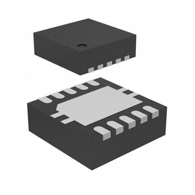
| 描述 | IC REG BUCK SYNC 1.6V 0.5A 10SON |
| 产品分类 | |
| 品牌 | Texas Instruments |
| 数据手册 | |
| 产品图片 |
|
| 产品型号 | TPS62302DRCR |
| PCN设计/规格 | |
| PWM类型 | 电压模式 |
| rohs | 无铅 / 符合限制有害物质指令(RoHS)规范要求 |
| 产品系列 | - |
| 产品目录页面 | |
| 供应商器件封装 | 10-SON(3x3) |
| 其它名称 | 296-18982-6 |
| 包装 | Digi-Reel® |
| 参考设计库 | http://www.digikey.com/rdl/4294959904/4294959903/305 |
| 同步整流器 | 是 |
| 安装类型 | 表面贴装 |
| 封装/外壳 | 10-VFDFN 裸露焊盘 |
| 工作温度 | -40°C ~ 85°C |
| 标准包装 | 1 |
| 电压-输入 | 2.7 V ~ 6 V |
| 电压-输出 | 1.6V |
| 电流-输出 | 500mA |
| 类型 | 降压(降压) |
| 输出数 | 1 |
| 输出类型 | 固定 |
| 配用 | /product-detail/zh/TPS62300EVM-085/296-18981-ND/863803 |
| 频率-开关 | 3MHz |


- 商务部:美国ITC正式对集成电路等产品启动337调查
- 曝三星4nm工艺存在良率问题 高通将骁龙8 Gen1或转产台积电
- 太阳诱电将投资9.5亿元在常州建新厂生产MLCC 预计2023年完工
- 英特尔发布欧洲新工厂建设计划 深化IDM 2.0 战略
- 台积电先进制程称霸业界 有大客户加持明年业绩稳了
- 达到5530亿美元!SIA预计今年全球半导体销售额将创下新高
- 英特尔拟将自动驾驶子公司Mobileye上市 估值或超500亿美元
- 三星加码芯片和SET,合并消费电子和移动部门,撤换高东真等 CEO
- 三星电子宣布重大人事变动 还合并消费电子和移动部门
- 海关总署:前11个月进口集成电路产品价值2.52万亿元 增长14.8%


PDF Datasheet 数据手册内容提取
TPS62300, TPS62301, TPS62302 QFN-10 CSP-8 TPS62303, TPS62304, TPS62305, TPS62311, TPS62313, TPS62315, TPS62320, TPS62321 www.ti.com SLVS528E–JULY2004–REVISEDNOVEMBER2007 500-mA, 3-MHz SYNCHRONOUS STEP-DOWN CONVERTER IN CHIP SCALE PACKAGING FEATURES 1 • Upto93%Efficiencyat3-MHzOperation 234 DESCRIPTION • Upto500-mAOutputCurrentatV =2.7V I The TPS623xx device is a high-frequency • 3-MHzFixedFrequencyOperation synchronous step-down dc-dc converter optimized for • BestinClassLoadandLineTransient battery-powered portable applications. Intended for • Complete1-mmComponentProfileSolution low-power applications, the TPS623xx supports up to • -0.5%/+1.3%PWMDCVoltageAccuracyOver 500-mA load current and allows the use of tiny, low costchipinductorandcapacitors. Temperature • 35-nsMinimumOn-Time The device is ideal for mobile phones and similar portable applications powered by a single-cell Li-Ion • Power-SaveModeOperationatLightLoad battery or by 3-cell NiMH/NiCd batteries. With an Currents output voltage range from 5.4 V down to 0.6 V, the • FixedandAdjustableOutputVoltage device supports the low-voltage TMS320™ DSP • Only86-m AQuiescentCurrent family, processors in smart-phones, PDAs as well as notebooks,andhandheldcomputers. • 100%DutyCycleforLowestDropout • SynchronizableOntheFlytoExternal The TPS62300 operates at 3-MHz fixed switching frequency and enters the power-save mode operation ClockSignal at light load currents to maintain high efficiency over • IntegratedActivePower-DownSequencing the entire load current range. For low noise (TPS6232xonly) applications, the device can be forced into fixed • Availableina10-PinQFN(3x3mm),8-Pin frequency PWM mode by pulling the MODE/SYNC NanoFree™,andNanoStar™(CSP)Packaging pin high. The device can also be synchronized to an external clock signal in the range of 3 MHz. In the shutdown mode, the current consumption is reduced APPLICATIONS tolessthan1m A. • CellPhones,Smart-Phones • WLANandBluetooth™Applications The TPS623xx is available in a 10-pin leadless package (3 x 3 mm QFN) and an 8-pin chip-scale • MicroDC-DCConverterModules package(CSP). • PDAs,PocketPCs • USB-BasedDSLModems 100 • DigitalCameras 90 VVIO = = 3 1.6.8 V V, 80 2V.7I V . 4. .67C Vm1F CAB122 VEMINONTDPES/6S2Y3N03CVYOAZSUDDWTJ DCB121 1 mLH1 C42.7 mV1F.O8 V/500 mA Efficiency − % 45670000 A1 GND FB D2 30 20 Figure1.SmallestSolutionSizeApplication L = 2.2 m H, (FixedOutputVoltage) 10 CO = 4.7 m F 0 0.1 1 10 100 1 k IO − Load Current − mA Figure2.EfficiencyvsLoadCurrent 1 Pleasebeawarethatanimportantnoticeconcerningavailability,standardwarranty,anduseincriticalapplicationsof TexasInstrumentssemiconductorproductsanddisclaimerstheretoappearsattheendofthisdatasheet. NanoFree,NanoStar,TMS320aretrademarksofTexasInstruments. 2 BluetoothisatrademarkofBluetoothSIG,Inc. 3 PowerPADisatrademarkofTexasInstsruments. 4 PRODUCTIONDATAinformationiscurrentasofpublicationdate. Copyright©2004–2007,TexasInstrumentsIncorporated Products conform to specifications per the terms of the Texas Instruments standard warranty. Production processing does not necessarilyincludetestingofallparameters.
TPS62300, TPS62301, TPS62302 TPS62303, TPS62304, TPS62305, TPS62311, TPS62313, TPS62315, TPS62320, TPS62321 www.ti.com SLVS528E–JULY2004–REVISEDNOVEMBER2007 Thesedeviceshavelimitedbuilt-inESDprotection.Theleadsshouldbeshortedtogetherorthedeviceplacedinconductivefoam duringstorageorhandlingtopreventelectrostaticdamagetotheMOSgates. ORDERINGINFORMATION TA NUPMARBTER VOOULTTPAUGTE UNDLEORCVKOOLUTTAGE PACKAGE ORDERING(1)(2) PMAACRKKAINGGE 2.4V QFN-10 TPS62300DRC AMN TPS62300 Adjustable 2.4V CSP-8 TPS62300YZD N/A 2.4V QFN-10 TPS62301DRC AMO TPS62301 1.5V 2.4V CSP-8 TPS62301YZD N/A 2.4V QFN-10 TPS62302DRC AMQ TPS62302 1.6V 2.4V CSP-8 TPS62302YZD N/A 2.4V QFN-10 TPS62303DRC AMR TPS62303 1.8V 2.4V CSP-8 TPS62303YZD N/A 2.4V QFN-10 TPS62304DRC AMS TPS62304 1.2V 2.4V CSP-8 TPS62304YZD N/A -40(cid:176)Cto85(cid:176)C 2.4V QFN-10 TPS62305DRC ANU TPS62305 1.875V 2.4V CSP-8 TPS62305YZD N/A TPS62311 1.5V 2V CSP-8 TPS62311YZD N/A TPS62313 1.8V 2V CSP-8 TPS62313YZD N/A TPS62315 1.875V 2V CSP-8 TPS62315YZ N/A 2.4V QFN-10 TPS62320DRC AMX TPS62320 Adjustable 2.4V CSP-8 TPS62320YZD N/A 2.4V CSP-8 TPS62320YED N/A 2.4V QFN-10 TPS62321DRC AMY TPS62321 1.5V 2.4V CSP-8 TPS62321YZD N/A 2.4V CSP-8 TPS62321YED N/A (1) TheYZD,YEDandYZpackagesareavailableintapeandreel.AddaRsuffix(e.g.TPS62300YxDR)toorderquantitiesof3000parts. AddaTsuffix(e.g.TPS62300YxDT)toorderquantitiesof250parts.TheDRCpackageisavailableintapeandreel.AddaRsuffix (e.g.TPS62300DRCR)toorderquantitiesof3000parts. (2) Forthemostcurrentpackageandorderinginformation,seethePackageOptionAddendumattheendofthisdocument,orseetheTI websiteatwww.ti.com. 2 SubmitDocumentationFeedback Copyright©2004–2007,TexasInstrumentsIncorporated ProductFolderLink(s):TPS62300,TPS62301,TPS62302TPS62303,TPS62304,TPS62305,TPS62311,TPS62313, TPS62315,TPS62320,TPS62321
TPS62300, TPS62301, TPS62302 TPS62303, TPS62304, TPS62305, TPS62311, TPS62313, TPS62315, TPS62320, TPS62321 www.ti.com SLVS528E–JULY2004–REVISEDNOVEMBER2007 ABSOLUTE MAXIMUM RATINGS overoperatingfree-airtemperaturerange(unlessotherwisenoted)(1) UNIT VoltageatVIN,AVIN(2) -0.3Vto7V VoltageatSW (2) -0.3Vto7V V VoltageatFB,ADJ -0.3Vto3.6V I VoltageatEN,MODE/SYNC (2) -0.3VtoV +0.3V I VoltageatVOUT(2) 0.3Vto5.4V I Continuousoutputcurrent 500mA O Powerdissipation Internallylimited T Operatingtemperaturerange -40(cid:176) Cto85(cid:176) C A T (max) Maximumoperatingjunctiontemperature 150(cid:176) C J T Storagetemperaturerange -65(cid:176) Cto150(cid:176) C stg HumanbodymodelatAVIN,FB,ADJ,EN,MODE_SYNC,VOUT 2kV ESD rating(3) HumanbodymodelatVIN,SW 1kV Chargedevicemodel 1.5kV (1) Stressesbeyondthoselistedunder"absolutemaximumratings"maycausepermanentdamagetothedevice.Thesearestressratings onlyandfunctionaloperationofthedeviceattheseoranyotherconditionsbeyondthoseindicatedunder"recommendedoperating conditions"isnotimplied.Exposuretoabsolute-maximum-ratedconditionsforextendedperiodsmayaffectdevicereliability. (2) Allvoltagevaluesarewithrespecttonetworkgroundterminal. (3) Thehumanbodymodelisa100-pFcapacitordischargedthrougha1.5-kΩresistorintoeachpin. Copyright©2004–2007,TexasInstrumentsIncorporated SubmitDocumentationFeedback 3 ProductFolderLink(s):TPS62300,TPS62301,TPS62302TPS62303,TPS62304,TPS62305,TPS62311,TPS62313, TPS62315,TPS62320,TPS62321
TPS62300, TPS62301, TPS62302 TPS62303, TPS62304, TPS62305, TPS62311, TPS62313, TPS62315, TPS62320, TPS62321 www.ti.com SLVS528E–JULY2004–REVISEDNOVEMBER2007 DISSIPATION RATINGS(1) PACKAGE Rq JA(2) PFOOWRETRR≤A2T5(cid:176)INCG DAEBROATVIENGT F=A2C5T(cid:176)OCR A A DRC 49(cid:176) C/W 2050mW 21mW/(cid:176) C YZD 250(cid:176) C/W 400mW 4mW/(cid:176) C YED 250(cid:176) C/W 400mW 4mW/(cid:176) C YZ 250(cid:176) C/W 400mW 4mW/(cid:176) C (1) MaximumpowerdissipationisafunctionofT(max),q andT .Themaximumallowablepowerdissipationatanyallowableambient J JA A temperatureisP =[T(max)-T ]/q D J A JA (2) Thisthermaldataismeasuredwithlow-Kboard(1layerboardaccordingtoJESD51-7JEDECstandard). ELECTRICAL CHARACTERISTICS V =3.6V,V =1.6V,EN=V,MODE/SYNC=GND,L=1m H,C =10m F,T =-40(cid:176) Cto85(cid:176) C,typicalvaluesareat I O I O A T =25(cid:176) C(unlessotherwisenoted) A PARAMETER TESTCONDITIONS MIN TYP MAX UNIT SUPPLYCURRENT VI Inputvoltagerange 2.7 6 V TTPPSS66223302xx IO=0mA.PFMmodeenabled,devicenotswitching 86 105 m A IQ Oqupieersacteinngt TPS6231x IO=0mA.PFMmodeenabled,devicenotswitching 86 120 m A current TPS6230x TPS6231x IO=0mA.Switchingwithnoload 3.6 mA (MODE/SYNC=VIN) TPS6232x I(SD) Shutdowncurrent EN=GND 0.1 1 m A TPS6230x UVLO Undervoltage TPS6232x 2.40 2.55 V lockoutthreshold TPS6231x 2.00 2.20 V ENABLE,MODE/SYNC V(EN) ENhigh-levelinputvoltage 1.2 V V(MODE/SYNC) MODE/SYNChigh-levelinputvoltage 1.3 V V(EN), EN,MODE/SYNClow-levelinput 0.4 V V(MODE/SYNC) voltage I(EN), EN,MODE/SYNCinputleakage EN,MODE/SYNC=GNDorVIN 0.01 1 m A I(MODE/SYNC) current POWERSWITCH P-channelMOSFET TPS6230x VI=V(GS)=3.6V 420 750 mΩ rDS(on) onresistance TTPPSS66223312xx VI=V(GS)=2.8V 520 1000 mΩ Ilkg P-channelleakagecurrent,PMOS V(DS)=6V 1 m A VI=V(GS)=3.6V 330 750 mΩ rDS(on) N-channelMOSFETonresistance VI=V(GS)=2.8V 400 1000 mΩ Dischargeresistorforpower-down R(DIS) sequence(TPS6232xonly) 30 50 Ω Ilkg N-channelleakagecurrent,NMOS V(DS)=6V 1 m A P-MOScurrentlimit 2.7V≤VI≤6V 670 780 890 mA N-MOScurrentlimit-sourcing 2.7V≤VI≤6V 550 720 890 mA N-MOScurrentlimit-sinking 2.7V≤VI≤6V –460 –600 –740 mA Inputcurrentlimitundershort-circuit conditions VO=0V 390 mA Thermalshutdown 150 (cid:176)C Thermalshutdownhysteresis 20 (cid:176)C 4 SubmitDocumentationFeedback Copyright©2004–2007,TexasInstrumentsIncorporated ProductFolderLink(s):TPS62300,TPS62301,TPS62302TPS62303,TPS62304,TPS62305,TPS62311,TPS62313, TPS62315,TPS62320,TPS62321
TPS62300, TPS62301, TPS62302 TPS62303, TPS62304, TPS62305, TPS62311, TPS62313, TPS62315, TPS62320, TPS62321 www.ti.com SLVS528E–JULY2004–REVISEDNOVEMBER2007 ELECTRICAL CHARACTERISTICS (continued) V =3.6V,V =1.6V,EN=V,MODE/SYNC=GND,L=1m H,C =10m F,T =-40(cid:176) Cto85(cid:176) C,typicalvaluesareat I O I O A T =25(cid:176) C(unlessotherwisenoted) A PARAMETER TESTCONDITIONS MIN TYP MAX UNIT OSCILLATOR fSW Oscillatorfrequency 2.65 3 3.35 MHz f(SYNC) Synchronizationrange 2.65 3.35 MHz Dutycycleofexternalclocksignal 20% 80% OUTPUT Adjustableoutput TPS62300 VO voltagerange TPS62320 0.6 5.4 V Regulatedfeedback TPS62300 V(FB) voltage TPS62320 0.4 V DCpowertrainamplification A(PT) (VO/V(ADJ)) 1.496 1.5 1.504 Minimumon-time(P-channel ton(MIN) MOSFET) 35 ns ResistanceintoVOUTsensepin 700 1000 kΩ ResistanceintoADJpin V(FB)>0.4V 700 1000 1300 kΩ Feedbackinputbias TPS62300 I(FB) current TPS62320 V(FB)=0.4V 1 nA Adjustableoutput TPS62300 voltage(1) TPS62320 –2% +2% TPS6230x TPS62311 TPS62313 2.7V≤VI ≤6V,0mA≤IO(DC)≤500mA –2% +2% TPS6232x PFM/PWMmodeoperation Fixedoutputvoltage TPS62304 -2% +2.5% TPS62305 –2% +2.7% TPS62315 VO Avodljtuasgteabdlceaocuctpuuratcy(1) TTPPSS6622330200 T–4A0=(cid:176)C25≤(cid:176)CTA≤85(cid:176)C ––00..55%% ++11..33%% TPS6230x TA=25(cid:176)C –0.5% +1.3% TPS62311 TTPPSS662233123x PWMmodeoperation, –40(cid:176)C≤TA≤85(cid:176)C –0.5% +1.3% Fdcixeadccouuratpcuytvoltage TPS62304 VI=3.6V,NoLoad TA=25(cid:176)C -0.5% +1.8% –40(cid:176)C≤TA≤85(cid:176)C -0.5% +1.8% TPS62305 TA=25(cid:176)C –0.3% +1.7% TPS62315 –40(cid:176)C≤TA≤85(cid:176)C –0.5% +2% DCoutputvoltageloadregulation IO=0mAto500mA,MODE/SYNC=VI –0.001 –0.002 %/mA DCoutputvoltageloadregulation V(ADJ)externallyforcedto1.067V, –0.0003 –0.0006 %/mA (powertrainindirectdrivemode) IO=0mAto500mA,MODE/SYNC=VI DCoutputvoltagelineregulation VI=VO+0.5V(min2.7V)to 0.11 0.2 %/V 6V,IO=100mA,MODE/SYNC=VI DCoutputvoltagelineregulation V(ADJ)externallyforcedto1.067V, (powertrainindirectdrivemode) VI=VO+0.5V(min2.7V)to6V 0.035 0.1 %/V IO=100mA,MODE/SYNC=VI Integratorslewrate 100 150 200 m V/m s ΔVO Power-savemoderipplevoltage IO=1mA,MODE/SYNC=GND 0.025VO VP-P Start-uptime IO=200mA,TimefromactiveENtoVO 250 m s Ilkg LeakagecurrentintoSWpin VI>VO,0V≤V(SW)≤VIN,EN=GND 0.1 1 m A ReverseleakagecurrentintoSWpin VI=open,V(SW)=6V,EN=GND 0.1 1 (1) Outputvoltagespecificationfortheadjustableversiondoesnotincludetoleranceofexternalvoltageprogrammingresistors. Copyright©2004–2007,TexasInstrumentsIncorporated SubmitDocumentationFeedback 5 ProductFolderLink(s):TPS62300,TPS62301,TPS62302TPS62303,TPS62304,TPS62305,TPS62311,TPS62313, TPS62315,TPS62320,TPS62321
TPS62300, TPS62301, TPS62302 TPS62303, TPS62304, TPS62305, TPS62311, TPS62313, TPS62315, TPS62320, TPS62321 www.ti.com SLVS528E–JULY2004–REVISEDNOVEMBER2007 PIN ASSIGNMENTS TPS62300, TPS62320 TPS6230x, TPS6232x QFN-10 FIXED OUTPUT VOLTAGE (QFN-10) (TOPVIEW) (TOPVIEW) VIN SW VIN SW AVIN PGND AVIN PGND EN MODE/SYNC EN MODE/SYNC ADJ AGND NC AGND FB VOUT NC VOUT TPS6230x, TPS6231x, TPS6232x TPS6230x, TPS6231x, TPS6232x CSP-8 CSP-8 (TOPVIEW) (BOTTOM VIEW) GND A1 A2 VIN VIN A2 A1 GND SW B1 B2 EN EN B2 B1 SW MODE/SYNC C1 C2 ADJ ADJ C2 C1 MODE/SYNC VOUT D1 D2 FB FB D2 D1 VOUT TERMINALFUNCTIONS TERMINAL NO. NO. I/O DESCRIPTION NAME QFN CSP VIN 1 A2 I Supplyvoltageforoutputpowerstage. AVIN 2 I Thisistheinputvoltagepinofthedevice.Connectdirectlytotheinputbypasscapacitor. Thisistheenablepinofthedevice.Connectingthispintogroundforcesthedeviceintoshutdown EN 3 B2 I mode.PullingthispintoV enablesthedevice.Thispinmustnotbeleftfloatingandmustbe I terminated. ThisistheinternalreferencevoltageusedtoregulateV .Thispinisnotconnectedonfixedoutput O voltageversionofTPS6230xDRCandTPS6232xDRC.DonotconnectADJpinonfixedoutput ADJ 4 C2 I/O voltageversionofTPS6230xYZD,TPS6231xYZD,TPS6231xYZandTPS6232xYxD. OnTPS62300andTPS62320,thispincanalsobeusedasanexternalcontrolinput.Theoutput voltageis1.5xtheappliedvoltageatADJ. Thisisthefeedbackpinofthedevice.Fortheadjustableversion,anexternalresistordivideris connectedtothispin.Theinternalvoltagedividerisdisabledfortheadjustableversion.Thispinis FB 5 D2 I notconnectedonfixedoutputvoltageversionofTPS6230xDRCandTPS6232xDRC.Donot connecttheFBpinonthefixedoutputvoltageversionofTPS6230xYZD,TPS6231xYZD, TPS6231xYZandTPS6232xYxD. VOUT 6 D1 I Outputfeedbacksenseinput.ConnectVOUTtotheconverter’soutput. AGND 7 Analogground.ConnecttoPGNDviathePowerPAD™underneathIC. Inputforsynchronizationtoexternalclocksignal.Thispinmustnotbeleftfloatingandmustbe terminated.Synchronizestheconverterswitchingfrequencytoanexternalclocksignal MODE/SYNC=LOW(GND):Thedeviceisoperatinginfixedfrequencypulsewidthmodulation MODE/SYNC 8 C1 I mode(PWM)athigh-loadcurrentsandinpulsefrequencymodulationmode(PFM)atlightload currents. MODE/SYNC=HIGH(VIN):Low-noisemodeenabled,fixedfrequencyPWMoperationforced. PGND 9 A1 Powerground. ThisistheswitchpinoftheconverterandisconnectedtothedrainoftheinternalPower SW 10 B1 I/O MOSFETs. PowerPAD™ N/A InternallyconnectedtoPGND. 6 SubmitDocumentationFeedback Copyright©2004–2007,TexasInstrumentsIncorporated ProductFolderLink(s):TPS62300,TPS62301,TPS62302TPS62303,TPS62304,TPS62305,TPS62311,TPS62313, TPS62315,TPS62320,TPS62321
TPS62300, TPS62301, TPS62302 TPS62303, TPS62304, TPS62305, TPS62311, TPS62313, TPS62315, TPS62320, TPS62321 www.ti.com SLVS528E–JULY2004–REVISEDNOVEMBER2007 FUNCTIONAL BLOCK DIAGRAM MODE/SYNC EN VIN Undervoltage N-MOS Current Limit AVIN Lockout Compator Bias Supply _ VREF= 0.4 V Soft-Start Band Gap Power-Save REF 3-MHz Mode + Oscillator + PLL Thermal Sawtooth Shutdown Generator Comp Low Switching + Logic _ REF : RAMPHEIGHT P-MOS Current Limit 0.1 VIN Compator 2R C R - VOUT - - ++ - SW Gate Driver 2C R(DIS) - Anti VREF _+ + + + ++ Summing Shoot-Through EN FB A(DC)= 3 Comparator Mid-, High-Frequency TPS6232x P Zero-Pole Pair PP Only A R2 R1 VOUT See noteA ADJ Comparator Low + A -1.5% VOUT(NOMINAL) _ AGND PGND NOTEA: PARAMETER MEASUREMENT INFORMATION U1 1 VIN SW 10 L1 VO 2.7 V . . 6 V 2 6 C2 1.6 V/500 mA AVIN VOUT C1 3 4 R1 10mF VI EN ADJ 8 5 MODE/SYNCFB 7 AGND PGND 9 R2 A A A List of Components: U1 = TPS6230x L1 = FDK MIPW3226 Series C1, C2 = X5R/X7R Copyright©2004–2007,TexasInstrumentsIncorporated SubmitDocumentationFeedback 7 ProductFolderLink(s):TPS62300,TPS62301,TPS62302TPS62303,TPS62304,TPS62305,TPS62311,TPS62313, TPS62315,TPS62320,TPS62321
TPS62300, TPS62301, TPS62302 TPS62303, TPS62304, TPS62305, TPS62311, TPS62313, TPS62315, TPS62320, TPS62321 www.ti.com SLVS528E–JULY2004–REVISEDNOVEMBER2007 TYPICAL CHARACTERISTICS Table of Graphs FIGURE vsLoadcurrent 3,4,5,6 h Efficiency vsInputvoltage 7 Linetransientresponse 8 9,10,11,12, Loadtransientresponse 13,14,15,16 V DCoutputvoltage vsLoadcurrent 17 O V Regulatedfeedbackvoltage vsTemperature 18 FB I Noloadquiescentcurrent vsInputvoltage 19 Q f Switchingfrequency vsTemperature 20 s Dutycyclejitter 21 P-channelMOSFETr vsInputvoltage 22 DS(on) r DS(on) N-channelMOSFETr vsInputvoltage 23 DS(on) PWMoperation 24 Power-savemodeoperation 25 Dynamicvoltagemanagement 26,27 Start-up 28,29 Powerdown(TPS6232x) 30 EFFICIENCY EFFICIENCY vs vs LOADCURRENT LOADCURRENT 100 100 VI = 3.6 V, PFM/PWM Operation VI = 3.6 V, PFM/PWM Operation 90 VO = 1.8 V L = 2.2 (cid:1)H 90 VO = 1.6 V L = 2.2 (cid:1)H 80 80 70 70 PFM/PWM Operation % L = 0.9 (cid:1)H % y − 60 y − 60 PWM Operation c c L = 0.9 (cid:1)H n 50 n 50 e e ci ci Effi 40 PWM Operation Effi 40 L = 2.2 (cid:1)H 30 30 20 20 10 10 0 0 0.1 1 10 100 1000 0.1 1 10 100 1000 IO − Load Current − mA IO − Load Current − mA Figure3. Figure4. 8 SubmitDocumentationFeedback Copyright©2004–2007,TexasInstrumentsIncorporated ProductFolderLink(s):TPS62300,TPS62301,TPS62302TPS62303,TPS62304,TPS62305,TPS62311,TPS62313, TPS62315,TPS62320,TPS62321
TPS62300, TPS62301, TPS62302 TPS62303, TPS62304, TPS62305, TPS62311, TPS62313, TPS62315, TPS62320, TPS62321 www.ti.com SLVS528E–JULY2004–REVISEDNOVEMBER2007 EFFICIENCY EFFICIENCY vs vs LOADCURRENT LOADCURRENT 90 100 PFM/PWM Operation PFM/PWM Operation 80 L = 2.2 (cid:1)H 90 L = 2.2 (cid:1)H 80 70 70 60 % % y − 50 PL W= M2. 2O (cid:1)pHeration cy − 60 nc en 50 PWM Operation Efficie 40 Effici 40 L = 0.9 (cid:1)H 30 30 20 20 10 VI = 3.6 V, 10 VI = 5 V, VO = 1.2 V VO = 3.3 V 0 0 0.1 1 10 100 1000 0.1 1 10 100 1000 IO − Load Current − mA IO − Load Current − mA Figure5. Figure6. EFFICIENCY vs INPUTVOLTAGE LINETRANSIENTRESPONSE 100 90 IO = 100 mA IO = 400 mA Offset VO = 1.6 V L = 0.9 (cid:1)H, CO = 10 (cid:1)F V 80 6 3. − 70 v % IO = 1 mA di ciency − 5600 IO = 10 mA V= 1 V/I Offset Effi 40 6 V 1. − 30 v di 20 PFM/PWM Operation mV/ 10 VO = 1.8 V = 10 O 0 V 2.7 3 3.3 3.6 3.9 4.2 4.5 4.8 5.1 5.4 5.7 6 t − Time − 100 (cid:1)s/div VI − Input Voltage − V Figure7. Figure8. Copyright©2004–2007,TexasInstrumentsIncorporated SubmitDocumentationFeedback 9 ProductFolderLink(s):TPS62300,TPS62301,TPS62302TPS62303,TPS62304,TPS62305,TPS62311,TPS62313, TPS62315,TPS62320,TPS62321
TPS62300, TPS62301, TPS62302 TPS62303, TPS62304, TPS62305, TPS62311, TPS62313, TPS62315, TPS62320, TPS62321 www.ti.com SLVS528E–JULY2004–REVISEDNOVEMBER2007 LOADTRANSIENTRESPONSEIN LOADTRANSIENTRESPONSEIN PWMOPERATION PWMOPERATION mA/div VVIO = = 3 1.6.6 V V, ML O= D0.E9/ S(cid:1)HYN, CCO = = H 1IG0 H(cid:1)F mA/div VVIO = = 3 1.6.6 V V, mA or 200 mA or 200 ML O= D0.E9/ S(cid:1)HYN, CCO = = H 1IG0 H(cid:1)F I= 50 O IO = 10 to 100 mA Load Step Offset I= 50 O IO = 10 to 100 mA Load Step Offset V V 6 6 1. 1. − − v v di di V/ V/ m m IO = 10 to 400 mA Load Step 0 0 1 1 = IO = 10 to 400 mA Load Step = O O V V t − Time − 50 (cid:1)s/div t − Time − 2 (cid:1)s/div Figure9. Figure10. LOADTRANSIENTRESPONSEIN LOADTRANSIENTRESPONSE PWMOPERATION INPFMMODE v VI = 3.6 V, MODE/SYNC = HIGH VI = 3.6 V, L = 0.9 (cid:1)H, CO = 10 (cid:1)F A/di VO = 1.6 V L = 0.9 (cid:1)H, CO = 10 (cid:1)F div VO = 1.6 V m A/ 0 m mA or 20 = 100 O 0 I 5 I= O IO = 400 to 10 mA Load Step Offset Offset V V v - 1.6 v − 1.6 di di V/ V/ m m IO = 100 to 10 mA Load Step 10 20 = PFM Operation = O O V V t - Time - 2 (cid:1)s/div t − Time − 50 (cid:1)s/div Figure11. Figure12. 10 SubmitDocumentationFeedback Copyright©2004–2007,TexasInstrumentsIncorporated ProductFolderLink(s):TPS62300,TPS62301,TPS62302TPS62303,TPS62304,TPS62305,TPS62311,TPS62313, TPS62315,TPS62320,TPS62321
TPS62300, TPS62301, TPS62302 TPS62303, TPS62304, TPS62305, TPS62311, TPS62313, TPS62315, TPS62320, TPS62321 www.ti.com SLVS528E–JULY2004–REVISEDNOVEMBER2007 LOADTRANSIENTRESPONSEIN LOADTRANSIENTRESPONSEIN PWMOPERATION PWMOPERATION mA/div VVIO = = 3 1.6.6 V V, ML O= D0.E9/ (cid:1)SHY,N CCO = = H 4I.G7 H(cid:1)F mA/div VVIO = = 3 1.6.6 V V, or 200 or 200 ML O= D0.E9/ (cid:1)SHY,N CCO = = H 4I.G7 H(cid:1)F A A m m I = 50 O IO = 10 to 100 mA Load Step Offset I = 50 O IO = 10 to 100 mA Load Step Offset V V div - 1.6 div - 1.6 V/ V/ IO = 10 to 400 mA Load Step = 10 m IO = 10 to 400 mA Load Step = 20 m O O V V t - Time - 50 (cid:1)s/div t - Time - 2 (cid:1)s/div Figure13. Figure14. LOADTRANSIENTRESPONSEIN LOADTRANSIENTRESPONSEIN PFMOPERATION PFMOPERATION 0 mA/div VVIO = = 3 1.6.6 V V, ML O= D0.E9/ (cid:1)SHY,N CCO = = H 4I.G7 H(cid:1)F mA/div VVIO = = 3 1.6.6 V V, L = 0.9 (cid:1)H, CO = 4.7 (cid:1)F 0 2 0 or 10 A = m O 0 I 5 = O et et I s s IO = 400 to 10 mA Load Step Off Off V V 6 6 1. 1. v - v - di di V/ V/ m m 0 0 IO = 100 to 10 mA Load Step = 2 PFM Operation = 2 O O V V t - Time - 2 (cid:1)s/div t - Time - 50 (cid:1)s/div Figure15. Figure16. Copyright©2004–2007,TexasInstrumentsIncorporated SubmitDocumentationFeedback 11 ProductFolderLink(s):TPS62300,TPS62301,TPS62302TPS62303,TPS62304,TPS62305,TPS62311,TPS62313, TPS62315,TPS62320,TPS62321
TPS62300, TPS62301, TPS62302 TPS62303, TPS62304, TPS62305, TPS62311, TPS62313, TPS62315, TPS62320, TPS62321 www.ti.com SLVS528E–JULY2004–REVISEDNOVEMBER2007 OUTPUTVOLTAGE REGULATEDFEEDBACKVOLTAGE vs vs LOADCURRENT TEMPERATURE 1.628 406 VI = 3.6 V, VO = 1.6 V, L = 2.2 (cid:1)H TPS62300 V 405.5 1.618 m V e - − ag 405 ge 1.608 PWM Operation olt a V put Volt 1.598 edback 40440.45 VI = 4.2 V VI = 3.6 V V− OutO 1.588 PFM/PWM Operation ulated Fe 403.5 g Re 403 1.578 - B) VI = 2.7 V V(F 402.5 1.568 402 0.1 1 10 100 1000 -40 -30 -20 -10 0 10 20 30 40 50 60 70 80 85 IO − Load Current − mA TA - Ambient Temperature - (cid:1)C Figure17. Figure18. QUIESCENTCURRENT OSCILLATORFREQUENCY vs vs INPUTVOLTAGE INPUTVOLTAGE 96 3.3 94 3.25 z H M murrent − A 9902 TA = 85(cid:1)C TA = 25(cid:1)C equency − 33.1.25 TTAA == −254(cid:1)0C(cid:1)C C r nt 88 r F 3.1 e o uiesc 86 scillat 3.05 TA = 85(cid:1)C Q O − − IQ 84 TA = −40(cid:1)C fs 3 MODE/SYNC = HIGH 82 2.95 2.9 80 2.7 3 3.3 3.6 3.9 4.2 4.5 4.8 5.1 5.4 5.7 6 2.7 3 3.3 3.6 3.9 4.2 4.5 4.8 5.1 5.4 5.7 6 V − Input Voltage − V VI − Input Voltage − V I Figure19. Figure20. 12 SubmitDocumentationFeedback Copyright©2004–2007,TexasInstrumentsIncorporated ProductFolderLink(s):TPS62300,TPS62301,TPS62302TPS62303,TPS62304,TPS62305,TPS62311,TPS62313, TPS62315,TPS62320,TPS62321
TPS62300, TPS62301, TPS62302 TPS62303, TPS62304, TPS62305, TPS62311, TPS62313, TPS62315, TPS62320, TPS62321 www.ti.com SLVS528E–JULY2004–REVISEDNOVEMBER2007 P-CHANNELr DS(ON) vs DUTYCYCLEJITTER INPUTVOLTAGE 700 VI = 3.6 V, VO = 1.6 V, L = 0.9 (cid:1)H, CO = 10 (cid:1)F Wm 650 − e 600 TRIGGER ON RISING EDGE IO = 320 mA stanc 550 TA = 85(cid:1)C si div n-Re 500 TA = 25(cid:1)C V/ O 450 W - 1 urce 400 o S S n- 350 Drai 300 TA = −40(cid:1)C c Stati 250 − MODE/SYNC = HIGH n) 200 o S( 150 D r 2.5 3 3.5 4 4.5 5 5.5 6 t - Time - 25 ns/div VI − Input Voltage − V Figure21. Figure22. N-CHANNELr DS(ON) vs INPUTVOLTAGE PWMOPERATION 550 v Wm A/di IO = 200 mA L = 0.9 (cid:1)H, CO = 10 (cid:1)F − m Resistance 455000 TA = 85(cid:1)C I − 200 L n- 400 O v e di n-Sourc 350 TA = 25(cid:1)C W − 2 V/ V Offset ai 300 S 6 Dr 1. Static 250 V/div − − TA = −40(cid:1)C m n) 200 0 S(o VI = 3.6 V, VO = 1.6 V − 1 D O r 150 V 2.5 3 3.5 4 4.5 5 5.5 6 t − Time − 200 ns/div VI − Input Voltage − V Figure23. Figure24. Copyright©2004–2007,TexasInstrumentsIncorporated SubmitDocumentationFeedback 13 ProductFolderLink(s):TPS62300,TPS62301,TPS62302TPS62303,TPS62304,TPS62305,TPS62311,TPS62313, TPS62315,TPS62320,TPS62321
TPS62300, TPS62301, TPS62302 TPS62303, TPS62304, TPS62305, TPS62311, TPS62313, TPS62315, TPS62320, TPS62321 www.ti.com SLVS528E–JULY2004–REVISEDNOVEMBER2007 POWER-SAVEMODEOPERATION DYNAMICVOLTAGEMANAGEMENT v v VI = 3.6 V, A/di V/di VO = 1 V / 1.5 V VO = 1.5 V m m 0 0 0 0 2 2 − − I L VO VO = 1 V v et V(ADJ) = 0.67 V V(ADJ) = 1 V A/di s m Off 0 V 50 6 − 1. J v − div AD di A/ V/ m m 0 − 20 VO VIOI == 34.06 mV,A VO = 1.6 V L = 0.9 (cid:1)H, CO = 10 (cid:1)F I − 50L LM O= D0.E9/ S(cid:2)HYN, CCO = = L 1O0W (cid:2)F, RL = 270 (cid:1) t − Time − 2 (cid:1)s/div t − Time − 20 (cid:2)s/div Figure25. Figure26. DYNAMICVOLTAGEMANAGEMENT START-UP v 0 mV/div VVIO = = 3 1.6 V V /, 1.5 V VO = 1.5 V N − 2 V/di VVIOIO == = 03 1 .m6.6 VA V,, 1 V/div − 20 VO = 1 V E − VO O V v V(ADJ) = 0.67 V V(ADJ) = 1 V A/di div m V/ 00 − 2 5 − DJ J A div AD div V A/ A/ 0 m RL = 5 (cid:1) 0 m 50 L = 0.9 (cid:2)H, CO = 10 (cid:2)F, 20 − MODE/SYNC = HIGH − I L I L L = 2.2 (cid:1)H, CO = 4.7 (cid:1)F, t − Time − 20 (cid:2)s/div t − Time − 50 (cid:1)s/div Figure27. Figure28. 14 SubmitDocumentationFeedback Copyright©2004–2007,TexasInstrumentsIncorporated ProductFolderLink(s):TPS62300,TPS62301,TPS62302TPS62303,TPS62304,TPS62305,TPS62311,TPS62313, TPS62315,TPS62320,TPS62321
TPS62300, TPS62301, TPS62302 TPS62303, TPS62304, TPS62305, TPS62311, TPS62313, TPS62315, TPS62320, TPS62321 www.ti.com SLVS528E–JULY2004–REVISEDNOVEMBER2007 START-UP POWERDOWN(TPS62321) EN − 2 V/div VVIOIO == = 33 12.6.06 V mV,,A − 1 V/div N − 2 V/div VVIOIO == = 03 1 .m6.5 VA V,, E O V v V/di div − 2 mV/ J) 0 D 0 A v 5 V( di − A/ O m V 0 0 2 L = 2.2 (cid:1)H, CO = 4.7 (cid:1)F, I − L L = 0.9 (cid:1)H, CO = 10 (cid:1)F t − Time − 50 (cid:1)s/div t − Time − 400 (cid:1)s/div Figure29. Figure30. DETAILED DESCRIPTION OPERATION The TPS6230x, TPS6231x, and TPS6232x are synchronous step-down converters typically operating with a 3-MHz fixed frequency pulse width modulation (PWM) at moderate to heavy load currents. At light load currents, the converter operates in power-save mode with pulse frequency modulation (PFM). The operating frequency is setto3MHzandcanbesynchronizedon-the-flytoanexternaloscillator. During PWM operation, the converter uses a unique fast response, voltage mode, controller scheme with input voltage feed-forward. This achieves best-in-class load and line response and allows the use of tiny inductors and small ceramic input and output capacitors. At the beginning of each switching cycle, the P-channel MOSFET switch is turned on and the inductor current ramps up until the comparator trips and the control logic turns off the switch. The device integrates two current limits, one in the P-channel MOSFET and another one in the N-channel MOSFET. When the current in the P-channel MOSFET reaches its current limit, the P-channel MOSFET is turned off and the N-channel MOSFET is turned on. When the current in the N-channel MOSFET is above the N-MOS current limit threshold, the N-channel MOSFET remains on until the current drops below its current limit. The current limit in the N-channel MOSFET is important for small duty-cycle operation when the current in the inductor does not decrease because of the P-channel MOSFET current limit delay, or because of start-up conditionswheretheoutputvoltageislow. Copyright©2004–2007,TexasInstrumentsIncorporated SubmitDocumentationFeedback 15 ProductFolderLink(s):TPS62300,TPS62301,TPS62302TPS62303,TPS62304,TPS62305,TPS62311,TPS62313, TPS62315,TPS62320,TPS62321
TPS62300, TPS62301, TPS62302 TPS62303, TPS62304, TPS62305, TPS62311, TPS62313, TPS62315, TPS62320, TPS62321 www.ti.com SLVS528E–JULY2004–REVISEDNOVEMBER2007 POWER-SAVE MODE With decreasing load current, the device automatically switches into pulse skipping operation in which the power stage operates intermittently based on load demand. By running cycles periodically, the switching losses are minimized,andthedevicerunswithaminimumquiescentcurrentandmaintaininghighefficiency. In power-save mode, the converter only operates when the output voltage trips below a set threshold voltage (-1.5% V ). It ramps up the output voltage with several pulses and goes into power-save mode once the O(NOMINAL) output voltage exceeds the nominal output voltage. As a consequence, the average output voltage is slightly lowerthanitsnominalvalueinthepower-savemodeoperation. TheoutputcurrentatwhichthePFM/PWMtransitionoccursisapproximatedbyEquation1: V V (cid:2)V O I O I (cid:3) (cid:1) PFM(cid:4)PWM VI 2 (cid:1) L (cid:1) fsw (1) • I :outputcurrentatwhichPFM/PWMtransitionoccurs PFM/PWM • f :switchingfrequency(3-MHztypical) SW • L:inductorvalue VO(NOMINAL) 3-MHz Operation Comp Low Thershold −1.5% VO(NOMIAL) Figure31.Power-SaveModeThreshold MODE SELECTION AND FREQUENCY SYNCHRONIZATION The MODE/SYNC pin is a multipurpose pin which allows mode selection and frequency synchronization. Connecting this pin to GND enables the automatic PWM and power-save mode operation. The converter operates in fixed frequency PWM mode at moderate to heavy loads and in the PFM mode during light loads, whichmaintainshighefficiencyoverawideloadcurrentrange. Pulling the MODE/SYNC pin high forces the converter to operate in the PWM mode even at light load currents. The advantage is that the converter operates with a fixed frequency that allows simple filtering of the switching frequency for noise-sensitive applications. In this mode, the efficiency is lower compared to the power-save mode during light loads. For additional flexibility, it is possible to switch from power-save mode to forced PWM mode during operation. This allows efficient power management by adjusting the operation of the converter to thespecificsystemrequirements. The TPS6230x, TPS6231x, and TPS6232x can also be synchronized to an external 3-MHz clock signal by the MODE/SYNC pin. During synchronization, the mode is set to fixed-frequency operation and the P-channel MOSFET turnon is synchronized to the falling edge of the external clock. This creates the ability for multiple converters to be connected together in a master-slave configuration for frequency matching of the converters (seetheapplicationsectionformoredetails,Figure37). SOFT START The TPS6230x, TPS6231x, and TPS6232x have an internal soft-start circuit that limits the inrush current during start-up. This prevents possible input voltage drops when a battery or a high-impedance power source is connected to the input of the converter. The soft start is implemented as a digital circuit increasing the switch currentinstepsoftypically195mA,390mA,585mA,andthetypicalswitchcurrentlimitof780mA. The current limit transitions to the next step every 256 clocks (» 88m s). To be able to switch from 390 mA to 585 mA current limit step, the output voltage needs to be higher than 0.5 x V , otherwise, the parts continues to O(NOM) operate at the 390-mA current limit. This mechanism is used to limit the output current under short-circuit conditions.Therefore,thestart-uptimemainlydependsontheoutputcapacitorandloadcurrent. 16 SubmitDocumentationFeedback Copyright©2004–2007,TexasInstrumentsIncorporated ProductFolderLink(s):TPS62300,TPS62301,TPS62302TPS62303,TPS62304,TPS62305,TPS62311,TPS62313, TPS62315,TPS62320,TPS62321
TPS62300, TPS62301, TPS62302 TPS62303, TPS62304, TPS62305, TPS62311, TPS62313, TPS62315, TPS62320, TPS62321 www.ti.com SLVS528E–JULY2004–REVISEDNOVEMBER2007 LOW-DROPOUT OPERATION 100% DUTY CYCLE In 100% duty cycle mode, the TPS6230x, TPS6231x, and TPS6232x offer a low input-to-output voltage difference. In this mode, the P-channel MOSFET is constantly turned on. This is particularly useful in battery-powered applications to achieve the longest operation time by taking full advantage of the whole battery voltage range. The minimum input voltage to maintain regulation, depending on the load current and output voltage,canbecalculatedas: • V =V +I x(r +R ) I(MIN) O(MAX) O(MAX) DS(on)MAX L • I :Maximumoutputcurrent O(MAX) • r :MaximumP-channelswitchr DS(on)MAX DS(on) • R :DCresistanceoftheinductor L • V :nominaloutputvoltageplusmaximumoutputvoltagetolerance O(MAX) ENABLE ThedevicestartsoperationwhenENissethighandstartsupwiththesoftstartaspreviouslydescribed. Pulling the EN pin low forces the device into shutdown, with a shutdown quiescent current of typically 0.1 m A. In this mode, the P and N-channel MOSFETs are turned off, the internal resistor feedback divider is disconnected, and the entire internal-control circuitry is switched off. When an output voltage is present during shutdown mode, which can be caused by an external voltage source or super capacitor, the reverse leakage is specified under electricalcharacteristics.Forproperoperation,theENpinmustbeterminatedandmustnotbeleftfloating. In addition, the TPS6232x devices integrate a resistor, typically 35 Ω, to actively discharge the output capacitor whenthedeviceturnsoff.TherequiredtimetodischargetheoutputcapacitoratV dependsonloadcurrent. O UNDERVOLTAGE LOCKOUT The undervoltage lockout circuit prevents the device from misoperation at low input voltages. It prevents the converterfromturningontheswitchorrectifierMOSFETunderundefinedconditions. The TPS6231x devices have a UVLO threshold set to 2 V (typical). Fully functional operation is permitted down to2.4Vinputvoltage.ENissetlowforinputvoltageslowerthan2.4Vtoavoidthepossibilityofmisoperation. TPS6231x devices are to be considered where the user requires direct control of the turn-off sequence as part of alargerpowermanagementsystem. SHORT-CIRCUIT PROTECTION As soon as the output voltage falls below 50% of the nominal output voltage, the converter current limit is reduced by 50% of the nominal value. Because the short-circuit protection is enabled during start-up, the device does not deliver more than half of its nominal current limit until the output voltage exceeds 50% of the nominal output voltage. This needs to be considered when a load acting as a current sink is connected to the output of theconverter. THERMAL SHUTDOWN As soon as the junction temperature, T , exceeds typically 150(cid:176) C, the device goes into thermal shutdown. In this J mode, the P- and N-channel MOSFETs are turned off. The device continues its operation when the junction temperaturefallsbelowtypically130(cid:176) Cagain. Copyright©2004–2007,TexasInstrumentsIncorporated SubmitDocumentationFeedback 17 ProductFolderLink(s):TPS62300,TPS62301,TPS62302TPS62303,TPS62304,TPS62305,TPS62311,TPS62313, TPS62315,TPS62320,TPS62321
TPS62300, TPS62301, TPS62302 TPS62303, TPS62304, TPS62305, TPS62311, TPS62313, TPS62315, TPS62320, TPS62321 www.ti.com SLVS528E–JULY2004–REVISEDNOVEMBER2007 APPLICATION INFORMATION ADJUSTABLE OUTPUT VOLTAGE When the adjustable output voltage versions, TPS62300 or TPS62320, are used, the output voltage is set by the externalresistordivider(seeFigure32). Theoutputvoltageiscalculatedas: (cid:4) R1(cid:5) VO(cid:3)1.5(cid:1)Vref(cid:1) 1(cid:2)R2 withaninternalreferencevoltageVreftypical(cid:3)0.4V (2) Tokeeptheoperatingquiescentcurrenttoaminimum,itisrecommendedthatR2besetintherangeof75kΩ to 130kΩ.RoutetheFBlineawayfromnoisesources,suchastheinductorortheSWline. TPS62300 L1 1 VIN SW 10 VO 2.7 V . . 6 V C2 1.6 V/500 mA 2 6 AVIN VOUT VI C1 3 EN ADJ 4 R1 4.7mF 4.7mF 8 MODE/SYNCFB 5 7 AGND PGND 9 R2 A A A Figure32.AdjustableOutputVoltageVersion OUTPUT FILTER DESIGN (INDUCTOR AND OUTPUT CAPACITOR) The TPS6230x, TPS6231x, and TPS6232x series of step-down converters have internal loop compensation. Therefore,theexternalL-Cfiltermustbeselectedtoworkwiththeinternalcompensation. Thedevicehasbeendesignedtooperatewithinductancevaluesbetweenaminimumof0.7m Handmaximum of 6.2 m H. The internal compensation is optimized to operate with an output filter of L = 1 m H and C = 10 m F. Such O anoutputfilterhasitscornerfrequencyat: ƒc(cid:2) 1 (cid:2) 1 (cid:2)50.3kHz 2(cid:2)(cid:3)L(cid:1)CO 2(cid:2)(cid:3)1(cid:1)H(cid:1)10(cid:1)F (3) Operation with a higher corner frequency (e.g., L = 1 m H, C = 4.7 m F) is possible. However, it is recommended O the loop stability be checked in detail. Selecting a larger output capacitor value (e.g., 22 m F) is less critical because the corner frequency moves to lower frequencies with fewer stability problems. The possible output filter combinationsarelistedinTable1. Regardless of the inductance value, operation is recommended with 10-m F output capacitor in applications with high-loadtransients(e.g.,≥1600mA/m s). Table1.OutputFilterCombinations INDUCTANCE(L) OUTPUTCAPACITANCE(C ) O 1m H ≥4.7m F(ceramiccapacitor) 2.2m H ≥2.2m F(ceramiccapacitor) The inductor value also has an impact on the pulse skipping operation. The transition into power-save mode begins when the valley inductor current goes below a level set internally. Lower inductor values result in higher ripplecurrentwhichoccursatlowerloadcurrents.Thisresultsinadipinefficiencyatlightloadoperations. 18 SubmitDocumentationFeedback Copyright©2004–2007,TexasInstrumentsIncorporated ProductFolderLink(s):TPS62300,TPS62301,TPS62302TPS62303,TPS62304,TPS62305,TPS62311,TPS62313, TPS62315,TPS62320,TPS62321
TPS62300, TPS62301, TPS62302 TPS62303, TPS62304, TPS62305, TPS62311, TPS62313, TPS62315, TPS62320, TPS62321 www.ti.com SLVS528E–JULY2004–REVISEDNOVEMBER2007 INDUCTOR SELECTION Eventhoughtheinductordoesnotinfluencetheoperatingfrequency,theinductorvaluehasadirect effect on the ripple current. The selected inductor has to be rated for its dc resistance and saturation current. The inductor ripplecurrent(ΔI )decreaseswithhigherinductanceandincreaseswithhigherV orV . L I O V V (cid:3)V (cid:1)I (cid:1)I (cid:4) O(cid:1) I O (cid:1)I (cid:4)I (cid:2) L L V L(cid:1)ƒ L(MAX) O(MAX) 2 I sw (4) with:f =switchingfrequency(3MHztypical) SW L=inductorvalue ΔI =peak-to-peakinductorripplecurrent L I =maximuminductorcurrent L(MAX) Normally, it is advisable to operate with a ripple of less than 30% of the average output current. Accepting larger values of ripple current allows the use of low inductances, but results in higher output voltage ripple, greater core losses,andloweroutputcurrentcapability. The total losses of the coil consist of both the losses in the DC resistance (R ) and the following (DC) frequency-dependentcomponents: • Thelossesinthecorematerial(magnetichysteresisloss,especiallyathighswitchingfrequencies) • Additionallossesintheconductorfromtheskineffect(currentdisplacementathighfrequencies) • Magneticfieldlossesoftheneighboringwindings(proximityeffect) • Radiationlosses The following inductor series from different suppliers have been used with the TPS6230x, TPS6231x, and TPS6232xconverters. Table2.ListofInductors MANUFACTURER SERIES DIMENSIONS FDK MIPW3226 3.2x2.6x1=8.32mm3 MIPSA2520 2.5x2.0x1.2=6mm3 Murata LQM2HP 2.5x2.0x1.2=6mm3 LQCB2016 2x1.6x1.6=5.12mm3 TaiyoYuden LQCB2012 2x1.2x1.2=2.88mm3 LQCBL2012 2x1.2x1=2.40mm3 TDK VLF3010AT 2.8x2.6x1=7.28mm3 Coilcraft LPS3010 3.3x3.3x1=10.89mm3 JFE 32R1560 3.2x2.5x0.6=4.8mm3 OUTPUT CAPACITOR SELECTION The advanced fast-response voltage mode control scheme of the TPS6230x, TPS6231x, and TPS6232x allows the use of tiny ceramic capacitors. Ceramic capacitors with low ESR values have the lowest output voltage ripple and are recommended. The output capacitor requires either an X7R or X5R dielectric. Y5V and Z5U dielectric capacitors,asidefromtheirwidevariationincapacitanceovertemperature,becomeresistiveathighfrequencies. Atnominalloadcurrent,thedeviceoperatesinPWMmodeand the overall output voltage ripple is the sum of the voltagespikecausedbytheoutputcapacitorESRplusthevoltageripplecausedbycharginganddischargingthe outputcapacitor: (cid:1)VO(cid:4)VVOI (cid:1)VLI(cid:1)(cid:3)ƒVsOw (cid:1)(cid:5)8(cid:1)CO1(cid:1)ƒsw(cid:2)ESR(cid:6),maximum for highVI (5) At light loads, the device operates in power-save mode and the output voltage ripple is independent of the output capacitor value. The output voltage ripple is set by the internal comparator thresholds and propagation delays. Thetypicaloutputvoltagerippleis1.5%ofthenominaloutputvoltageV . O Copyright©2004–2007,TexasInstrumentsIncorporated SubmitDocumentationFeedback 19 ProductFolderLink(s):TPS62300,TPS62301,TPS62302TPS62303,TPS62304,TPS62305,TPS62311,TPS62313, TPS62315,TPS62320,TPS62321
TPS62300, TPS62301, TPS62302 TPS62303, TPS62304, TPS62305, TPS62311, TPS62313, TPS62315, TPS62320, TPS62321 www.ti.com SLVS528E–JULY2004–REVISEDNOVEMBER2007 INPUT CAPACITOR SELECTION Because of the nature of the buck converter having a pulsating input current, a low ESR input capacitor is required to prevent large voltage transients that can cause misbehavior of the device or interferences with other circuitsinthesystem.Formostapplications,a2.2-m For4.7-m Fcapacitorissufficient. Take care when using only ceramic input capacitors. When a ceramic capacitor is used at the input and the power is being supplied through long wires, such as from a wall adapter, a load step at the output can induce ringing at the VIN pin. This ringing can couple to the output and be mistaken as loop instability or could even damagethepart. CHECKING LOOP STABILITY Thefirststepofcircuitandstabilityevaluationistolookfromasteady-stateperspectiveatthefollowingsignals: • Switchingnode,SW • Inductorcurrent,I L • Outputripplevoltage,V O(AC) These are the basic signals that need to be measured when evaluating a switching converter. When the switching waveform shows large duty cycle jitter or the output voltage or inductor current shows oscillations, the regulationloopmaybeunstable.Thisisoftenaresultofboardlayoutand/orL-Ccombination. As a next step in the evaluation of the regulation loop, the load transient response is tested. The time between the application of the load transient and the turn on of the P-channel MOSFET, the output capacitor must supply all of the current required by the load. V immediately shifts by an amount equal to ΔI x ESR, where ESR O (LOAD) is the effective series resistance of C . ΔI begins to charge or discharge C generating a feedback error O (LOAD) O signalusedbytheregulatortoreturnV toitssteady-statevalue. O During this recovery time, V can be monitored for settling time, overshoot or ringing that helps judge the O converter’sstability.Withoutanyringing,theloophasusuallymorethan45(cid:176) ofphasemargin. Because the damping factor of the circuitry is directly related to several resistive parameters (e.g., MOSFET r ) that are temperature dependant, the loop stability analysis has to be done over the input voltage range, DS(on) loadcurrentrange,andtemperaturerange. PROGRAMMING THE OUTPUT VOLTAGE WITH A DAC On TPS62300 and TPS62320 devices, the output voltage can be dynamically programmed to any voltage between 0.6 V and V (or 5.4 V whichever is lower) with an external DAC driving the ADJ and FB pins (see I Figure33).TheoutputvoltageisthenequaltoA xV withaPowerTrainamplificationA typical=1.5. (PT) (DAC) (PT) When the output voltage is driven low, the converter reduces its output quickly in forced PWM mode, boosting theoutputenergybacktotheinput.Iftheinputisnotconnectedtoalow-impedancesourcecapableofabsorbing the energy, the input voltage can rise above the absolute maximum voltage of the part and get damaged. The fasterV iscommandedlow,thehigheristhevoltagespikeattheinput. O For best results, ramp the ADJ/FB signal as slow as the application allows. To avoid over-slew of the regulation loop of the converter, avoid abrupt changes in output voltage of > 300 mV/m s (depending on V , output voltage I step size and L/C combination). If ramp control is unavailable, an RC filter can be inserted between the DAC outputandADJ/FBpinstoslowdownthecontrolsignal. TPS62300 VO= 1.5 x V(DAC) L 1 10 VIN SW 2 AVIN VOUT 6 CO VI CI 38 EMNODE/SYNCAFDBJ 45 RF V(DAC) 7 AGND PGND 9 10 kW CF A A A Figure33.FilteringtheDACVoltage 20 SubmitDocumentationFeedback Copyright©2004–2007,TexasInstrumentsIncorporated ProductFolderLink(s):TPS62300,TPS62301,TPS62302TPS62303,TPS62304,TPS62305,TPS62311,TPS62313, TPS62315,TPS62320,TPS62321
TPS62300, TPS62301, TPS62302 TPS62303, TPS62304, TPS62305, TPS62311, TPS62313, TPS62315, TPS62320, TPS62321 www.ti.com SLVS528E–JULY2004–REVISEDNOVEMBER2007 LAYOUT CONSIDERATIONS As for all switching power supplies, the layout is an important step in the design. High-speed operation of the TPS6230x, TPS6231x, and TPS6232x devices demand careful attention to PCB layout. Care must be taken in board layout to get the specified performance. If the layout is not carefully done, the regulator could show poor line and/or load regulation, stability issues as well as EMI problems. It is critical to provide a low inductance, impedance ground path. Therefore, use wide and short traces for the main current paths as indicated in bold on Figure34. The input capacitor should be placed as close as possible to the IC pins as well as the inductor and output capacitor. Use a common ground node for power ground and a different one for control ground (AGND) to minimize the effects of ground noise. Connect these ground nodes together (star point) underneath the IC and make sure that small signal components returning to the AGND pin do not share the high current path of C1 and C2. The output voltage sense line (VOUT) should be connected right to the output capacitor and routed away from noisy components and traces (e.g., SW line). Its trace should be minimized and shielded by a guard-ring connected to the reference ground. The voltage setting resistive divider should be placed as close as possible to theAGNDpinoftheIC. TPS62300 L1 1 VIN SW 10 VO V I 2 6 AVIN VOUT C2 3 4 R1 C1 EN ADJ 8 MODE/SYNC FB 5 7 AGND PGND 9 R2 Figure34.LayoutDiagram GND VO VO sense signal V I EN MODE / SYNC GND Figure36.SuggestedQFNLayout(Bottom) Figure35.SuggestedQFNLayout(Top) Copyright©2004–2007,TexasInstrumentsIncorporated SubmitDocumentationFeedback 21 ProductFolderLink(s):TPS62300,TPS62301,TPS62302TPS62303,TPS62304,TPS62305,TPS62311,TPS62313, TPS62315,TPS62320,TPS62321
TPS62300, TPS62301, TPS62302 TPS62303, TPS62304, TPS62305, TPS62311, TPS62313, TPS62315, TPS62320, TPS62321 www.ti.com SLVS528E–JULY2004–REVISEDNOVEMBER2007 THERMAL INFORMATION Implementation of integrated circuits in low-profile and fine-pitch surface-mount packages typically requires special attention to power dissipation. Many system-dependant issues such as thermal coupling, airflow, added heat sinks, and convection surfaces, and the presence of other heat-generating components, affect the power-dissipationlimitsofagivencomponent Threebasicapproachesforenhancingthermalperformancearelistedbelow: • ImprovingthepowerdissipationcapabilityofthePCBdesign • ImprovingthethermalcouplingofthecomponenttothePCB • Introducingairflowinthesystem The maximum recommended junction temperature (T ) of the TPS6230x, TPS6231x, and TPS6232x devices is J 125(cid:176) C. The thermal resistance of the 8-pin CSP package (YZD, YZ and YED) is Rq JA = 250(cid:176) C/W. Specified regulator operation is specified to a maximum ambient temperature T of 85(cid:176) C. Therefore, the maximum power A dissipation is about 160 mW. More power can be dissipated if the maximum ambient temperature of the applicationislower,orifthePowerPAD™package(DRC)isused. T (cid:1)T J(MAX) A 125°C(cid:1)85°C P (cid:2) (cid:2) (cid:2)160mW D(MAX) R(cid:1)JA 250°C(cid:3)W (6) CHIP SCALE PACKAGE DIMENSIONS The TPS6230x, TPS6231x, and TPS6232x are also available in an 8-bump chip scale package (YZD, YZ NanoFree™andYED,NanoStar™).Thepackagedimensionsaregivenas: • D=1.970±0.05mm • E=0.970±0.05mm 22 SubmitDocumentationFeedback Copyright©2004–2007,TexasInstrumentsIncorporated ProductFolderLink(s):TPS62300,TPS62301,TPS62302TPS62303,TPS62304,TPS62305,TPS62311,TPS62313, TPS62315,TPS62320,TPS62321
TPS62300, TPS62301, TPS62302 TPS62303, TPS62304, TPS62305, TPS62311, TPS62313, TPS62315, TPS62320, TPS62321 www.ti.com SLVS528E–JULY2004–REVISEDNOVEMBER2007 APPLICATION EXAMPLES TPS62303YZD 2.7 V − 6 V A2 VIN VOUT D1 VIN CIN B2 EN SW B1 L1 VOUT Ch1 Ch2 10 mF C1 MODE/SYNC ADJ C2 C1 1.8 V / 500 mA 10 mF A1 GND FB D2 Ch4 TPS62304YZD A2 VIN SW B1 L2 VOUT B2 EN VOUT D1 C2 1.2 V / 500 mA Ch3 10 mF C1 MODE/SYNC ADJ C2 Low: None Synchronized Operation 1G08 A1 GND FB D2 CChh31:: SSWW ((11..82--VV OOuuttppuutt)),, CChh24:: IILL12 PFM/PWM Automatic Switch High: Synchronized Operation Forced 3 MHz Fixed Frequency Operation List of Components: L1, L2 = Taiyo Yuden LQ CB2016 CIN, C1, C2, = X5R/X7R Ceramic Capacitor Figure37.Dual,Out-of-Phase,3-MHz,500-mAStep-DownRegulator FeaturesLessThan50-mm2TotalSolutionSize EN 22 nF 10 kW Fast Start−Up LDO EN EN VOUT(LDO) = 0.98 x VOUT(NOM) VOUT VIN 2.2 MW GND TPS62300YZD 2.7 V . . 6 V A2 VIN VOUT D1 VO VIN 1C0I NmF BC21 EMNODE/SYNC ASDWJ CB12 1 Lm1H C1 V1O.8U TV / 500 mA IL1 VI = 2.8 V, A1 GND FB D2 10 mF RL = 10 (cid:1) List of Components: Ch1: VO L1 = Taiyo Yuden LQ CB2016 Ch3: Inductor Current: IL1 CIN, C1 = X5R/X7R Ceramic Capacitor Ch3: EN − External Control Signal Figure38.Speed-UpCircuitryforFastTurnonTime Copyright©2004–2007,TexasInstrumentsIncorporated SubmitDocumentationFeedback 23 ProductFolderLink(s):TPS62300,TPS62301,TPS62302TPS62303,TPS62304,TPS62305,TPS62311,TPS62313, TPS62315,TPS62320,TPS62321
TPS62300, TPS62301, TPS62302 TPS62303, TPS62304, TPS62305, TPS62311, TPS62313, TPS62315, TPS62320, TPS62321 www.ti.com SLVS528E–JULY2004–REVISEDNOVEMBER2007 TPS62300 1.8 VIN VOUT Default Voltage = 2.7 VV −I N6 V C1I0 m F EN SW R1 2.2L m1H C1 VOUT V 11..46 1.5 x Vref x 1+(RR12) MODE/SYNC ADJ − 9.5 kW 4.7 m F ge 1.2 GND FB Volta 1 ut R2 p 0.8 2.85 V DAC6571 8.2 kW Out − 0.6 VDD O V SDA 0.4 I2C I/F SCL VDAC 0.2 VOD =A 1C. 5C xo n 0tr.o9l8 R xa Vn(gDeAC) A0 0 GND 0 0.2 0.4 0.6 0.8 1 1.2 1.4 V(DAC) − Control Voltage − V List of Components: L1 = Wuerth Elektronik WE-TPC XS CI , C1, = X5R/X7R Ceramic Capacitor Figure39.DynamicVoltageManagementUsingI2CI/F 24 SubmitDocumentationFeedback Copyright©2004–2007,TexasInstrumentsIncorporated ProductFolderLink(s):TPS62300,TPS62301,TPS62302TPS62303,TPS62304,TPS62305,TPS62311,TPS62313, TPS62315,TPS62320,TPS62321
None
None
None
None
None
None
PACKAGE OPTION ADDENDUM www.ti.com 6-Feb-2020 PACKAGING INFORMATION Orderable Device Status Package Type Package Pins Package Eco Plan Lead/Ball Finish MSL Peak Temp Op Temp (°C) Device Marking Samples (1) Drawing Qty (2) (6) (3) (4/5) TPS62300DRCR ACTIVE VSON DRC 10 3000 Green (RoHS NIPDAU Level-2-260C-1 YEAR -40 to 85 AMN & no Sb/Br) TPS62301DRCR ACTIVE VSON DRC 10 3000 Green (RoHS NIPDAU Level-2-260C-1 YEAR -40 to 85 AMO & no Sb/Br) TPS62301DRCRG4 ACTIVE VSON DRC 10 3000 Green (RoHS NIPDAU Level-2-260C-1 YEAR -40 to 85 AMO & no Sb/Br) TPS62302DRCR ACTIVE VSON DRC 10 3000 Green (RoHS NIPDAU Level-2-260C-1 YEAR -40 to 85 AMQ & no Sb/Br) TPS62303DRCR ACTIVE VSON DRC 10 3000 Green (RoHS NIPDAU Level-2-260C-1 YEAR -40 to 85 AMR & no Sb/Br) TPS62304DRCR ACTIVE VSON DRC 10 3000 Green (RoHS NIPDAU Level-2-260C-1 YEAR -40 to 85 AMS & no Sb/Br) TPS62305DRCR ACTIVE VSON DRC 10 3000 Green (RoHS NIPDAU Level-2-260C-1 YEAR -40 to 85 ANU & no Sb/Br) TPS62320DRCR ACTIVE VSON DRC 10 3000 Green (RoHS NIPDAU Level-2-260C-1 YEAR -40 to 85 AMX & no Sb/Br) TPS62321DRCR ACTIVE VSON DRC 10 3000 Green (RoHS NIPDAU Level-2-260C-1 YEAR -40 to 85 AMY & no Sb/Br) (1) The marketing status values are defined as follows: ACTIVE: Product device recommended for new designs. LIFEBUY: TI has announced that the device will be discontinued, and a lifetime-buy period is in effect. NRND: Not recommended for new designs. Device is in production to support existing customers, but TI does not recommend using this part in a new design. PREVIEW: Device has been announced but is not in production. Samples may or may not be available. OBSOLETE: TI has discontinued the production of the device. (2) RoHS: TI defines "RoHS" to mean semiconductor products that are compliant with the current EU RoHS requirements for all 10 RoHS substances, including the requirement that RoHS substance do not exceed 0.1% by weight in homogeneous materials. Where designed to be soldered at high temperatures, "RoHS" products are suitable for use in specified lead-free processes. TI may reference these types of products as "Pb-Free". RoHS Exempt: TI defines "RoHS Exempt" to mean products that contain lead but are compliant with EU RoHS pursuant to a specific EU RoHS exemption. Green: TI defines "Green" to mean the content of Chlorine (Cl) and Bromine (Br) based flame retardants meet JS709B low halogen requirements of <=1000ppm threshold. Antimony trioxide based flame retardants must also meet the <=1000ppm threshold requirement. (3) MSL, Peak Temp. - The Moisture Sensitivity Level rating according to the JEDEC industry standard classifications, and peak solder temperature. Addendum-Page 1
PACKAGE OPTION ADDENDUM www.ti.com 6-Feb-2020 (4) There may be additional marking, which relates to the logo, the lot trace code information, or the environmental category on the device. (5) Multiple Device Markings will be inside parentheses. Only one Device Marking contained in parentheses and separated by a "~" will appear on a device. If a line is indented then it is a continuation of the previous line and the two combined represent the entire Device Marking for that device. (6) Lead/Ball Finish - Orderable Devices may have multiple material finish options. Finish options are separated by a vertical ruled line. Lead/Ball Finish values may wrap to two lines if the finish value exceeds the maximum column width. Important Information and Disclaimer:The information provided on this page represents TI's knowledge and belief as of the date that it is provided. TI bases its knowledge and belief on information provided by third parties, and makes no representation or warranty as to the accuracy of such information. Efforts are underway to better integrate information from third parties. TI has taken and continues to take reasonable steps to provide representative and accurate information but may not have conducted destructive testing or chemical analysis on incoming materials and chemicals. TI and TI suppliers consider certain information to be proprietary, and thus CAS numbers and other limited information may not be available for release. In no event shall TI's liability arising out of such information exceed the total purchase price of the TI part(s) at issue in this document sold by TI to Customer on an annual basis. Addendum-Page 2
PACKAGE MATERIALS INFORMATION www.ti.com 12-Feb-2019 TAPE AND REEL INFORMATION *Alldimensionsarenominal Device Package Package Pins SPQ Reel Reel A0 B0 K0 P1 W Pin1 Type Drawing Diameter Width (mm) (mm) (mm) (mm) (mm) Quadrant (mm) W1(mm) TPS62300DRCR VSON DRC 10 3000 330.0 12.4 3.3 3.3 1.1 8.0 12.0 Q2 TPS62301DRCR VSON DRC 10 3000 330.0 12.4 3.3 3.3 1.1 8.0 12.0 Q2 TPS62302DRCR VSON DRC 10 3000 330.0 12.4 3.3 3.3 1.1 8.0 12.0 Q2 TPS62303DRCR VSON DRC 10 3000 330.0 12.4 3.3 3.3 1.1 8.0 12.0 Q2 TPS62304DRCR VSON DRC 10 3000 330.0 12.4 3.3 3.3 1.1 8.0 12.0 Q2 TPS62305DRCR VSON DRC 10 3000 330.0 12.4 3.3 3.3 1.1 8.0 12.0 Q2 TPS62320DRCR VSON DRC 10 3000 330.0 12.4 3.3 3.3 1.1 8.0 12.0 Q2 TPS62321DRCR VSON DRC 10 3000 330.0 12.4 3.3 3.3 1.1 8.0 12.0 Q2 PackMaterials-Page1
PACKAGE MATERIALS INFORMATION www.ti.com 12-Feb-2019 *Alldimensionsarenominal Device PackageType PackageDrawing Pins SPQ Length(mm) Width(mm) Height(mm) TPS62300DRCR VSON DRC 10 3000 350.0 350.0 43.0 TPS62301DRCR VSON DRC 10 3000 350.0 350.0 43.0 TPS62302DRCR VSON DRC 10 3000 350.0 350.0 43.0 TPS62303DRCR VSON DRC 10 3000 350.0 350.0 43.0 TPS62304DRCR VSON DRC 10 3000 350.0 350.0 43.0 TPS62305DRCR VSON DRC 10 3000 350.0 350.0 43.0 TPS62320DRCR VSON DRC 10 3000 350.0 350.0 43.0 TPS62321DRCR VSON DRC 10 3000 350.0 350.0 43.0 PackMaterials-Page2
IMPORTANTNOTICEANDDISCLAIMER TI PROVIDES TECHNICAL AND RELIABILITY DATA (INCLUDING DATASHEETS), DESIGN RESOURCES (INCLUDING REFERENCE DESIGNS), APPLICATION OR OTHER DESIGN ADVICE, WEB TOOLS, SAFETY INFORMATION, AND OTHER RESOURCES “AS IS” AND WITH ALL FAULTS, AND DISCLAIMS ALL WARRANTIES, EXPRESS AND IMPLIED, INCLUDING WITHOUT LIMITATION ANY IMPLIED WARRANTIES OF MERCHANTABILITY, FITNESS FOR A PARTICULAR PURPOSE OR NON-INFRINGEMENT OF THIRD PARTY INTELLECTUAL PROPERTY RIGHTS. These resources are intended for skilled developers designing with TI products. You are solely responsible for (1) selecting the appropriate TI products for your application, (2) designing, validating and testing your application, and (3) ensuring your application meets applicable standards, and any other safety, security, or other requirements. These resources are subject to change without notice. TI grants you permission to use these resources only for development of an application that uses the TI products described in the resource. Other reproduction and display of these resources is prohibited. No license is granted to any other TI intellectual property right or to any third party intellectual property right. TI disclaims responsibility for, and you will fully indemnify TI and its representatives against, any claims, damages, costs, losses, and liabilities arising out of your use of these resources. TI’s products are provided subject to TI’s Terms of Sale (www.ti.com/legal/termsofsale.html) or other applicable terms available either on ti.com or provided in conjunction with such TI products. TI’s provision of these resources does not expand or otherwise alter TI’s applicable warranties or warranty disclaimers for TI products. Mailing Address: Texas Instruments, Post Office Box 655303, Dallas, Texas 75265 Copyright © 2020, Texas Instruments Incorporated