ICGOO在线商城 > 集成电路(IC) > PMIC - 稳压器 - DC DC 切换控制器 > TPS40304ADRCR
 Datasheet下载
- 型号: TPS40304ADRCR
- 制造商: Texas Instruments
- 库位|库存: xxxx|xxxx
- 要求:
| 数量阶梯 | 香港交货 | 国内含税 |
| +xxxx | $xxxx | ¥xxxx |
查看当月历史价格
查看今年历史价格
TPS40304ADRCR产品简介:
ICGOO电子元器件商城为您提供TPS40304ADRCR由Texas Instruments设计生产,在icgoo商城现货销售,并且可以通过原厂、代理商等渠道进行代购。 TPS40304ADRCR价格参考。Texas InstrumentsTPS40304ADRCR封装/规格:PMIC - 稳压器 - DC DC 切换控制器, 降压 稳压器 正 输出 降压 DC-DC 控制器 IC 10-VSON(3x3)。您可以下载TPS40304ADRCR参考资料、Datasheet数据手册功能说明书,资料中有TPS40304ADRCR 详细功能的应用电路图电压和使用方法及教程。
TPS40304ADRCR 是由德州仪器(Texas Instruments)生产的一款 PMIC(电源管理集成电路),属于 DC-DC 切换控制器类别。该器件广泛应用于需要高效电源转换和管理的场景,以下是其主要应用场景:

1. 通信设备
   - TPS40304ADRCR 常用于基站、路由器、交换机等通信设备中,为信号处理芯片、FPGA 和 ASIC 提供稳定的电源支持。其高效率和灵活性能够满足通信系统对电源性能的严格要求。

2. 工业自动化
   - 在工业控制领域,该芯片适用于 PLC(可编程逻辑控制器)、数据采集系统和电机驱动器等设备。它能够为高性能处理器和传感器提供高效的电源转换,同时支持宽输入电压范围,适应复杂的工业环境。

3. 数据中心与服务器
   - 数据中心和服务器需要高效率的电源解决方案以降低能耗。TPS40304ADRCR 可用于为主板上的 CPU、GPU 和存储模块供电,提供可靠的电流输出并优化系统能效。

4. 汽车电子
   - 该芯片适合汽车信息娱乐系统、ADAS(高级驾驶辅助系统)以及车载网络设备。它能够在车辆启动时承受较大的电压波动,并为敏感电子组件提供稳定的电源。

5. 消费类电子产品
   - 在高端电视、游戏主机和其他消费类设备中,TPS40304ADRCR 能够为图形处理器和音频处理器供电,确保设备运行稳定且功耗低。

6. 医疗设备
   - 医疗成像设备(如超声波机、CT 扫描仪)和生命体征监测设备可能使用该芯片来支持关键部件的电源需求,例如 DSP(数字信号处理器)和图像传感器。

 特性优势:
- 支持高达 60V 的输入电压,适用于多种电源环境。
- 内置补偿功能,简化设计流程。
- 高开关频率允许使用小型电感和电容,节省 PCB 空间。
- 提供过流保护和热关断功能,增强系统可靠性。

综上所述,TPS40304ADRCR 凭借其高效、灵活和可靠的特点,适用于各种需要高性能电源管理的工业、通信、汽车及消费类应用领域。
| 参数 | 数值 |
| 产品目录 | 集成电路 (IC) |
| Cuk | 无 |
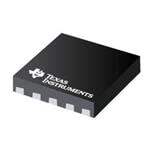
| 描述 | IC REG CTRLR BUCK PWM VM 10-SON |
| 产品分类 | |
| 品牌 | Texas Instruments |
| 数据手册 | |
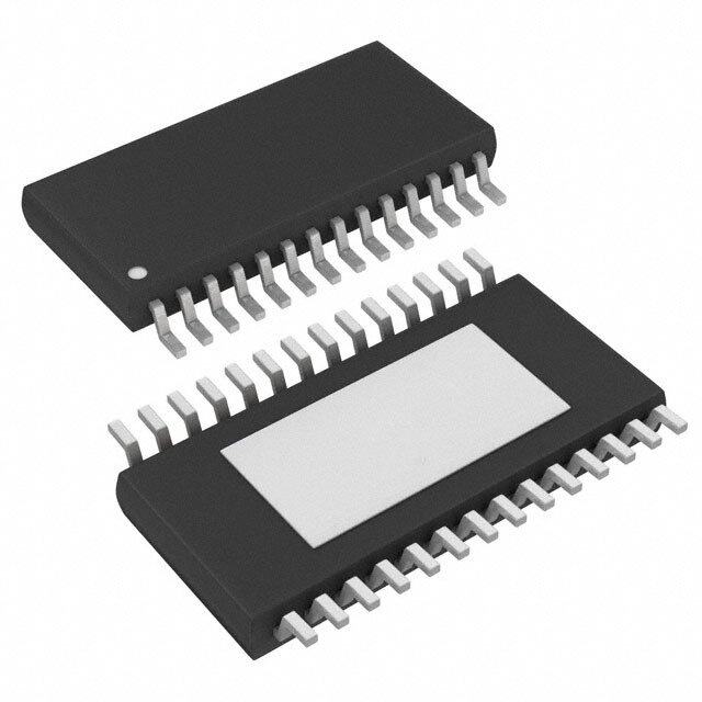
| 产品图片 |
|
| 产品型号 | TPS40304ADRCR |
| PCN设计/规格 | |
| PWM类型 | 电压模式 |
| rohs | 无铅 / 符合限制有害物质指令(RoHS)规范要求 |
| 产品系列 | - |
| 倍增器 | 无 |
| 其它名称 | 296-27478-1 |
| 分频器 | 无 |
| 包装 | 剪切带 (CT) |
| 升压 | 无 |
| 占空比 | 90% |
| 反向 | 无 |
| 反激式 | 无 |
| 封装/外壳 | 10-VFDFN 裸露焊盘 |
| 工作温度 | -40°C ~ 125°C |
| 标准包装 | 1 |
| 电压-电源 | 3 V ~ 20 V |
| 输出数 | 1 |
| 降压 | 是 |
| 隔离式 | 无 |
| 频率-最大值 | 660kHz |


PDF Datasheet 数据手册内容提取
TPS40304A www.ti.com SLUSA30 –FEBRUARY2010 3-V TO 20-V INPUT SYNCHRONOUS BUCK CONTROLLER CheckforSamples:TPS40304A FEATURES CONTENTS 1 • InputVoltageRangefrom3Vto20V DeviceRatings 2 • Fixed600-kHzSwitchingFrequency ElectricalCharacteristics 3 • High-andLow-SideFETR Current DS(on) DeviceInformation 8 Sensing ApplicationInformation 10 • ProgrammableThermallyCompensatedOCP AdditionalReferences 13 Levels • ProgrammableSoft-Start X • 591-mV,1%ReferenceVoltage APPLICATIONS • VoltageFeed-ForwardCompensation • POLModules • SupportsPre-BiasedOutput • Printer • FrequencySpreadSpectrum • DigitalTV • ThermalShutdownProtectionat145°C • Telecom • 10-Pin3mm×3mmSONPackagewith GroundConnectiontoThermalPad DESCRIPTION The TPS40304A is a cost-optimized synchronous buck controller that operates from 3-V to 20-V input. The controller implements a voltage-mode control architecture with input-voltage feed-forward compensation that respondsinstantlytoinputvoltagechange.Theswitchingfrequencyisfixedat600kHz. Frequency Spread Spectrum feature adds dither to the switching frequency, significantly reducing the peak EMI noiseandmakingitmucheasiertocomplywithEMIstandards. The TPS40304A offers design with a variety of user programmable functions, including soft-start, overcurrent protection(OCP)levels,andloopcompensation. The OCP level is programmed by a single external resistor connected from LDRV pin to circuit ground. During initial power on, the TPS40304A enters a calibration cycle, measures the voltage at the LDRV pin, and sets an internalOCPvoltagelevel.Duringoperation,theprogrammedOCPvoltageleveliscomparedtothevoltagedrop across the low-side FET when it is on to determine whether there is an overcurrent condition. The TPS40304A thenentersashutdownandrestartcycleuntilthefaultisremoved. SIMPLIFIED APPLICATION DIAGRAM V OUT TPS40304A VIN 5 FB BOOT 6 4 COMP HDRV 7 V OUT 3 PGOOD SW 8 2 EN/SS LDRV/OC 9 SD 1 VDD BP 10 V GND IN PAD UDG-10008 1 Pleasebeawarethatanimportantnoticeconcerningavailability,standardwarranty,anduseincriticalapplicationsofTexas Instrumentssemiconductorproductsanddisclaimerstheretoappearsattheendofthisdatasheet. PRODUCTIONDATAinformationiscurrentasofpublicationdate. Copyright©2010,TexasInstrumentsIncorporated Products conform to specifications per the terms of the Texas Instruments standard warranty. Production processing does not necessarilyincludetestingofallparameters.
TPS40304A SLUSA30 –FEBRUARY2010 www.ti.com This integrated circuit can be damaged by ESD. Texas Instruments recommends that all integrated circuits be handled with appropriateprecautions.Failuretoobserveproperhandlingandinstallationprocedurescancausedamage. ESDdamagecanrangefromsubtleperformancedegradationtocompletedevicefailure.Precisionintegratedcircuitsmaybemore susceptibletodamagebecauseverysmallparametricchangescouldcausethedevicenottomeetitspublishedspecifications. ORDERINGINFORMATION OPERATINGFREQUENCY PACKAGE TAPEANDREELQUANTITY PARTNUMBER 250 TPS40304ADRCT 600kHz Plastic10-PinSON(DRC) 3000 TPS40304ADRCR ABSOLUTE MAXIMUM RATINGS overoperatingfree-airtemperaturerange(unlessotherwisenoted)(1) VALUE UNIT VDD –0.3to22 V SW –3to27 V SW(<100nspulsewidth,10µJ) –5 V BOOT –0.3to30 V HDRV –5to30 V BOOT-SW,HDRV-SW(differentialfromBOOTorHDRVtoSW) –0.3to7 V COMP,PGOOD,FB,BP,LDRV,EN/SS –0.3to7 V T Operatingjunctiontemperaturerange –40to145 °C J T Storagetemperature –55to150 °C stg (1) Stressesbeyondthoselistedunderabsolutemaximumratingsmaycausepermanentdamagetothedevice.Thesearestressratings onlyandfunctionaloperationofthedeviceattheseoranyotherconditionbeyondthoseincludedunderrecommendedoperating conditionsisnotimplied.Exposuretoabsolute-maximum-ratedconditionsforextendedperiodsoftimemayaffectdevicereliability. DISSIPATION RATINGS R HIGH-KBOARD(1) POWERRATING(W) POWERRATING(W) PACKAGE AIRFLOW(LFM) qJA (°C/W) T =25°C T =85°C A A 0(NaturalConvection) 47.9 2.08 0.835 10-PinSON(DRC) 200 40.5 2.46 0.987 400 38.2 2.61 1.04 (1) RatingsbasedonJEDECHighThermalConductivity(HighK)Board.Formoreinformationonthetestmethod,seeTItechnicalbrief (SZZA017). RECOMMENDED OPERATING CONDITIONS MIN NOM MAX UNIT VDD Inputvoltage 3 20 V T Operatingjunctiontemperature –40 125 °C J ELECTROSTATIC DISCHARGE (ESD) PROTECTION MIN TYP MAX UNIT Humanbodymodel(HBM) 2000 V Chargedevicemodel(CDM) 1500 V 2 SubmitDocumentationFeedback Copyright©2010,TexasInstrumentsIncorporated ProductFolderLink(s):TPS40304A
TPS40304A www.ti.com SLUSA30 –FEBRUARY2010 ELECTRICAL CHARACTERISTICS T =–40°Cto125°C,V =12V,allparametersatzeropowerdissipation(unlessotherwisenoted) J VDD PARAMETER TESTCONDITIONS MIN TYP MAX UNIT VOLTAGEREFERENCE T =25°C,3V<V <20V 588 591 594 J VDD VFB FBinputvoltage –40°C<TJ<125°C, 585 591 597 mV 3V<V <20V VDD INPUTSUPPLY V Inputsupplyvoltagerange 3 20 V VDD IDD Shutdownsupplycurrent V <0.2V 70 100 µA SD EN/SS IDD Quiescent,non-switching LetEN/SSfloat,V =1V 2.5 3.5 mA Q FB ENABLE/SOFT-START V High-levelinputvoltage,EN/SS 0.55 0.70 1.00 V IH V Low-levelinputvoltage,EN/SS 0.27 0.30 0.33 V IL I Soft-startsourcecurrent 8 10 12 µA SS V Soft-startvoltagelevel 0.4 0.8 1.3 V SS BPREGULATOR V Outputvoltage I =10mA 6.2 6.5 6.8 V BP BP V Regulatordropoutvoltage,V –V I =25mA,V =3V 70 110 mV DO VDD BP BP VDD OSCILLATOR f PWMfrequency 3V<V <20V 540 600 660 kHz SW VDD V (1) Rampamplitude V /6.6 V /6 V /5.4 V RAMP VDD VDD VDD Frequencyspreadspectrumfrequency f 12% f SWFSS deviation SW f Modulationfrequency 25 KHz MOD PWM D (1) Maximumdutycycle V =0V,3V<V <20V 90% MAX FB VDD t (1) Minimumcontrollablepulsewidth 45 75 ns ON(min) HDRVofftoLDRVon 5 25 35 t Outputdriverdeadtime ns DEAD LDRVofftoHDRVon 5 25 30 ERRORAMPLIFIER G (1) Gainbandwidthproduct 10 24 MHz BWP A (1) Openloopgain 60 dB OL I Inputbiascurrent(currentoutofFBpin) V =0.6V 75 nA IB FB I Outputsourcecurrent V =0V 2 EAOP FB mA I Outputsinkcurrent V =1V 2 EAOM FB (1) Ensuredbydesign.Notproductiontested. Copyright©2010,TexasInstrumentsIncorporated SubmitDocumentationFeedback 3 ProductFolderLink(s):TPS40304A
TPS40304A SLUSA30 –FEBRUARY2010 www.ti.com ELECTRICAL CHARACTERISTICS (continued) T =–40°Cto125°C,V =12V,allparametersatzeropowerdissipation(unlessotherwisenoted) J VDD PARAMETER TESTCONDITIONS MIN TYP MAX UNIT PGOOD Feedbackuppervoltagelimitfor V 646 666 691 OV PGOOD Feedbacklowervoltagelimitfor mV V 491 516 541 UV PGOOD V PGOODhysteresisvoltageatFB 25 40 PGD-HYST R PGOODpulldownresistance V =0V,I =5mA 30 70 Ω PGD FB FB 541mV<V <646mV, I PGOODleakagecurrent FB 10 20 µA PGDLK V =5V PGOOD OUTPUTDRIVERS R High-sidedriverpull-upresistance V –V =5V,I =–100mA 0.8 1.5 2.5 Ω HDHI BOOT SW HDRV R High-sidedriverpull-downresistance V –V =5V,I =100mA 0.5 1.0 2.2 Ω HDLO BOOT SW HDRV R Low-sidedriverpull-upresistance I =-100mA 0.8 1.5 2.5 Ω LDHI LDRV R Low-sidedriverpull-downresistance I =100mA 0.35 0.60 1.20 Ω LDLO LDRV t (2) High-sidedriverrisetime C =5nF 15 ns HRISE LOAD t (2) High-sidedriverfalltime 12 ns HFALL t (2) Low-sidedriverrisetime 15 ns LRISE t (2) Low-sidedriverfalltime 10 ns LFALL OVERCURRENTPROTECTION t (2) Minimumpulsetimeduringshortcircuit 250 ns PSSC(min) t (2) Switchleading-edgeblankingpulsetime 150 ns BLNKH V OCthresholdforhigh-sideFET T =25°C 360 450 580 mV OCH J I OCSETcurrentsource T =25°C 9.5 10.0 10.5 µA OCSET J V MaximumclampvoltageatLDRV 260 340 400 mV LD-CLAMP OCcomparatoroffsetvoltagefor V T =25°C –8 8 mV OCLOS low-sideFET J V (2) ProgrammableOCrangeforlow-side T =25°C 12 300 mV OCLPRO FET J V (2) OCthresholdtemperaturecoefficient 3000 ppm THTC (bothhigh-sideandlow-side) t OCretrycyclesonEN/SSpin 4 Cycle OFF BOOTDIODE V Bootstrapdiodeforwardvoltage I =5mA 0.8 V DFWD BOOT THERMALSHUTDOWN T (2) Junctionshutdowntemperature 145 °C JSD T (2) Hysteresis 20 °C JSDH (2) Ensuredbydesign.Notproductiontested. 4 SubmitDocumentationFeedback Copyright©2010,TexasInstrumentsIncorporated ProductFolderLink(s):TPS40304A
TPS40304A www.ti.com SLUSA30 –FEBRUARY2010 TYPICAL CHARACTERISTICS SWITCHINGFREQUENCY QUIESCENTCURRENT vs vs JUNCTIONTEMPERATURE JUNCTIONTEMPERATURE 625 2.24 V =20V VDD 620 2.22 Hz 615 mA k – – ncy 610 rent 2.20 e r u u q 605 C Fre VVDD=12V ent 2.18 g c witchin 569050 VVDD=3V –Quies 2.16 S Q – D W 590 ID S 2.14 f 585 V =12V VDD 2.12 580 –40 –25 –10 5 20 35 50 65 80 95 110 125 –40 –25 –10 5 20 35 50 65 80 95 110 125 T –JunctionTemperature–°C T –JunctionTemperature–°C J J Figure1. Figure2. SHUTDOWNCURRENT OCSETCURRENTSOURCE vs vs JUNCTIONTEMPERATURE JUNCTIONTEMPERATURE 72 14 13 70 A A m m – – e 12 68 c nt ur urre So 11 C 66 nt wn rre do Cu 10 hut 64 ET S CS 9 –D) 62 O S – IDD( CSET 8 60 O I 7 V =12V 58 VDD 6 –40 –25 –10 5 20 35 50 65 80 95 110 125 –40 –25 –10 5 20 35 50 65 80 95 110 125 T –JunctionTemperature–°C J T –JunctionTemperature–°C J Figure3. Figure4. Copyright©2010,TexasInstrumentsIncorporated SubmitDocumentationFeedback 5 ProductFolderLink(s):TPS40304A
TPS40304A SLUSA30 –FEBRUARY2010 www.ti.com TYPICAL CHARACTERISTICS (continued) FEEDBACKREFERENCEVOLTAGE ENABLEHIGH-LEVELTHRESHOLDVOLTAGE vs vs JUNCTIONTEMPERATURE JUNCTIONTEMPERATURE 592.0 740 V m V 591.5 – m e 720 g – a age 591.0 Volt Volt 590.5 hold 700 e s c e n r e h er 590.0 T 680 ef el R v e ack 589.5 h-L b g 660 ed Hi e 589.0 e F bl – a B n 640 VF 588.5 E – H VI 588.0 620 –40 –25 –10 5 20 35 50 65 80 95 110 125 –40 –25 –10 5 20 35 50 65 80 95 110 125 TJ–JunctionTemperature–°C TJ–JunctionTemperature–°C Figure5. Figure6. ENABLELOW-LEVELTHRESHOLDVOLTAGE HIGH-SIDEOVERCURRENTTHRESHOLD vs vs JUNCTIONTEMPERATURE JUNCTIONTEMPERATURE 303.0 600 V V m m – – e302.5 d g ol 550 a h olt es V r h d302.0 T hol nt 500 s e Thre301.5 rcurr el ve ev O 450 L e Low-301.0 h-Sid e g bl Hi 400 Ena300.5 –H C – O L V VI 350 300.0 –40 –25 –10 5 20 35 50 65 80 95 110 125 –40 –25 –10 5 20 35 50 65 80 95 110 125 T –JunctionTemperature–°C T –JunctionTemperature–°C J J Figure7. Figure8. 6 SubmitDocumentationFeedback Copyright©2010,TexasInstrumentsIncorporated ProductFolderLink(s):TPS40304A
TPS40304A www.ti.com SLUSA30 –FEBRUARY2010 TYPICAL CHARACTERISTICS (continued) POWERGOODTHRESHOLDVOLTAGE SOFT-STARTVOLTAGE vs vs JUNCTIONTEMPERATURE JUNCTIONTEMPERATURE 800 1000 V m 975 – 750 Overvoltage e g a 950 olt 700 mV V – 925 d hol 650 age es olt 900 hr V T 600 rt 875 d a o St Go 550 oft- 850 er S Pow 500 –SS 825 – V V 800 U /VV 450 Undervoltage 775 O V 400 750 –40 –25 –10 5 20 35 50 65 80 95 110 125 –40 –25 –10 5 20 35 50 65 80 95 110 125 T –JunctionTemperature–°C T –JunctionTemperature–°C J J Figure9. Figure10. Copyright©2010,TexasInstrumentsIncorporated SubmitDocumentationFeedback 7 ProductFolderLink(s):TPS40304A
TPS40304A SLUSA30 –FEBRUARY2010 www.ti.com DEVICE INFORMATION TERMINAL CONFIGURATION Thepackageisan10-PinSON(DRC)package.Note:Thethermalpadisanelectricalgroundconnection. FB COMPPGOODEN/SS VDD 5 4 3 2 1 ThermalPad 6 7 8 9 10 BOOT HDRV SW LDRV/ BP OC PINFUNCTIONS TERMINAL I/O DESCRIPTION NAME NO. Gatedrivevoltageforthehigh-sideN-channelMOSFET.A100nFcapacitor(typical)mustbeconnected BOOT 6 I betweenthispinandSW.Forlowinputvoltageoperation,anexternalschottkydiodefromBPtoBOOTis recommendedtomaximizethegatedrivevoltageforthehigh-side. Outputbypassfortheinternalregulator.ConnectalowESRbypassceramiccapacitorof1µForgreaterfrom BP 10 O thispintoGND. COMP 4 O Outputoftheerroramplifierandconnectionnodeforloopfeedbackcomponents. Logiclevelinputwhichstartsorstopsthecontrollerviaanexternalusercommand.Lettingthispinfloatturns thecontrolleron.Pullingthispinlowdisablesthecontroller.Thisisalsothesoft-startprogrammingpin.A capacitorconnectedfromthispintoGNDprogramsthesoft-starttime.Thecapacitorischargedwithan internalcurrentsourceof10µA.Theresultingvoltagerampofthispinisalsousedasasecondnon-inverting EN/SS 2 I inputtotheerroramplifieraftera0.8V(typical)levelshiftdownwards.Outputregulationiscontrolledbythe internallevelshiftedvoltagerampuntilthatvoltagereachestheinternalreferencevoltageof591mV–the voltagerampofthispinreaches1.4V(typical).Optionally,a267kΩresistorfromthispintoBPenables frequencyspreadspectrumfeature. Invertinginputtotheerroramplifier.Innormaloperation,thevoltageonthispinisequaltotheinternal FB 5 I referencevoltage. PGOOD 3 O Opendrainpowergoodoutput. HDRV 7 O Bootstrappedgatedriveoutputforthehigh-sideN-channelMOSFET. Gatedriveoutputforthelow-sidesynchronousrectifierN-channelMOSFET.AresistorfromthispintoGND LDRV/OC 9 O isalsousedtodeterminethevoltagelevelforOCP.Aninternalcurrentsourceof10µAflowsthroughthe resistorduringinitialcalibrationandthatsetsupthevoltagetrippointusedforOCP. Powerinputtothecontroller.BypassVDDtoGNDwithalowESRceramiccapacitorofatleast1.0-µFclose VDD 1 I tothedevice. Senselinefortheadaptiveanti-crossconductioncircuitry.Servesascommonconnectionfortheflying SW 8 O high-sideFETdriver. Groundconnectiontothecontroller.Thisisalsothethermalpadusedtoconductheatfromthedevice.This Thermal connectionservesatwofoldpurpose.Thefirstistoprovideanelectricalgroundconnectionforthedevice. GND Pad ThesecondistoprovidealowthermalimpedancepathfromthedevicedietothePCB.Thispadshouldbe tiedexternallytoagroundplane. 8 SubmitDocumentationFeedback Copyright©2010,TexasInstrumentsIncorporated ProductFolderLink(s):TPS40304A
TPS40304A www.ti.com SLUSA30 –FEBRUARY2010 TPS40304A BLOCK DIAGRAM + 0.591V +12.5% 10mA REF SoftStart SS SS FB BP EN/SS 2 + SD Clock Fault 0.591VREF–12.5% 6 BOOT Controller VDD 1 6-V + OC 7 HDRV Regulator References 0.591V REF SD BP 10 BP 8 SW COMP 4 CaCliibrcrautiiton SSppercetraudm Clock Anti-Cross BP Conduction Oscillator PWM and Logic Pre-Bias 9 LDRV/OC FB 5 Circuit PWM + + 0.591V 10mA REF SS 750kW SThhuetdrmowaln ThrOesChold PGOOD 3 Setting FaultController OC PAD UDG-01009 GND Copyright©2010,TexasInstrumentsIncorporated SubmitDocumentationFeedback 9 ProductFolderLink(s):TPS40304A
TPS40304A SLUSA30 –FEBRUARY2010 www.ti.com APPLICATION INFORMATION Introduction The TPS40304A is a cost-optimized synchronous buck controller providing high-end features to construct high-performance DC/DC converters. Pre-bias capability eliminates concerns about damaging sensitive loads during startup. Programmable overcurrent protection levels and hiccup overcurrent fault recovery maximize design flexibility and minimize power dissipation in the event of a prolonged output short. Frequency Spread Spectrum (FSS) feature reduces peak EMI noise by spreading the initial energy of each harmonic along a frequencyband,thusgivingawiderspectrumwithloweramplitudes. Voltage Reference The 591-mV band gap cell is internally connected to the non-inverting input of the error amplifier. The reference voltage is trimmed with the error amplifier in a unity gain configuration to remove amplifier offset from the final regulation voltage. The 1% tolerance on the reference voltage allows the user to design a very accurate power supply. Enable Functionality, Startup Sequence and Timing After input power is applied, an internal current source of 40 µA starts to charge up the soft-start capacitor connectedfromEN/SStoGND.Whenthevoltageacrossthatcapacitorincreasesto0.7V,itenablestheinternal BP regulator followed by a calibration. The total calibration time is about 1.9 ms. See Figure 11. During the calibration, the device performs in the following way. It disables the LDRV drive and injects an internal 10 µA current source to the resistor connected from LDRV to GND. The voltage developed across that resistor is then sampledandlatchedinternallyastheOCPtripleveluntilonecyclestheinputortogglestheEN/SS. 2.0 V EN/SS Calibration 1.6 Time V 1.9ms – e ag 1.3V olt 1.2 V ut p n –I 0.8 N 0.7V VI 0.4 V SS_INT 0 t–Time–ms UDG-09159 Figure11. StartupSequenceandTiming The voltage at EN/SS is internally clamped to 1.3 V before and/or during calibration to minimize the discharging time once calibration is complete. The discharging current is from an internal current source of 140 µA and it pulls the voltage down to 0.4 V. It then initiates the soft-start by charging up the capacitor using an internal current source of 10 µA. The resulting voltage ramp on this pin is used as a second non-inverting input to the error amplifier after an 800 mV (typical) downward level-shift; therefore, actual soft-start will not take place until thevoltageatthispinreaches800mV. If EN/SS is left floating, the controller starts automatically. EN/SS must be pulled down to less than 270 mV to guaranteethatthechipisinshutdownmode. 10 SubmitDocumentationFeedback Copyright©2010,TexasInstrumentsIncorporated ProductFolderLink(s):TPS40304A
TPS40304A www.ti.com SLUSA30 –FEBRUARY2010 Soft-Start Time The soft-start time of the TPS40304A is user programmable by selecting a single capacitor. The EN/SS pin sources 10 µA to charge this capacitor. The actual output ramp-up time is the amount of time that it takes for the 10 µA to charge the capacitor through a 591-mV range. There is some initial lag due to calibration and an offset (800mV)fromtheactualEN/SSpinvoltagetothevoltageappliedtotheerroramplifier. The soft-start is done in a closed loop fashion, meaning that the error amplifier controls the output voltage at all times during the soft start period and the feedback loop is never open as occurs in duty cycle limit soft-start schemes. The error amplifier has two non-inverting inputs, one connected to the 591-mV reference voltage, and the other connected to the offset EN/SS pin voltage. The lower of these two voltages is what the error amplifier controls the FB pin to. As the voltage on the EN/SS pin ramps up past approximately 1.4 V (800 mV offset voltage plus the 591-mV reference voltage), the 591-mV reference voltage becomes the dominant input and the converterhasreacheditsfinalregulationvoltage. Thecapacitorrequiredforagivensoft-startramptimefortheoutputvoltageisgivenbyEquation1. CSS =æçVISS ö÷´tSS è FB ø where • C istherequiredcapacitanceontheEN/SSpin(F) SS • I isthesoft-startsourcecurrent(10µA) SS • V isthefeedbackreferencevoltage(591mV) FB • t isthedesiredsoft-startramptime(s) (1) SS Oscillator and Frequency Spread Spectrum (FSS) Theoscillatorfrequencyisinternallyfixedat600kHz. Connecting a resistor with a value of 267 kΩ ±10% from BP to EN/SS enables the FSS feature. When enabled, it spreads the internal oscillator frequency over a minimum 12% window using a 25-kHz modulation frequency with triangular profile. By modulating the switching frequency, side-bands are created. The emission power of the fundamental switching frequency and its harmonics is distributed into smaller pieces scattered around many side-band frequencies. The effect significantly reduces the peak EMI noise and makes it much easier for the resultantemissionspectrumtopassEMIregulations. Overcurrent Protection Programmable OCP level at LDRV is from 6 mV to 150 mV at room temperature with 3000 ppm temperature coefficient to help compensate for changes in the low-side FET channel resistance as temperature increases. With a scale factor of 2, the actual trip point across the low-side FET is in the range of 12 mV to 300 mV. The accuracy of the internal current source is ±5%. Overall offset voltage, including the offset voltage of the internal comparatorandtheamplifierforscalefactorof2,islimitedto±8mV. Maximum clamp voltage at LDRV is 340 mV to avoid turning on the low-side FET during calibration and in a pre-biased condition. The maximum clamp voltage is fixed and it does not change with temperature. If the voltage drop across R reaches the 340 mV maximum clamp voltage during calibration (No R resistor OCSET OCSET included),itdisablesOCP.Oncedisabled,thereisnolow-sideorhigh-sidecurrentsensing. OCP level at HDRV is fixed at 450 mV with 3000 ppm temperature coefficient to help compensate for changes in the high-side FET channel resistance as temperature increases. OCP at HDRV provides pulse-by-pulse current limiting. Copyright©2010,TexasInstrumentsIncorporated SubmitDocumentationFeedback 11 ProductFolderLink(s):TPS40304A
TPS40304A SLUSA30 –FEBRUARY2010 www.ti.com OCPsensingatLDRVisatrueinductorvalleycurrentdetection,usingsampleandhold.Equation2canbeused tocalculateR : OCSET æçæçIOUT(max)-æçIP2-P ÷öö÷´RDS(on)-VOCLOS ö÷ ROCSET = ççè è 2 ´øIOøCSET ÷÷ ç ÷ ç ÷ è ø where • I istheinternalcurrentsource OCSET • V istheoveralloffsetvoltage OCLOS • I isthepeak-to-peakinductorcurrent P-P • R isthedraintosourceon-resistanceofthelow-sideFET DS(on) • I isthetrippointforOCP OUT(max) • R istheresistorusedforsettingtheOCPlevel (2) OCSET Toavoidovercurrenttrippinginnormaloperatingloadrange,calculateR usingtheequationabovewith: OCSET • ThemaximumR atroomtemperature DS(ON) • The lower limit of V (–8 mV) and the lower limit of I (9.5 µA) from the Electrical Characteristics OCLOS OCSET table. • Thepeak-to-peakinductorcurrentI atminimuminputvoltage P-P Overcurrentissensedacrossboththelow-sideFETandthehigh-sideFET.IfthevoltagedropacrosseitherFET exceeds the OC threshold, a count increments one count. If no OC is detected on either FET, the fault counter decrements by one count. If three OC pulses are summed, a fault condition is declared which cycles the soft-start function in a hiccup mode. Hiccup mode consists of four dummy soft-start timeouts followed by a real one if overcurrent condition is encountered during normal operation, or five dummy soft-start timeouts followed byarealoneifovercurrentconditionoccursfromthebeginningduringstart.Thiscyclecontinuesindefinitelyuntil thefaultconditionisremoved. Drivers The drivers for the external high-side and low-side MOSFETs are capable of driving a gate-to-source voltage of V . The LDRV driver for the low-side MOSFET switches between BP and GND, while HDRV driver for the BP high-side MOSFET is referenced to SW and switches between BOOT and SW. The drivers have non-overlapping timing that is governed by an adaptive delay circuit to minimize body diode conduction in the synchronousrectifier. Pre-Bias Startup The TPS40304A contains a circuit to prevent current from being pulled from the output during startup in the condition the output is pre-biased. There are no PWM pulses until the internal soft-start voltage rises above the error amplifier input (FB pin), if the output is pre-biased. Once the soft-start voltage exceeds the error amplifier input, the controller slowly initiates synchronous rectification by starting the synchronous rectifier with a narrow ontime.Itthenincrementsthatontimeonacycle-by-cyclebasisuntilitcoincideswiththetimedictatedby(1-D), where D is the duty cycle of the converter. This approach prevents the sinking of current from a pre-biased output,andensurestheoutputvoltagestartupandramptoregulationissmoothandcontrolled. 12 SubmitDocumentationFeedback Copyright©2010,TexasInstrumentsIncorporated ProductFolderLink(s):TPS40304A
TPS40304A www.ti.com SLUSA30 –FEBRUARY2010 Power Good The TPS40304A provides an indication that output is good for the converter. This is an open drain signal and pulls low when any condition exists that would indicate that the output of the supply might be out of regulation. Theseconditionsincludethefollowing: • V ismorethan±12.5%fromnominal FB • Soft-startisactive • Ashortcircuitconditionhasbeendetected NOTE When there is no power to the device, PGOOD is not able to pull close to GND if an auxiliary supply is used for the power good indication. In this case, a built in resistor connected from drain to gate on the PGOOD pull down device makes the PGOOD pin lookapproximatelylikeadiodetoGND. Thermal Shutdown Ifthejunctiontemperatureofthedevicereachesthethermalshutdownlimitof145°C,thePWMandtheoscillator are turned off and HDRV and LDRV are driven low. When the junction cools to the required level (125°C typical), thePWMinitiatessoftstartasduringanormalpower-upcycle. ADDITIONAL REFERENCES Related Devices ThedeviceslistedinhavecharacteristicssimilartotheTPS40304Aandmaybeofinterest. Table1.RelatedDevices DEVICE DESCRIPTION TPS40303/4/5 3-Vto20-VInputSynchronousBuckController References These references, design tools and links to additional references, including design software, may be found at http://power.ti.com 1. AdditionalPowerPAD™informationmaybefoundinApplicationsBriefs(SLMA002A)and(SLMA004). 2. UnderTheHoodOfLowVoltageDC/DCConverters–SEM1500Topic5– 2002SeminarSeries 3. UnderstandingBuckPowerStagesinSwitchmodePowerSupplies,(SLVA057),March1999 4. DesigningStableControlLoops–SEM1400– 2001SeminarSeries Package Outline and Recommended PCB Footprint The following pages outline the mechanical dimensions of the 10-pin DRC package and provide recommendationsforPCBlayout. Copyright©2010,TexasInstrumentsIncorporated SubmitDocumentationFeedback 13 ProductFolderLink(s):TPS40304A
PACKAGE OPTION ADDENDUM www.ti.com 6-Feb-2020 PACKAGING INFORMATION Orderable Device Status Package Type Package Pins Package Eco Plan Lead/Ball Finish MSL Peak Temp Op Temp (°C) Device Marking Samples (1) Drawing Qty (2) (6) (3) (4/5) TPS40304ADRCR ACTIVE VSON DRC 10 3000 Green (RoHS NIPDAUAG Level-2-260C-1 YEAR -40 to 145 304A & no Sb/Br) TPS40304ADRCT ACTIVE VSON DRC 10 250 Green (RoHS NIPDAUAG Level-2-260C-1 YEAR -40 to 145 304A & no Sb/Br) (1) The marketing status values are defined as follows: ACTIVE: Product device recommended for new designs. LIFEBUY: TI has announced that the device will be discontinued, and a lifetime-buy period is in effect. NRND: Not recommended for new designs. Device is in production to support existing customers, but TI does not recommend using this part in a new design. PREVIEW: Device has been announced but is not in production. Samples may or may not be available. OBSOLETE: TI has discontinued the production of the device. (2) RoHS: TI defines "RoHS" to mean semiconductor products that are compliant with the current EU RoHS requirements for all 10 RoHS substances, including the requirement that RoHS substance do not exceed 0.1% by weight in homogeneous materials. Where designed to be soldered at high temperatures, "RoHS" products are suitable for use in specified lead-free processes. TI may reference these types of products as "Pb-Free". RoHS Exempt: TI defines "RoHS Exempt" to mean products that contain lead but are compliant with EU RoHS pursuant to a specific EU RoHS exemption. Green: TI defines "Green" to mean the content of Chlorine (Cl) and Bromine (Br) based flame retardants meet JS709B low halogen requirements of <=1000ppm threshold. Antimony trioxide based flame retardants must also meet the <=1000ppm threshold requirement. (3) MSL, Peak Temp. - The Moisture Sensitivity Level rating according to the JEDEC industry standard classifications, and peak solder temperature. (4) There may be additional marking, which relates to the logo, the lot trace code information, or the environmental category on the device. (5) Multiple Device Markings will be inside parentheses. Only one Device Marking contained in parentheses and separated by a "~" will appear on a device. If a line is indented then it is a continuation of the previous line and the two combined represent the entire Device Marking for that device. (6) Lead/Ball Finish - Orderable Devices may have multiple material finish options. Finish options are separated by a vertical ruled line. Lead/Ball Finish values may wrap to two lines if the finish value exceeds the maximum column width. Important Information and Disclaimer:The information provided on this page represents TI's knowledge and belief as of the date that it is provided. TI bases its knowledge and belief on information provided by third parties, and makes no representation or warranty as to the accuracy of such information. Efforts are underway to better integrate information from third parties. TI has taken and continues to take reasonable steps to provide representative and accurate information but may not have conducted destructive testing or chemical analysis on incoming materials and chemicals. TI and TI suppliers consider certain information to be proprietary, and thus CAS numbers and other limited information may not be available for release. In no event shall TI's liability arising out of such information exceed the total purchase price of the TI part(s) at issue in this document sold by TI to Customer on an annual basis. Addendum-Page 1
PACKAGE OPTION ADDENDUM www.ti.com 6-Feb-2020 Addendum-Page 2
PACKAGE MATERIALS INFORMATION www.ti.com 20-Jul-2019 TAPE AND REEL INFORMATION *Alldimensionsarenominal Device Package Package Pins SPQ Reel Reel A0 B0 K0 P1 W Pin1 Type Drawing Diameter Width (mm) (mm) (mm) (mm) (mm) Quadrant (mm) W1(mm) TPS40304ADRCR VSON DRC 10 3000 330.0 12.4 3.3 3.3 1.1 8.0 12.0 Q2 TPS40304ADRCT VSON DRC 10 250 180.0 12.4 3.3 3.3 1.1 8.0 12.0 Q2 PackMaterials-Page1
PACKAGE MATERIALS INFORMATION www.ti.com 20-Jul-2019 *Alldimensionsarenominal Device PackageType PackageDrawing Pins SPQ Length(mm) Width(mm) Height(mm) TPS40304ADRCR VSON DRC 10 3000 367.0 367.0 35.0 TPS40304ADRCT VSON DRC 10 250 210.0 185.0 35.0 PackMaterials-Page2
GENERIC PACKAGE VIEW DRC 10 VSON - 1 mm max height PLASTIC SMALL OUTLINE - NO LEAD Images above are just a representation of the package family, actual package may vary. Refer to the product data sheet for package details. 4204102-3/M
IMPORTANTNOTICEANDDISCLAIMER TI PROVIDES TECHNICAL AND RELIABILITY DATA (INCLUDING DATASHEETS), DESIGN RESOURCES (INCLUDING REFERENCE DESIGNS), APPLICATION OR OTHER DESIGN ADVICE, WEB TOOLS, SAFETY INFORMATION, AND OTHER RESOURCES “AS IS” AND WITH ALL FAULTS, AND DISCLAIMS ALL WARRANTIES, EXPRESS AND IMPLIED, INCLUDING WITHOUT LIMITATION ANY IMPLIED WARRANTIES OF MERCHANTABILITY, FITNESS FOR A PARTICULAR PURPOSE OR NON-INFRINGEMENT OF THIRD PARTY INTELLECTUAL PROPERTY RIGHTS. These resources are intended for skilled developers designing with TI products. You are solely responsible for (1) selecting the appropriate TI products for your application, (2) designing, validating and testing your application, and (3) ensuring your application meets applicable standards, and any other safety, security, or other requirements. These resources are subject to change without notice. TI grants you permission to use these resources only for development of an application that uses the TI products described in the resource. Other reproduction and display of these resources is prohibited. No license is granted to any other TI intellectual property right or to any third party intellectual property right. TI disclaims responsibility for, and you will fully indemnify TI and its representatives against, any claims, damages, costs, losses, and liabilities arising out of your use of these resources. TI’s products are provided subject to TI’s Terms of Sale (www.ti.com/legal/termsofsale.html) or other applicable terms available either on ti.com or provided in conjunction with such TI products. TI’s provision of these resources does not expand or otherwise alter TI’s applicable warranties or warranty disclaimers for TI products. Mailing Address: Texas Instruments, Post Office Box 655303, Dallas, Texas 75265 Copyright © 2020, Texas Instruments Incorporated