ICGOO在线商城 > 集成电路(IC) > PMIC - 稳压器 - DC DC 切换控制器 > UC2525BN

 Datasheet下载
- 型号: UC2525BN
- 制造商: Texas Instruments
- 库位|库存: xxxx|xxxx
- 要求:
| 数量阶梯 | 香港交货 | 国内含税 |
| +xxxx | $xxxx | ¥xxxx |
查看当月历史价格
查看今年历史价格
UC2525BN产品简介:
ICGOO电子元器件商城为您提供UC2525BN由Texas Instruments设计生产,在icgoo商城现货销售,并且可以通过原厂、代理商等渠道进行代购。 UC2525BN价格参考¥21.29-¥39.55。Texas InstrumentsUC2525BN封装/规格:PMIC - 稳压器 - DC DC 切换控制器, 升压,反激,正激转换器,全桥,半桥,推挽 稳压器 正 输出 升压,升压/降压 DC-DC 控制器 IC 16-PDIP。您可以下载UC2525BN参考资料、Datasheet数据手册功能说明书,资料中有UC2525BN 详细功能的应用电路图电压和使用方法及教程。
UC2525BN 是 Texas Instruments(德州仪器)生产的一款高性能、双端 PWM 控制器,常用于开关电源设计中。该芯片具有高精度误差放大器、可调频率振荡器、软启动功能和过流保护等特性,广泛应用于需要高效能和稳定输出的 DC-DC 转换场景。

典型应用场景包括:

1. 工业电源系统:如PLC电源模块、工控设备供电系统,提供稳定的电压转换。
2. 通信设备电源:用于电信基站、网络交换设备中的DC-DC电源模块。
3. 电动汽车充电设备:在车载充电机或充电桩内部作为主控PWM芯片。
4. 太阳能逆变器:用于将太阳能板输出的直流电升压后供给逆变系统。
5. 电机驱动电源:为伺服电机、步进电机等提供高效稳定的驱动电压。
6. 实验室电源与测试设备:构建可调输出的高精度电源供应装置。

UC2525BN 支持多种拓扑结构,如推挽式、半桥、全桥等,适用于中高功率的开关电源设计,尤其适合对效率、稳定性和可靠性有较高要求的应用场合。
| 参数 | 数值 |
| 产品目录 | 集成电路 (IC)半导体 |
| Cuk | 无 |
| 描述 | IC REG CTRLR BST FLYBK VM 16DIP开关控制器 Regulating Pulse Width Modulator |
| 产品分类 | |
| 品牌 | Texas Instruments |
| 产品手册 | |
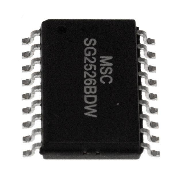
| 产品图片 |
|
| rohs | 符合RoHS无铅 / 符合限制有害物质指令(RoHS)规范要求 |
| 产品系列 | 电源管理 IC,开关控制器 ,Texas Instruments UC2525BN- |
| 数据手册 | |
| 产品型号 | UC2525BN |
| PWM类型 | 电压模式 |
| 上升时间 | 100 ns |
| 下降时间 | 50 ns |
| 产品种类 | 开关控制器 |
| 倍增器 | 无 |
| 其它名称 | 296-34703-5 |
| 分频器 | 无 |
| 包装 | 管件 |
| 升压 | 是 |
| 单位重量 | 1.054 g |
| 占空比 | 50% |
| 占空比-最大 | 50 % |
| 反向 | 无 |
| 反激式 | 是 |
| 同步管脚 | Yes |
| 商标 | Texas Instruments |
| 安装风格 | Through Hole |
| 封装 | Tube |
| 封装/外壳 | 16-DIP(0.300",7.62mm) |
| 封装/箱体 | PDIP-16 |
| 工作温度 | -40°C ~ 85°C |
| 工厂包装数量 | 25 |
| 开关频率 | 450 kHz |
| 拓扑结构 | Boost, Flyback, Forward, Full-Bridge, Half-Bridge, Push-Pull |
| 最大工作温度 | + 85 C |
| 最小工作温度 | - 25 C |
| 标准包装 | 25 |
| 电压-电源 | 8 V ~ 35 V |
| 类型 | Voltage Mode PWM Controllers |
| 系列 | UC2525A |
| 输出数 | 2 |
| 输出电流 | 400 mA |
| 输出端数量 | 2 Output |
| 降压 | 无 |
| 隔离式 | 无 |
| 频率-最大值 | 400kHz |


- 商务部:美国ITC正式对集成电路等产品启动337调查
- 曝三星4nm工艺存在良率问题 高通将骁龙8 Gen1或转产台积电
- 太阳诱电将投资9.5亿元在常州建新厂生产MLCC 预计2023年完工
- 英特尔发布欧洲新工厂建设计划 深化IDM 2.0 战略
- 台积电先进制程称霸业界 有大客户加持明年业绩稳了
- 达到5530亿美元!SIA预计今年全球半导体销售额将创下新高
- 英特尔拟将自动驾驶子公司Mobileye上市 估值或超500亿美元
- 三星加码芯片和SET,合并消费电子和移动部门,撤换高东真等 CEO
- 三星电子宣布重大人事变动 还合并消费电子和移动部门
- 海关总署:前11个月进口集成电路产品价值2.52万亿元 增长14.8%


PDF Datasheet 数据手册内容提取
UC3527B Not Recommended For New Designs application UC1525B UC1527B INFO UC2525B UC2527B available UC3525B UC3527B Regulating Pulse Width Modulators FEATURES DESCRIPTION • 8to35VOperation The UC1525B/1527B series of pulse width modulator integrated circuits are designed to offer improved performance and lowered external parts • 5.1VBuriedZenerReference count when used in designing all types of switching power supplies. The Trimmedto±0.75% on-chip +5.1V buried zener reference is trimmed to ±0.75% and the input • 100Hzto500kHzOscillatorRange common-mode range of the error amplifier includes the reference voltage, eliminating external resistors. A sync input to the oscillator allows multiple • SeparateOscillatorSyncTerminal units to be slaved or a single unit to be synchronized to an external system • AdjustableDeadtimeControl clock.AsingleresistorbetweentheCTandthedischargeterminalsprovide a wide range of dead time adjustment. These devices also feature built-in • InternalSoft-Start soft-start circuitry with only an external timing capacitor required. A shut- • Pulse-by-PulseShutdown down terminal controls both the soft-start circuitry and the output stages, providing instantaneous turn off through the PWM latch with pulsed shut- • InputUndervoltageLockoutwith down, as well as soft-start recycle with longer shutdown commands. These Hysteresis functions are also controlled by an undervoltage lockout which keeps the • LatchingPWMtoPreventMultiple outputsoffandthesoft-startcapacitordischargedforsub-normalinputvolt- Pulses ages. This lockout circuitry includes approximately 500mV of hysteresis for jitter-freeoperation.AnotherfeatureofthesePWMcircuitsisalatchfollow- • DualSource/SinkOutputDrivers ing the comparator. Once a PWM pulse has been terminated for any rea- • LowCrossConductionOutputStage son, the outputs will remain off for the duration of the period. The latch is reset with each clock pulse. The output stages are totem-pole designs ca- • TighterReferenceSpecifications pable of sourcing or sinking in excess of 200mA. The UC1525B output stage features NOR logic, giving a LOW output for an OFF state. The UC1527ButilizesORlogicwhichresultsinaHIGHoutputlevelwhenOFF. BLOCK DIAGRAM UDG-95055 SLUS376JULY1995
UC3527B Not Recommended For New Designs UC1525B UC1527B UC2525B UC2527B UC3525B UC3527B ABSOLUTE MAXIMUM RATINGS RECOMMENDED OPERATING CONDITIONS (Note 1) SupplyVoltage,(+VIN) ...........................+40V CollectorSupplyVoltage(VC)......................+40V InputVoltage(+VIN) .......................+8Vto+35V LogicInputs ............................–0.3Vto+5.5V CollectorSupplyVoltage(VC) ..............+4.5Vto+35V AnalogInputs.............................–0.3VtoVIN Sink/SourceLoadCurrent(steadystate) ........0to100mA OutputCurrent,SourceorSink ...................500mA Sink/SourceLoadCurrent(peak) ..............0to400mA ReferenceOutputCurrent ........................50mA ReferenceLoadCurrent ......................0to20mA OscillatorChargingCurrent ........................5mA OscillatorFrequencyRange..............100Hzto400kHz PowerDissipationatTA=+25°C.................1000mW OscillatorTimingResistor ..................2kΩto150kΩ PowerDissipationatTC=+25°C ................2000mW OscillatorTimingCapacitor ..............0.001µFto0.1µF OperatingJunctionTemperature ..........–55°Cto+150°C DeadTimeResistorRange...................0Ωto500Ω StorageTemperatureRange .............–65°Cto+150°C Note1:Rangeoverwhichthedeviceisfunctionalandparame- LeadTemperature(Soldering,10sec.).............+300°C terlimitsareguaranteed. All currents are positive into, negative out of the specified ter- minal.ConsultPackagingSectionofDatabookforthermallimi- tationsandconsiderationsofpackages. CONNECTION DIAGRAMS DIL-16,SOIC-16(TopView) LCC-20,PLCC-20(TopView) JorN,DWPackages L,QPackages ELECTRICAL CHARACTERISTICS:Unlessotherwisestated,thesespecificationsapplyforT =–55°Cto+125°Cforthe A UC1525BandUC1527B;–40°Cto+85°CfortheUC2525BandUC2527B;0°Cto+70°CfortheUC3525BandUC3527B;+VIN= 20V,T =T . A J UC1525B/UC2525B UC3525B UC1527B/UC2527B UC3527B PARAMETER TESTCONDITIONS MIN TYP MAX MIN TYP MAX UNITS ReferenceSection OutputVoltage T =25°C 5.062 5.10 5.138 5.036 5.10 5.164 V J LineRegulation VIN=8Vto35V 5 10 5 10 mV LoadRegulation I =0mAto20mA 7 15 7 15 mV L TemperatureStability(Note2) OverOperatingRange 10 50 10 50 mV TotalOutputVariation Line,Load,andTemperature 5.036 5.164 5.024 5.176 V ShortCircuitCurrent VREF=0,T =25°C 80 100 80 100 mA J OutputNoiseVoltage(Note2) 10Hz≤f≤10kHz,TJ=25°C 40 200 40 200 µVrms LongTermStability(Note2) T =125°C,1000Hrs. 3 10 3 10 mV J 2
UC3527B Not Recommended For New Designs UC1525B UC1527B UC2525B UC2527B UC3525B UC3527B ELECTRICAL CHARACTERISTICS:Unlessotherwisestated,thesespecificationsapplyforT =–55°Cto+125°Cforthe A UC1525BandUC1527B;–40°Cto+85°CfortheUC2525BandUC2527B;0°Cto+70°CfortheUC3525BandUC3527B;+VIN= 20V,T =T . A J UC1525B/UC2525B UC3525B UC1527B/UC2527B UC3527B PARAMETER TESTCONDITIONS MIN TYP MAX MIN TYP MAX UNITS OscillatorSection(Note3) InitialAccuracy(Notes2&3) T =25°C ±2 ±6 ±2 ±6 % J VoltageStability(Notes2&3) VIN=8Vto35V ±0.3 ±1 ±1 ±2 % TemperatureStability(Note2) OverOperatingRange ±3 ±6 ±3 ±6 % MinimumFrequency RT=200k(cid:1),CT=0.1(cid:2)F 120 120 Hz MaximumFrequency RT=2k(cid:1),CT=470pF 400 400 kHz CurrentMirror I =2mA 1.7 2.0 2.2 1.7 2.0 2.2 mA RT ClockAmplitude(Notes2&3) 3.0 3.5 3.0 3.5 V ClockWidth(Notes2&3) T =25°C 0.3 0.5 1.0 0.3 0.5 1.0 (cid:2)s J SyncThreshold 1.2 2.0 2.8 1.2 2.0 2.8 V SyncInputCurrent SyncVoltage=3.5V 1.0 2.5 1.0 2.5 mA ErrorAmplifierSection(VCM=5.1V) InputOffsetVoltage 0.5 5 2 10 mV InputBiasCurrent 1 10 1 10 (cid:2)A InputOffsetCurrent 1 1 (cid:2)A DCOpenLoopGain RL(cid:3)10Meg(cid:1) 60 75 60 75 dB Gain-BandwidthProduct(Note2) A =0dB,T =25°C 1 2 1 2 MHz V J OutputLowLevel 0.2 0.5 0.2 0.5 V OutputHighLevel 3.8 5.6 3.8 5.6 V CommonModeRejection V =1.5Vto5.2V 60 75 60 75 dB CM SupplyVoltageRejection VIN=8Vto35V 50 60 50 60 dB PWMComparator MinimumDutyCycle 0 0 % MaximumDutyCycle(Note3) 45 49 45 49 % InputThreshold(Note3) ZeroDutyCycle 0.7 0.9 0.7 0.9 V InputThreshold(Note3) MaximumDutyCycle 3.3 3.6 3.3 3.6 V InputBiasCurrent(Note2) 0.05 1.0 0.05 1.0 (cid:2)A ShutdownSection SoftStartCurrent V =0V,V 25 50 80 25 50 80 (cid:2)A SHUTDOWN SOFTSTART =0V SoftStartLowLevel V =2.5V 0.4 0.7 0.4 0.7 V SHUTDOWN ShutdownThreshold Tooutputs,V = 0.6 0.8 1.0 0.6 0.8 1.0 V SOFTSTART 5.1V,T =25°C J ShutdownInputCurrent V =2.5V 0.4 1.0 0.4 1.0 mA SHUTDOWN ShutdownDelay(Note2) V =2.5V,T =25°C 0.2 0.5 0.2 0.5 (cid:2)s SHUTDOWN J OutputDrivers(EachOutput)(Vc=20V) OutputLowLevel I =20mA 0.2 0.4 0.2 0.4 V SINK I =100mA 1.0 2.0 1.0 2.0 V SINK OutputHIghLevel I =20mA 18 19 18 19 V SOURCE I =100mA 17 18 17 18 V SOURCE UndervoltageLockout V andV = 6 7 8 6 7 8 V COMP SOFTSTART High CollectorLeakage VC=35V 200 200 (cid:2)A 3
UC3527B Not Recommended For New Designs UC1525B UC1527B UC2525B UC2527B UC3525B UC3527B ELECTRICAL CHARACTERISTICS:Unlessotherwisestated,thesespecificationsapplyforT =–55°Cto+125°Cforthe A UC1525BandUC1527B;–40°Cto+85°CfortheUC2525BandUC2527B;0°Cto+70°CfortheUC3525BandUC3527B;+VIN= 20V,T =T . A J UC1525B/UC2525B UC3525B UC1527B/UC2527B UC3527B PARAMETER TESTCONDITIONS MIN TYP MAX MIN TYP MAX UNITS OutputDrivers(EachOutput)(VC=20V)(cont.) RiseTime(Note2) C =1nF,T =25°C 100 600 100 600 ns L J FallTime(Note2) C =1nF,T =25°C 50 300 50 300 ns L J Crossconductioncharge Percycle,T =25°C 30 30 nc J TotalStandbyCurrent SupplyCurrent VIN=35V 14 20 14 20 mA Note2:Ensuredbydesign.Not100%testedinproduction. Note3:Testedatfosc=40kHz(RT=3.6K(cid:1),CT=0.01(cid:2)F,RD=0(cid:1)).Approximateoscillatorfrequencyisdefinedby: 1 f = CT •(0.7•RT +3RD) PRINCIPLES OF OPERATION AND TYPICAL CHARACTERISTICS UC1525BOutputCircuit(1/2CircuitShown) UC1525BOutputSaturationCharacteristics UDG-95056 UDG-95057 UDG-95059 UDG-95058 In conventional push-pull bipolar designs, forward base For single-ended supplies, the driver outputs are drive is controlled by R1-R3. Rapid turn-off times for the grounded.TheVCterminalisswitchedtogroundbytheto- power devices are achieved with speed-up capacitors C, tem-polesourcetransistorsonalternateoscillatorcycles. andC2. 4
UC3527B Not Recommended For New Designs UC1525B UC1527B UC2525B UC2527B UC3525B UC3527B UDG-95060 UDG-95061 The low source impedance of the output drivers provides Low power transformers can be driven directly by the rapid charging of power FETinput capacitance while mini- UC1525B. Automatic reset occurs during dead time, when mizingexternalcomponents. bothendsoftheprimarywindingareswitchedtoground. PRINCIPLES OF OPERATION AND TYPICAL CHARACTERISTICS ShutdownOptions(SeeBlockDiagram) plyingapositivesignalonPin10performstwofunctions: the PWM latch is immediately set providing the fastest Since both the compensation and soft-start terminals turn-off signal to the external soft-start capacitor. If the (Pins 9 and 8) have current source pull-ups, either can shutdown command is short, the PWM signal is termi- readilyacceptapull-downsignalwhichonlyhastosinka nated without significant discharge of the soft-start ca- maximumof100µAtoturnofftheoutputs.Thisissubject pacitor, thus, allowing, for example, a convenient to the added requirement of discharging whatever exter- implementation of pulse-by-pulse current limiting. nalcapacitancemaybeattachedtothesepins. Holding Pin 10 high for a longer duration, however, will An alternate approach is the use of the shutdown cir- ultimately discharge this external capacitor, recycling cuitryofPin10whichhasbeenimprovedtoenhancethe slowturn-onuponrelease. available shutdown options. Activating this circuit by ap- UC1525BOscillatorSchematic UDG-95062 5
UC3527B Not Recommended For New Designs UC1525B UC1527B UC2525B UC2527B UC3525B UC3527B OscillatorChargeTimevs.RandC OscillatorDischargeTimevs.RandC T T D T UDG-95063 UDG-95064 UC1525BErrorAmplifier ErrorAmplifierOpen-LoopFrequencyResponse UDG-95065 UDG-95066 6
UC3527B Not Recommended For New Designs UC1525B UC1527B UC2525B UC2527B UC3525B UC3527B LABTESTFIXTURE UDG-95067 7
PACKAGE OPTION ADDENDUM www.ti.com 6-Feb-2020 PACKAGING INFORMATION Orderable Device Status Package Type Package Pins Package Eco Plan Lead/Ball Finish MSL Peak Temp Op Temp (°C) Device Marking Samples (1) Drawing Qty (2) (6) (3) (4/5) 5962-8951105EA ACTIVE CDIP J 16 1 TBD Call TI N / A for Pkg Type -55 to 125 5962-8951105EA UC1525BJ/883B UC1525BJ ACTIVE CDIP J 16 1 TBD Call TI N / A for Pkg Type -55 to 125 UC1525BJ UC1525BJ883B ACTIVE CDIP J 16 1 TBD Call TI N / A for Pkg Type -55 to 125 5962-8951105EA UC1525BJ/883B UC2525BDWTR ACTIVE SOIC DW 16 2000 Green (RoHS NIPDAU Level-2-260C-1 YEAR -40 to 85 UC2525BDW & no Sb/Br) UC3525BDW ACTIVE SOIC DW 16 40 Green (RoHS NIPDAU Level-2-260C-1 YEAR 0 to 70 UC3525BDW & no Sb/Br) UC3525BDWG4 ACTIVE SOIC DW 16 40 Green (RoHS NIPDAU Level-2-260C-1 YEAR 0 to 70 UC3525BDW & no Sb/Br) UC3525BDWTR ACTIVE SOIC DW 16 2000 Green (RoHS NIPDAU Level-2-260C-1 YEAR 0 to 70 UC3525BDW & no Sb/Br) UC3525BN ACTIVE PDIP N 16 25 Green (RoHS NIPDAU N / A for Pkg Type 0 to 70 UC3525BN & no Sb/Br) (1) The marketing status values are defined as follows: ACTIVE: Product device recommended for new designs. LIFEBUY: TI has announced that the device will be discontinued, and a lifetime-buy period is in effect. NRND: Not recommended for new designs. Device is in production to support existing customers, but TI does not recommend using this part in a new design. PREVIEW: Device has been announced but is not in production. Samples may or may not be available. OBSOLETE: TI has discontinued the production of the device. (2) RoHS: TI defines "RoHS" to mean semiconductor products that are compliant with the current EU RoHS requirements for all 10 RoHS substances, including the requirement that RoHS substance do not exceed 0.1% by weight in homogeneous materials. Where designed to be soldered at high temperatures, "RoHS" products are suitable for use in specified lead-free processes. TI may reference these types of products as "Pb-Free". RoHS Exempt: TI defines "RoHS Exempt" to mean products that contain lead but are compliant with EU RoHS pursuant to a specific EU RoHS exemption. Green: TI defines "Green" to mean the content of Chlorine (Cl) and Bromine (Br) based flame retardants meet JS709B low halogen requirements of <=1000ppm threshold. Antimony trioxide based flame retardants must also meet the <=1000ppm threshold requirement. (3) MSL, Peak Temp. - The Moisture Sensitivity Level rating according to the JEDEC industry standard classifications, and peak solder temperature. (4) There may be additional marking, which relates to the logo, the lot trace code information, or the environmental category on the device. Addendum-Page 1
PACKAGE OPTION ADDENDUM www.ti.com 6-Feb-2020 (5) Multiple Device Markings will be inside parentheses. Only one Device Marking contained in parentheses and separated by a "~" will appear on a device. If a line is indented then it is a continuation of the previous line and the two combined represent the entire Device Marking for that device. (6) Lead/Ball Finish - Orderable Devices may have multiple material finish options. Finish options are separated by a vertical ruled line. Lead/Ball Finish values may wrap to two lines if the finish value exceeds the maximum column width. Important Information and Disclaimer:The information provided on this page represents TI's knowledge and belief as of the date that it is provided. TI bases its knowledge and belief on information provided by third parties, and makes no representation or warranty as to the accuracy of such information. Efforts are underway to better integrate information from third parties. TI has taken and continues to take reasonable steps to provide representative and accurate information but may not have conducted destructive testing or chemical analysis on incoming materials and chemicals. TI and TI suppliers consider certain information to be proprietary, and thus CAS numbers and other limited information may not be available for release. In no event shall TI's liability arising out of such information exceed the total purchase price of the TI part(s) at issue in this document sold by TI to Customer on an annual basis. OTHER QUALIFIED VERSIONS OF UC1525B, UC3525B : •Catalog: UC3525B •Military: UC1525B •Space: UC1525B-SP NOTE: Qualified Version Definitions: •Catalog - TI's standard catalog product •Military - QML certified for Military and Defense Applications •Space - Radiation tolerant, ceramic packaging and qualified for use in Space-based application Addendum-Page 2
PACKAGE MATERIALS INFORMATION www.ti.com 26-Mar-2013 TAPE AND REEL INFORMATION *Alldimensionsarenominal Device Package Package Pins SPQ Reel Reel A0 B0 K0 P1 W Pin1 Type Drawing Diameter Width (mm) (mm) (mm) (mm) (mm) Quadrant (mm) W1(mm) UC2525BDWTR SOIC DW 16 2000 330.0 16.4 10.75 10.7 2.7 12.0 16.0 Q1 PackMaterials-Page1
PACKAGE MATERIALS INFORMATION www.ti.com 26-Mar-2013 *Alldimensionsarenominal Device PackageType PackageDrawing Pins SPQ Length(mm) Width(mm) Height(mm) UC2525BDWTR SOIC DW 16 2000 367.0 367.0 38.0 PackMaterials-Page2
GENERIC PACKAGE VIEW DW 16 SOIC - 2.65 mm max height 7.5 x 10.3, 1.27 mm pitch SMALL OUTLINE INTEGRATED CIRCUIT This image is a representation of the package family, actual package may vary. Refer to the product data sheet for package details. 4224780/A www.ti.com
PACKAGE OUTLINE DW0016A SOIC - 2.65 mm max height SCALE 1.500 SOIC C 10.63 SEATING PLANE TYP 9.97 A PIN 1 ID 0.1 C AREA 14X 1.27 16 1 10.5 2X 10.1 8.89 NOTE 3 8 9 0.51 16X 0.31 7.6 B 7.4 0.25 C A B 2.65 MAX NOTE 4 0.33 TYP 0.10 SEE DETAIL A 0.25 GAGE PLANE 0.3 0 - 8 0.1 1.27 0.40 DETAIL A (1.4) TYPICAL 4220721/A 07/2016 NOTES: 1. All linear dimensions are in millimeters. Dimensions in parenthesis are for reference only. Dimensioning and tolerancing per ASME Y14.5M. 2. This drawing is subject to change without notice. 3. This dimension does not include mold flash, protrusions, or gate burrs. Mold flash, protrusions, or gate burrs shall not exceed 0.15 mm, per side. 4. This dimension does not include interlead flash. Interlead flash shall not exceed 0.25 mm, per side. 5. Reference JEDEC registration MS-013. www.ti.com
EXAMPLE BOARD LAYOUT DW0016A SOIC - 2.65 mm max height SOIC 16X (2) SEE SYMM DETAILS 1 16 16X (0.6) SYMM 14X (1.27) 8 9 R0.05 TYP (9.3) LAND PATTERN EXAMPLE SCALE:7X METAL SOLDER MASK SOLDER MASK METAL OPENING OPENING 0.07 MAX 0.07 MIN ALL AROUND ALL AROUND NON SOLDER MASK SOLDER MASK DEFINED DEFINED SOLDER MASK DETAILS 4220721/A 07/2016 NOTES: (continued) 6. Publication IPC-7351 may have alternate designs. 7. Solder mask tolerances between and around signal pads can vary based on board fabrication site. www.ti.com
EXAMPLE STENCIL DESIGN DW0016A SOIC - 2.65 mm max height SOIC 16X (2) SYMM 1 16 16X (0.6) SYMM 14X (1.27) 8 9 R0.05 TYP (9.3) SOLDER PASTE EXAMPLE BASED ON 0.125 mm THICK STENCIL SCALE:7X 4220721/A 07/2016 NOTES: (continued) 8. Laser cutting apertures with trapezoidal walls and rounded corners may offer better paste release. IPC-7525 may have alternate design recommendations. 9. Board assembly site may have different recommendations for stencil design. www.ti.com
None
None
IMPORTANTNOTICEANDDISCLAIMER TI PROVIDES TECHNICAL AND RELIABILITY DATA (INCLUDING DATASHEETS), DESIGN RESOURCES (INCLUDING REFERENCE DESIGNS), APPLICATION OR OTHER DESIGN ADVICE, WEB TOOLS, SAFETY INFORMATION, AND OTHER RESOURCES “AS IS” AND WITH ALL FAULTS, AND DISCLAIMS ALL WARRANTIES, EXPRESS AND IMPLIED, INCLUDING WITHOUT LIMITATION ANY IMPLIED WARRANTIES OF MERCHANTABILITY, FITNESS FOR A PARTICULAR PURPOSE OR NON-INFRINGEMENT OF THIRD PARTY INTELLECTUAL PROPERTY RIGHTS. These resources are intended for skilled developers designing with TI products. You are solely responsible for (1) selecting the appropriate TI products for your application, (2) designing, validating and testing your application, and (3) ensuring your application meets applicable standards, and any other safety, security, or other requirements. These resources are subject to change without notice. TI grants you permission to use these resources only for development of an application that uses the TI products described in the resource. Other reproduction and display of these resources is prohibited. No license is granted to any other TI intellectual property right or to any third party intellectual property right. TI disclaims responsibility for, and you will fully indemnify TI and its representatives against, any claims, damages, costs, losses, and liabilities arising out of your use of these resources. TI’s products are provided subject to TI’s Terms of Sale (www.ti.com/legal/termsofsale.html) or other applicable terms available either on ti.com or provided in conjunction with such TI products. TI’s provision of these resources does not expand or otherwise alter TI’s applicable warranties or warranty disclaimers for TI products. Mailing Address: Texas Instruments, Post Office Box 655303, Dallas, Texas 75265 Copyright © 2020, Texas Instruments Incorporated