ICGOO在线商城 > 集成电路(IC) > PMIC - 稳压器 - DC DC 切换控制器 > TPS51124RGER
 Datasheet下载
- 型号: TPS51124RGER
- 制造商: Texas Instruments
- 库位|库存: xxxx|xxxx
- 要求:
| 数量阶梯 | 香港交货 | 国内含税 |
| +xxxx | $xxxx | ¥xxxx |
查看当月历史价格
查看今年历史价格
TPS51124RGER产品简介:
ICGOO电子元器件商城为您提供TPS51124RGER由Texas Instruments设计生产,在icgoo商城现货销售,并且可以通过原厂、代理商等渠道进行代购。 TPS51124RGER价格参考¥10.28-¥10.28。Texas InstrumentsTPS51124RGER封装/规格:PMIC - 稳压器 - DC DC 切换控制器, 降压 稳压器 正 输出 降压 DC-DC 控制器 IC 24-VQFN(4x4)。您可以下载TPS51124RGER参考资料、Datasheet数据手册功能说明书,资料中有TPS51124RGER 详细功能的应用电路图电压和使用方法及教程。
TPS51124RGER是德州仪器(Texas Instruments)生产的一款PMIC(电源管理集成电路),具体分类为DC-DC切换控制器。它主要应用于需要高效、紧凑和高性能电源解决方案的场景中,尤其适用于便携式电子设备和对电源效率要求较高的系统。

 应用场景

1. 便携式电子产品:
   - TPS51124RGER非常适合用于智能手机、平板电脑、笔记本电脑等便携式设备。这些设备通常需要高效的电源管理来延长电池寿命,并且要求小型化设计以适应紧凑的空间。

2. 通信设备:
   - 在基站、路由器和其他通信基础设施中,TPS51124RGER可以提供稳定的电源输出,确保信号传输的可靠性和稳定性。其高效的电源转换能力有助于减少功耗和热量产生。

3. 工业控制系统:
   - 工业自动化和控制系统中,TPS51124RGER能够为微控制器、传感器和其他关键组件提供稳定的电源支持。其宽输入电压范围和高效率特性使其在工业环境中表现出色。

4. 医疗设备:
   - 医疗设备如监护仪、便携式诊断设备等,对电源的稳定性和可靠性要求极高。TPS51124RGER能够提供精确的电压调节,确保设备在各种工作条件下都能正常运行。

5. 消费类电子产品:
   - 例如智能手表、可穿戴设备等,TPS51124RGER的小尺寸和低功耗特性使得它成为这些设备的理想选择。它可以帮助设计人员在有限的空间内实现高效的电源管理。

6. 汽车电子:
   - 在汽车电子系统中,如信息娱乐系统、导航系统和高级驾驶辅助系统(ADAS),TPS51124RGER可以提供稳定的电源供应,确保系统的可靠性和安全性。

 特点与优势

- 高效率:通过优化的开关频率和控制算法,TPS51124RGER能够在不同负载条件下保持高效率,减少能量损耗。
- 小尺寸:采用紧凑的封装设计,适合空间受限的应用场景。
- 宽输入电压范围:支持较宽的输入电压范围,适应多种电源输入条件。
- 集成保护功能:内置过流、过温、短路等保护机制,提高系统的安全性和可靠性。

综上所述,TPS51124RGER凭借其高效、紧凑和可靠的性能,广泛应用于各类需要高性能电源管理的场景中。
| 参数 | 数值 |
| 产品目录 | 集成电路 (IC)半导体 |
| Cuk | 无 |
| 描述 | IC REG CTRLR BUCK PWM 24-QFN开关控制器 Dual Sync Step Down for Lo-Vltg Sys Pwr |
| DevelopmentKit | TPS51124EVM-001 |
| 产品分类 | |
| 品牌 | Texas Instruments |
| 产品手册 | http://www.ti.com/litv/slvs616b |
| 产品图片 |
|
| rohs | 符合RoHS无铅 / 符合限制有害物质指令(RoHS)规范要求 |
| 产品系列 | 电源管理 IC,开关控制器 ,Texas Instruments TPS51124RGERD-CAP™ |
| 数据手册 | |
| 产品型号 | TPS51124RGER |
| PWM类型 | 混合物 |
| 产品种类 | 开关控制器 |
| 倍增器 | 无 |
| 其它名称 | 296-26976-6 |
| 分频器 | 无 |
| 包装 | Digi-Reel® |
| 升压 | 无 |
| 单位重量 | 45.400 mg |
| 占空比 | 88% |
| 反向 | 无 |
| 反激式 | 无 |
| 商标 | Texas Instruments |
| 安装风格 | SMD/SMT |
| 封装 | Reel |
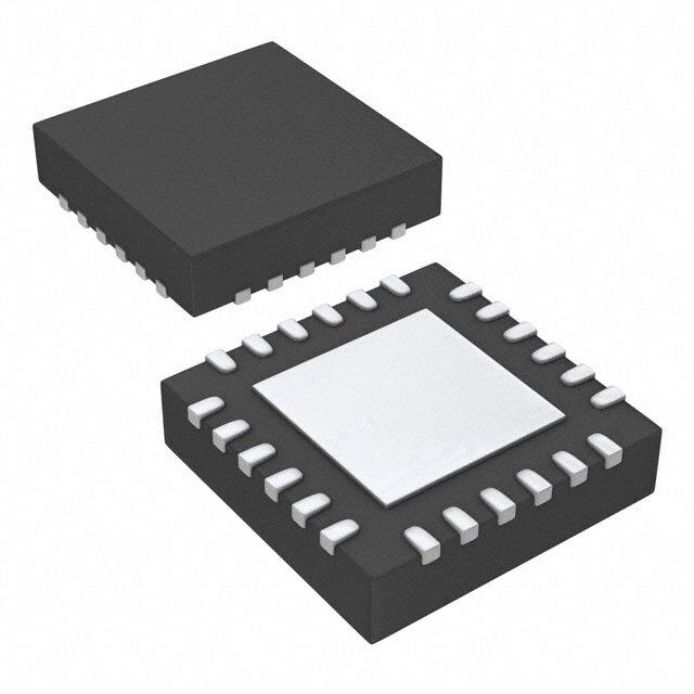
| 封装/外壳 | 24-VFQFN 裸露焊盘 |
| 封装/箱体 | VQFN-24 |
| 工作温度 | -40°C ~ 85°C |
| 工厂包装数量 | 3000 |
| 最大工作温度 | + 85 C |
| 最小工作温度 | - 40 C |
| 标准包装 | 1 |
| 电压-电源 | 4.5 V ~ 5.5 V |
| 类型 | DC/DC Controller (External Switch) |
| 系列 | TPS51124 |
| 输入电压 | 3 V to 28 V |
| 输出数 | 2 |
| 输出电压 | 0.75 V to 5.5 V |
| 输出电流 | 15 A |
| 输出端数量 | 2 Output |
| 配用 | /product-detail/zh/TPS51124EVM-001/296-31420-ND/1671774 |
| 降压 | 是 |
| 隔离式 | 无 |
| 频率-最大值 | 420kHz |


- 商务部:美国ITC正式对集成电路等产品启动337调查
- 曝三星4nm工艺存在良率问题 高通将骁龙8 Gen1或转产台积电
- 太阳诱电将投资9.5亿元在常州建新厂生产MLCC 预计2023年完工
- 英特尔发布欧洲新工厂建设计划 深化IDM 2.0 战略
- 台积电先进制程称霸业界 有大客户加持明年业绩稳了
- 达到5530亿美元!SIA预计今年全球半导体销售额将创下新高
- 英特尔拟将自动驾驶子公司Mobileye上市 估值或超500亿美元
- 三星加码芯片和SET,合并消费电子和移动部门,撤换高东真等 CEO
- 三星电子宣布重大人事变动 还合并消费电子和移动部门
- 海关总署:前11个月进口集成电路产品价值2.52万亿元 增长14.8%


PDF Datasheet 数据手册内容提取
Product Sample & Technical Tools & Support & Folder Buy Documents Software Community TPS51124 SLVS616C–NOVEMBER2005–REVISEDDECEMBER2014 TPS51124 Dual Synchronous Step-Down Controller for Low-Voltage Power Rails 1 Features 3 Description • HighEfficiency,Low-PowerConsumption, The TPS51124 is a dual, adaptive on-time D-CAP™ 1 mode synchronous buck controller. The part enables Shutdownsto <1 μA system designers to cost effectively complete the • FixedFrequencyEmulatedOn-TimeControl, suite of notebook power bus regulators with the FrequencySelectableFromThreeOptions absolute lowest external component count and lowest • D-CAP™ModeEnablesFastTransientResponse standby consumption. The fixed frequency emulated adaptive on-time control supports seamless operation • Auto-SkipMode between PWM mode at heavy load condition and • LessThan1%InitialReferenceAccuracy reduced frequency operation at light load for high • LowOutputRipple efficiency down to milliampere range. The main • WideInputVoltageRange:3Vto28V control loop for the TPS51124 uses the D-CAP mode that optimized for low ESR output capacitors such as • OutputVoltageRange:0.76Vto5.5V POSCAP or SP-CAP promises fast transient • Low-SideRDS(ON)Loss-lessCurrentSensing response with no external compensation. Simple and • AdaptiveGateDriversWithIntegratedBoost separate power good signals for each channel allow Diode flexibility of power sequencing. The part provides a convenient and efficient operation with supply input • Internal1.2-msVoltage-ServoSoft-Start voltages (V5IN, V5FILT) ranging from 4.5 V to 5.5 V, • PowergoodSignalsforEachChannelWithDelay conversion voltages (drain voltage for the Timer synchronous high-side MOSFET) from 3 V to 28 V • OutputDischargeDuringDisable,Fault andoutputvoltagesfrom0.76Vto5.5V. The TPS51124 is available in 24-pin VQFN package 2 Applications specified from –40°C to 85°C ambient temperature NotebookI/OandLow-VoltageSystemBus range. DeviceInformation(1) PARTNUMBER PACKAGE BODYSIZE(NOM) TPS51124 VQFN(24) 4.00mm×4.00mm (1) For all available packages, see the orderable addendum at theendofthedatasheet. Input Voltage 3 V to 28 V 2C2 9µF 73.2R k4Ω75 RkΩ5 SGND kR7Ω52 28.R7 1kΩ 6 5 4 3 2 1 SGNDPGND PGoowode2r 7 PGOOVO2D2 VFB2 TONSEL GND VFB1 PVO1GOOD124 PGoowode1r EN2 8 EN2 EN123 EN1 1.V5O V2/10A 10 Cµ6F 1IR LµF2QH73821 0.1C µ5F 190VDBRSVTH22 TPS(Q51F1N2244R)GE DVBRSVTH1122120.C1 2µF IRFQ71821 1 Lµ1HC310 µF VO1 Q4 11LL2 LL120 Q2 1.05 V/10A 2 x 330C µ4F IRF8113 12DRVL2PGND2 TRIP2 V5FILT V5IN TRIP1 PGND1DRVL119 IRF8113 2C x1 330 µF 13 14 15 16 17 18 R7 R3 V5IN PGND 6.8 kΩR6 3.3Ω 6k.Ω8 PGND 4.5 V to 5.5 V C7 C8 4.7μF 1μF PGND SGND 1 An IMPORTANT NOTICE at the end of this data sheet addresses availability, warranty, changes, use in safety-critical applications, intellectualpropertymattersandotherimportantdisclaimers.PRODUCTIONDATA.
TPS51124 SLVS616C–NOVEMBER2005–REVISEDDECEMBER2014 www.ti.com Table of Contents 1 Features.................................................................. 1 7.4 DeviceFunctionalModes........................................13 2 Applications........................................................... 1 8 ApplicationandImplementation........................ 14 3 Description............................................................. 1 8.1 ApplicationInformation............................................14 4 RevisionHistory..................................................... 2 8.2 TypicalApplication..................................................14 5 PinConfigurationandFunctions......................... 3 9 PowerSupplyRecommendations...................... 18 6 Specifications......................................................... 4 10 Layout................................................................... 18 6.1 AbsoluteMaximumRatings ....................................4 10.1 LayoutGuidelines.................................................18 6.2 RecommendedOperatingConditions......................4 10.2 LayoutExample....................................................19 6.3 ThermalInformation..................................................4 11 DeviceandDocumentationSupport................. 20 6.4 ElectricalCharacteristics..........................................5 11.1 Third-PartyProductsDisclaimer...........................20 6.5 TypicalCharacteristics..............................................7 11.2 Trademarks...........................................................20 7 DetailedDescription............................................ 10 11.3 ElectrostaticDischargeCaution............................20 7.1 Overview.................................................................10 11.4 Glossary................................................................20 7.2 FunctionalBlockDiagram.......................................10 12 Mechanical,Packaging,andOrderable Information........................................................... 20 7.3 FeatureDescription.................................................11 4 Revision History ChangesfromRevisionB(September2010)toRevisionC Page • AddedESDRatingstable,FeatureDescriptionsection,DeviceFunctionalModes,ApplicationandImplementation section,PowerSupplyRecommendationssection,Layoutsection,DeviceandDocumentationSupportsection,and Mechanical,Packaging,andOrderableInformationsection.................................................................................................. 1 ChangesfromRevisionA(November2005)toRevisionB Page • ChangedFrom:pin48=PGND1To:pin18=PGND1inthePinOutillustration................................................................. 3 • UpdatedtheFunctionBlockDiagram................................................................................................................................... 10 • Figure19-RemovedthehystereticsymbolfromthePWMcomponent.............................................................................. 15 • Updatedequation9.ChangedFrom:V x0.01To:V x0.0132.................................................................................. 16 OUT OUT ChangesfromOriginal(November2005)toRevisionA Page • Updatedthethecircutillustration,Pin21changedFromDRVL1To:DRVH1andPin19changedFrom:DRVH1to DRVL1.................................................................................................................................................................................... 1 • PGlowhysteresis(PGOODxgoeslow)-deletedtheMin-4%andMax-6%values........................................................... 6 • PGhighhysteresis(PGOODxgoeslow)-deletedtheMin4%andMax6%values............................................................ 6 • Hysteresis(recovery<20μs)-deletedtheMin8%andMax12%values........................................................................... 6 • UpdatedFigure18,Pin21changedFromDRVL1To:DRVH1andPin19changedFrom:DRVH1toDRVL1................. 14 2 SubmitDocumentationFeedback Copyright©2005–2014,TexasInstrumentsIncorporated ProductFolderLinks:TPS51124
TPS51124 www.ti.com SLVS616C–NOVEMBER2005–REVISEDDECEMBER2014 5 Pin Configuration and Functions RGEPackage 24-PinVQFNWithExposedThermalPad TopView 1 PGOOD EN1 VBST1 DRVH1 LL1 DRVL1 4 3 2 1 0 9 2 2 2 2 2 1 VO1 1 18 PGND1 VFB1 2 17 TRIP1 GND 3 16 V5IN Thermal Pad TONSEL 4 15 V5FILT VFB2 5 14 TRIP2 VO2 6 13 PGND2 7 8 9 01 11 21 2 2 2 2 2 2 D N T H L L O E S V L V OG BV RD RD P PinFunctions PIN I/O DESCRIPTION NAME NO. DRVH1 21 Synchronoushigh-sideMOSFETdriveroutputs.LLnodereferencedfloatingdrivers.Thegatedrivevoltage O DRVH2 10 isdefinedbythevoltageacrossVBSTtoLLnodeflyingcapacitor. DRVL1 19 Synchronouslow-sideMOSFETdriveroutputs.PGNDreferenceddrivers.Thegate-drivevoltageisdefined O DRVL2 12 byV5INvoltage. EN1 23 I Channel1andchannel2enablepins.Connectto5Vor3.3VtoturnonSMPS EN2 8 GND 3 I Signalgroundpin LL1 20 Switchnodeconnectionsforhigh-sidedriversreturn.Alsoserveasinputtocurrentcomparatorsandinput I/O LL2 11 voltagemonitorforon-timecontrolcircuitry. PGND1 18 GroundreturnsforDRVL1andDRVL2.Alsoserveasinputofcurrentcomparators.ConnectPGND1, I/O PGND2 13 PGND2,andGNDstronglytogetherneartheIC.Outputdischargecurrentflowsthroughthispin,also. PGOOD1 24 PowerGoodwindowcomparatoropendrainoutputforchannel1and2.Pullupwitharesistorto5V,or O appropriatesignalvoltage.Currentcapabilityis5mA.PGOODgoeshigh0.5msafterVFBcomeswithin PGOOD2 7 specifiedlimits.Powerbad,ortheterminalgoeslow,iswithin10μs. TONSEL 4 I On-timeselectionpin.SeeTable1. TRIP1 17 Overcurrenttrippointsetinput.ConnectresistorfromthispintoGNDtosetthresholdforsynchronouslow- I sideR sense.VoltageacrossthispinandGNDiscomparedtovoltageacrossPGNDandLLatover- DS(on) TRIP2 14 currentcomparator. VBST1 22 Supplyinputforsynchronoushigh-sideMOSFETdriver(BoostTerminal).Connectcapacitorfromthispin I torespectiveLLterminals.AninternalPNdiodeisconnectedbetweenV5INtoeachofthesepins.User VBST2 9 canaddexternalSchottkydiodeifforwarddropiscriticaltodrivetheMOSFET. VFB1 2 I SMPSvoltagefeedbackinputs.Connectwithfeedbackresistordivider. VFB2 5 VO1 1 OutputconnectionstoSMPS.Theseterminalsservetwofunctions:On-timeadjustmentandoutput I VO2 6 discharge. 5-VpowersupplyinputfortheentirecontrolcircuitexcepttheMOSFETdrivers.ConnectRClow-passfilter V5FILT 15 I fromV5INtoV5FILT. V5IN 16 I 5-VpowersupplyinputforFETgatedrivers.InternallyconnectedtoVBSTxbyPNdiodes. Copyright©2005–2014,TexasInstrumentsIncorporated SubmitDocumentationFeedback 3 ProductFolderLinks:TPS51124
TPS51124 SLVS616C–NOVEMBER2005–REVISEDDECEMBER2014 www.ti.com 6 Specifications 6.1 Absolute Maximum Ratings(1) overoperatingfree-airtemperaturerange(unlessotherwisenoted) MIN MAX UNIT VBST1,VBST2 –0.3 36 VBST1,VBST2(wrtLLx) –0.3 6 Inputvoltage V V5IN,V5FILT,EN1,EN2,VFB1,VFB2,TRIP1,TRIP2,VO1, –0.3 6 VO2,TONSEL DRVH1,DRVH2 –1 36 DRVH1,DRVH2(wrtLLx) –0.3 6 Output LL1,LL2 –2 30 V voltage PGOOD1,PGOOD2,DRVL1,DRVL2 –0.3 6 PGND1,PGND2 –0.3 0.3 T Operatingambienttemperature –40 85 °C A T Junctiontemperature –40 125 °C J T Storagetemperature –55 150 °C stg (1) Stressesbeyondthoselistedunderabsolutemaximumratingsmaycausepermanentdamagetothedevice.Thesearestressratings onlyandfunctionaloperationofthedeviceattheseoranyotherconditionsbeyondthoseindicatedunderrecommendedoperating conditionsisnotimplied.Exposuretoabsolute-maximum-ratedconditionsforextendedperiodsmayaffectdevicereliability.Allvoltage valuesarewithrespecttothenetworkgroundterminalunlessotherwisenoted 6.2 Recommended Operating Conditions overoperatingfree-airtemperature(unlessotherwisenoted) MIN MAX UNIT Supplyinputvoltage V5IN,V5FILT 4.5 5.5 V VBST1,VBST2 –0.1 34 Inputvoltage VBST1,VBST2(wrtLLx) –0.1 5.5 V EN1,EN2,VFB1,VFB2,TRIP1,TRIP2,VO1,VO2,TONSEL –0.1 5.5 DRVH1,DRVH2 –0.8 34 DRVH1,DRVH2(wrtLLx) –0.1 5.5 Outputvoltage LL1,LL2 –1.8 28 V PGOOD1,PGOOD2,DRVL1,DRVL2 –0.1 5.5 PGND1,PGND2 –0.1 0.1 T Operatingambienttemperature –40 85 °C A 6.3 Thermal Information TPS51124 THERMALMETRIC(1) VQFN UNIT 24PINS R Junction-to-ambientthermalresistance 42.9 °C/W θJA (1) Formoreinformationabouttraditionalandnewthermalmetrics,seetheICPackageThermalMetricsapplicationreport,SPRA953. 4 SubmitDocumentationFeedback Copyright©2005–2014,TexasInstrumentsIncorporated ProductFolderLinks:TPS51124
TPS51124 www.ti.com SLVS616C–NOVEMBER2005–REVISEDDECEMBER2014 6.4 Electrical Characteristics overoperatingfree-airtemperaturerange,V5IN=V5FILT=5V(unlessotherwisenoted) PARAMETER TESTCONDITIONS MIN TYP MAX UNIT SUPPLYCURRENT V5FILTcurrent,noload, I V5FILTsupplycurrent EN1=EN2=5V,VFB1=VFB2=0.77V, 350 700 μA V5FILT LL1=LL2=0.5V I V5INshutdowncurrent V5INcurrent,noload,EN1=EN2=0V 1 μA V5INSDN I V5FILTshutdowncurrent V5FILTcurrent,noload,EN1=EN2=0V 1 μA V5FILTSD N VFBVOLTAGEandDISCHARGERESISTANCE V VFBregulationvoltage FBvoltage,skipmode(f /10) 764 mV VFB PWM T =25°C,bandgapinitialaccuracy –0.9% 0.9% A V VFBregulationvoltage T =0°Cto85°C(1) –1.3% 1.3% VFB tolerance A T =–40°Cto85°C(1) –1.6% 1.6% A VFBregulationshiftin 0.758-Vtargetforresistordivider.SeePWMOperationof VVFBSKIP continuousconduction DetailedDescription(1) 758 mV I VFBinputcurrent VFBx=0.758V,absolutevalue 0.02 0.1 μA VFB R VOdischargeresistance ENx=0V,VOx=0.5V,T =25°C 10 20 Ω Dischg A OUTPUT:N-CHANEELMOSFETGATEDRIVERS Source,V =0.5V 5 7 Ω VBSTx–DRVHx R DRVHresistance DRVH Sink,V =0.5V 1.5 2.5 Ω DRVHx-LLx Source,V =0.5V 4 6 Ω V5IN–DRVLx R DRVLresistance DRVL Sink,V =0.5V 1 2.0 Ω DRVLx–PGNDx DRVHx-low(DRVHx=1V)toDRVLx-on 10 20 50 ns (DRVLx=4V),LL=–0.05V, T Deadtime D DRVLx-low(DRVLx=1V)toDRVHx-on 30 40 60 ns (DRVHx=4V),LL=–0.05V, INTERNALBSTDIODE V Forwardvoltage V ,I =10mA,T =25°C 0.7 0.8 0.9 V FBST V5IN–VBSTx F A VBST=34V,LL=28V,VOx=5.5V, I VBSTleakagecurrent 0.1 1 μA VBSTLK T =25°C A ON-TIMETIMERCONTROLANDINTERNALSOFTSTART, T CH1,240-kHzsetting VO1=1.5V,TONSEL=GND,LL1=12V 440 500 560 ns ON11 T CH1,300-kHzsetting VO1=1.5V,TONSEL=FLOAT,LL1=12V 340 390 440 ns ON12 T CH1,360-kHzsetting VO1=1.5V,TONSEL=V5FILT,LL1=12V 265 305 345 ns ON13 T CH2,300-kHzsetting VO2=1.05V,TONSEL=GND,LL2=12V 235 270 305 ns ON21 T CH2,360-kHzsetting VO2=1.05V,TONSEL=FLOAT,LL2=12V 180 210 240 ns ON22 T CH2,420-kHzsetting VO2=1.05V,TONSEL=V5FILT,LL2=12V 120 150 180 ns ON23 T CH2Ontime VO2=0.76V,TONSEL=V5FILT,LL2=28V 80 110 140 ns ON(MIN) T CH1/CH2Min.offtime LL=–0.1V,T =25°C,VFB=0.7V 435 ns OFF(MIN) A Internalsoftstart,timefromENx>3VtoVFBxregulationvalue= T InternalSStime 0.85 1.2 1.40 ms ss 735mV UVLO/LOGICTHRESHOLD Wakeup 3.7 4.0 4.3 V V5FILTUVLOthreshold V UV5VFILT Hysteresis 0.2 0.3 0.4 Wakeup 1.0 1.3 1.5 V ENxthreshold V EN Hysteresis 0.2 I ENxinputcurrent Absolutevalue(2) 0.02 0.1 μA EN (1) Specifiedbydesign.Notproductiontested. (2) Ensuredbydesign.Notproductiontested. Copyright©2005–2014,TexasInstrumentsIncorporated SubmitDocumentationFeedback 5 ProductFolderLinks:TPS51124
TPS51124 SLVS616C–NOVEMBER2005–REVISEDDECEMBER2014 www.ti.com Electrical Characteristics (continued) overoperatingfree-airtemperaturerange,V5IN=V5FILT=5V(unlessotherwisenoted) PARAMETER TESTCONDITIONS MIN TYP MAX UNIT Fast(2) V5FIL T–0.3 V TONSELthreshold Medium(2) V5FILT V TONSEL 2 –1.0 Slow(2) 0.5 TONSEL=0V,currentoutofthepin(2) 1 I TONSELinputcurrent μA TONSEL TONSEL=5V,currentintothepin(2) 1 CURRENTSENSE I TRIPsourcecurrent VTRIPx<0.3V,T =25°C 9 10 11 μA TRIP A I temperature Onthebasisof25°C(2) ppm/° TC TRIP 4200 ITRIP coeffficent C (V –V )voltage, V OCPcompensationoffset TRIPx-GND PGNDx-LLx –10 0 10 mV OCLoff V =60mV TRIPx-GND Zerocrossdetection VPGNDx-LLxvoltage,PGOODx=Hi(2) V 0.5 mV ZC comparatoroffset Currentlimitthreshold V voltage,alltemperatures(2) V TRIPx-GND 30 200 mV Rtrip settingrange POWERGOODCOMPARATOR PGinfromlower(PGOODxgoeshi) 92.5% 95% 97.5% PGlowhysteresis(PGOODxgoeslow) –5% VTHPG PGthreshold PGinfromhigher(PGOODxgoeshi) 102.5 105% 107.5% % PGhighhysteresis(PGOODxgoeslow) 5% I PGsinkcurrent PGOODx=0.5V 2.5 5.0 mA PGMAX T PGdelay DelayforPGin 400 510 620 μs PGDEL OUTPUTUNDERVOLTAGEANDOVERVOLTAGEPROTECTION V OutputOVPtripthreshold OVPdetect 110% 115% 120% OVP t OutputOVPpropdelay 1.5 μs OVPDEL V OutputUVPtripthreshold Hysteresis(recovery<20μs) 10% UVP t OutputUVPdelay 20 32 40 μs UVPDEL t OutputUVPenabledelay After1.7×Tss,UVPprotectionengaged 1.4 2 2.4 ms UVPEN THERMALSHUTDOWN Thermalshutdown Shutdowntemperature(2) 160 T °C SDN threshold Hysteresis(2) 10 6 SubmitDocumentationFeedback Copyright©2005–2014,TexasInstrumentsIncorporated ProductFolderLinks:TPS51124
TPS51124 www.ti.com SLVS616C–NOVEMBER2005–REVISEDDECEMBER2014 6.5 Typical Characteristics 500 1 A murrent −A 340000 mn Current − 00..68 C w − Supply 200 − Shutdo 0.4 V5FILT LTSDN I 100 V5F 0.2 I 0 0 −50 0 50 100 150 −50 0 50 100 150 TJ − Junction Temperature − (cid:1)C TJ − Junction Temperature − (cid:1)C Figure1.V5FILTSupplyCurrentvsJunctionTemperature Figure2.V5FILTShutdownCurrentvsJunction Temperature 1 16 14 A 0.8 A mutdown Current − 0.6 mSource Current − 11028 − ShN 0.4 − Trip 6 D P V5INS 0.2 ITRI 4 I 2 0 0 −50 0 50 100 150 −50 0 50 100 150 TJ − Junction Temperature − (cid:1)C TJ − Junction Temperature − (cid:1)C Figure3.V5INShutdownCurrentvsJunctionTemperature Figure4.TripSourceCurrentvsJunctionTemperature 140 500 TONSEL = GND % d − 120 kHz 400 ol − − OVP/UVP ThreshVP 18000 OVP Switching Frequency 230000 CCHH21 U − VOVP 60 UVP fSW 100 V 40 0 −50 0 50 100 150 0 5 10 15 20 25 TJ − Junction Temperature − (cid:1)C VI−Input Voltage−V Figure5.OVP/UVPThresholdvsJunctionTemperature Figure6.SwitchingFrequency(Slow)vsInputVoltage (1) (1) ThedataofFigure6–Figure8aremeasuredfromtheTypicalApplicationCircuitofFigure18andTable2. Copyright©2005–2014,TexasInstrumentsIncorporated SubmitDocumentationFeedback 7 ProductFolderLinks:TPS51124
TPS51124 SLVS616C–NOVEMBER2005–REVISEDDECEMBER2014 www.ti.com Typical Characteristics (continued) 500 500 TONSEL = V5FILT TONSEL = FLOAT CH2 kHz 400 kHz 400 − − witching Frequency 230000 CCHH12 witching Frequency 230000 CH1 S S − − W W S 100 S 100 f f 0 0 0 5 10 15 20 25 0 5 10 15 20 25 VI−Input Voltage−V VI−Input Voltage−V Figure7.SwitchingFrequency(MED)vsInputVoltage Figure8.SwitchingFrequency(Fast)vsInputVoltage 500 500 TONSEL = GND TONSEL = FLOAT Hz 400 Hz 400 witching Frequency − k 230000 CCHH21 witching Frequency − k 230000 CCHH21 S S − W − W S100 S 100 f f 0 0 0.001 0.01 0.1 1 10 0.001 0.01 0.1 1 10 IO − Output Current − A IO − Output Current − A Figure9.SwitchingFrequency(Slow)vsOutputVoltage (1) Figure10.SwitchingFrequency(MED)vsOutputVoltage 500 1.1 TONSEL = V5FILT CH2 1.05 V TONSEL = FLOAT Switching Frequency − kHz 234000000 CH1 − Output Voltage − VUT111..005705 VI = 7 V VVII == 2112 VV − SW 100 VO1.025 f 0 1 0.001 0.01 0.1 1 10 0.001 0.01 0.1 1 10 IO − Output Current − A IOUT1 − Output Current − A Figure11.SwitchingFrequency(Fast)vsOutputVoltage Figure12.1.05-VOutputVoltagevsOutputCurrent (1) ThedataofFigure9–Figure12aremeasuredfromtheTypicalApplicationCircuitofFigure18andTable2. 8 SubmitDocumentationFeedback Copyright©2005–2014,TexasInstrumentsIncorporated ProductFolderLinks:TPS51124
TPS51124 www.ti.com SLVS616C–NOVEMBER2005–REVISEDDECEMBER2014 Typical Characteristics (continued) 1.575 1.1 1.5 V 1.05 V TONSEL = FLOAT TONSEL = FLOAT 1.550 V− Output Voltage − VOUT2111...455702505 VI = 7 V VVII == 2112 VV V− Output Voltage − VOUT1111...000257505 IOIO = = 0 5 A A 1.450 1.425 1 0.001 0.01 0.1 1 10 0 5 10 15 20 25 IOUT2 − Output Current − A VI − Input Voltage − V Figure13.1.5-VOutputVoltagevsOutputCurrent (1) Figure14.1.05-VOutputVoltagevsInputVoltage 1.575 100 1.5 V 1.05 V VI= 7 V TONSEL = FLOAT TONSEL = FLOAT 1.550 − Output Voltage − VT2111...455702505 IOIO = = 0 5 A A −Efficiency−% 468000 VI= 21 V VI= 12 V U O V 20 1.450 1.425 0 0 5 10 15 20 25 0.001 0.01 0.1 1 10 VI − Input Voltage − V IOUT1−Output Current−A Figure15.1.5-VOutputVoltagevsInputVoltage Figure16.1.05-VEfficiencyvsOutputCurrent 100 1.5 V VI= 7 V TONSEL = FLOAT 80 VI= 12 V VI= 21 V % − ncy 60 −Efficie 40 20 0 0.001 0.01 0.1 1 10 IOUT2−Output Current−A Figure17.1.5-VEfficiencyvsOutputCurrent (1) (1) ThedataofFigure13–Figure16aremeasuredfromtheTypicalApplicationCircuitofFigure18andTable2 (1) ThedataofFigure17–Figure22aremeasuredfromtheTypicalApplicationCircuitofFigure18andTable2 Copyright©2005–2014,TexasInstrumentsIncorporated SubmitDocumentationFeedback 9 ProductFolderLinks:TPS51124
TPS51124 SLVS616C–NOVEMBER2005–REVISEDDECEMBER2014 www.ti.com 7 Detailed Description 7.1 Overview The TPS51124 is a cost-effective, dual-synchronous buck controller targeted for notebook I/O and low voltage system bus supply solutions. With D-CAP™ control mode implemented, compensation network can be removed. Besides,thefasttransientresponsealsoreducedtheoutputcapacitance. 7.2 Functional Block Diagram V5IN Frequency Control 160°C/ 4 V 150°C FAST MID TONSEL 4 V/3.7 V V5OK THOK SLOW 1 V V5FILT VO1 VO2 VBST1 V5DRV V5DRV VBST2 DRVH1 Switcher Controller Ref BGR Ref Switcher Controller DRVH2 LL1 Fault Fault LLLL22 DRVL1 Sdn Sdn DRVL2 PGND1 ON1 SS1 ANALOG/SUB GND SS2 ON2 PGND2 EN/SS Control RIP1 VFB1 OOD1 EN1 EN2 GND OOD2 VFB2 RIP2 T G G T P P Ref−30/10% UV Ref +5/10% PGOODx Delay OV PGNDx Ref +15% Ref−5/10% 758 mV Ref SSx PWM V5OK VFBx THOK 10µA V5IN GND Control Logic TRIPx VBSTx OCP LLx 1 DRVHx Shot LLx XCON PGNDx V5IN DRVLx ZC PGNDx LLx On/Off Time LLLLxx Minimum On/Off Fault VOx Light Load, OVP/UVP, Sdn Discharge PGNDx ONx Control TONSEL 10 SubmitDocumentationFeedback Copyright©2005–2014,TexasInstrumentsIncorporated ProductFolderLinks:TPS51124
TPS51124 www.ti.com SLVS616C–NOVEMBER2005–REVISEDDECEMBER2014 7.3 Feature Description 7.3.1 PWMOperation The main control loop of the switching mode power supply (SMPS) is designed as an adaptive on-time pulse width modulation (PWM) controller. It supports a proprietary D-CAP Mode. D-CAP Mode uses an internal compensation circuit and is suitable for low external component-count configuration, with appropriate amount of ESR at the output capacitor(s). The output voltage is monitored at a feedback point voltage. The reference voltage at the feedback point is a combination of a fixed 0.750-V precision reference and a synchronized, precision 15-mV ramp signal. Lower output voltages in notebook systems (e.g., 1.05 V, 1.5 V) require extremely low output ripple. By providing a ramp signal, the TPS51124 is easier to use in low-output ripple systems. The combination of the precision ramp and reference yield an effective target reference of 0.758 V. The accuracy of thiseffectivereferenceremains1.3%overlineandtemperature. At the beginning of each cycle, the synchronous high-side MOSFET is turned on, or becomes ON state. This MOSFET is turned off, or becomes OFF state, after the internal one-shot timer expires. This one shot is determined by the converter’s input voltage, VIN, and the output voltage, VOUT, to keep the frequency fairly constant over the input voltage range; hence, it is called adaptive on-time control (see PWM Frequency and Adaptive On-time Control). The high-side MOSFET is turned on again when feedback information indicates insufficient output voltage, and inductor current information indicates a below-the-over-current limit condition. Repeating operation in this manner, the controller regulates the output voltage. The synchronous low-side MOSFET is turned on each OFF state to keep the conduction loss at a minimum. The low-side MOSFET is turned off when the inductor current information detects zero level. This enables seamless transition to the reduced frequency operation at light-load conditions so that high efficiency is kept over a broad range of load current. 7.3.2 Light-LoadCondition TPS51124 automatically reduces switching frequency at light-load conditions to maintain high efficiency. This reduction of frequency is achieved smoothly and without increase of Vout ripple or load regulation. Detail operation is described as follows. As the output current decreases from heavy-load condition, the inductor current is also reduced, and eventually comes to the point that its valley touches zero current, which is the boundary between continuous conduction and discontinuous conduction modes. The low-side MOSFET is turned off when this zero inductor current is detected. As the load current is further decreased, the converter runs in discontinuous conduction mode and it takes longer and longer to discharge the output capacitor to the level that requires the next ON cycle. The ON time is kept the same as that in the heavy-load condition. In reverse, when the output current increases from light load to heavy load, the switching frequency increases to the preset value as the inductor current reaches the continuous conduction. The transition load point to the light-load operation, I (i.e.,thethresholdbetweencontinuousanddiscontinuousconductionmode)canbecalculatedasfollows; OUT(LL) 1 (cid:4)VIn(cid:2)VOUT(cid:5)(cid:1)VOUT IOUT(LL)(cid:3)2(cid:1)L(cid:1)ƒ(cid:1) VIN (1) wherefisthePWMswitchingfrequency. Switching frequency versus output current in the light-load condition is a function of L, f, Vin, and Vout, but it decreasesalmostproportionaltotheoutputcurrentfromtheI giveninEquation1. OUT(LL) It should be noted that in the PWM control path, there is a small ramp. This ramp is transparent in normal, continuous conduction mode and does not measurably affect the regulation voltage. However, in discontinuous, light-load mode, an upward shift in regulation voltage of about 0.75% will be observed. The variation of this shift minimally affects the reference tolerance. Therefore, the reference value in skip mode is 0.764 V ±1.3% over line andtemperature. Copyright©2005–2014,TexasInstrumentsIncorporated SubmitDocumentationFeedback 11 ProductFolderLinks:TPS51124
TPS51124 SLVS616C–NOVEMBER2005–REVISEDDECEMBER2014 www.ti.com Feature Description (continued) 7.3.3 Low-SideDriver The low-side driver is designed to drive high current low R N-channel MOSFET(s). The drive capability is DS(on) represented by its internal resistances, which are 4 Ω for V5IN to DRVLx, and 1 Ω for DRVLx to PGNDx. A dead time to prevent shoot through is internally generated between high-side MOSFET off to low-side MOSFET on, and low-side MOSFET off to high-side MOSFET on. A 5-V bias voltage is delivered from V5IN supply. The instantaneous drive current is supplied by an input capacitor connected between V5IN and GND. The average drive current is equal to the gate charge at Vgs = 5 V times switching frequency. This gate drive current, as well as the high-side gate drive current times 5 V, makes the driving power that needs to be dissipated from TPS51124package. 7.3.4 High-SideDriver The high-side driver is designed to drive high-current, low R N-channel MOSFET(s). When configured as a DS(on) floatingdriver,5-VbiasvoltageisdeliveredfromV5INsupply.Theaveragedrivecurrentisalsocalculatedbythe gate charge at Vgs = 5 V times switching frequency. The instantaneous drive current is supplied by the flying capacitor between VBSTx and LLx pins. The drive capability is represented by its internal resistances, which are 5Ω forVBSTxtoDRVHxand1.5 Ω forDRVHxtoLLx. 7.3.5 PWMFrequencyandAdaptiveOn-TimeControl TPS51124 employs adaptive on-time control scheme and does not have a dedicated oscillator on board. However, the part runs with pseudo-constant frequency by feed-forwarding the input and output voltage into the on-time one-shot timer. The frequencies are set by TONSEL terminal connection as Table 1. The on-time is controlled inverse proportional to the input voltage and proportional to the output voltage so that the duty ratio is kept as VOUT/VIN technically with the same cycle time. Although the TPS51124 does not have a pin connected to VIN, the input voltage is monitored at LLx pin during the ON state. This helps pin count reduction to make the partcompactwithoutsacrificingitsperformance. Table1.TONSELConnectionandSwitchingFrequencyTable (FrequenciesAreApproximate) TONSELCONNECTION SWITCHINGFREQUENCY CH1 CH2 GND 240kHz 300kHz FLOAT(Open) 300kHz 360kHz V5FILT 360kHz 420kHz 7.3.6 Powergood The TPS51124 has the powergood output for both switcher channels. The powergood function is activated after soft start has finished. If the output voltage becomes within ±5% of the target value, internal comparators detect power good state and the power good signal becomes high after a 510-μs internal delay. During start-up, this internal delay starts after 1.7 times internal soft-start time to avoid a glitch of powergood signal. If the feedback voltagegoesoutsideof ±10%ofthetargetvalue,thepowergoodsignalbecomeslowafter10-μsinternaldelay. Also note that if the feedback voltage goes +10% above target value and the powergood signal flags low, then the loop attempts to correct the output by turning on the low-side driver (forced PWM mode). After the feedback voltage returns to be within +5% of the target value and the powergood signal goes high, the controller returns backtoauto-skipmode. 7.3.7 OutputDischargeControl TPS51124 discharges the output when ENx is low, or the controller is turned off by the protection functions (OVP, UVP, UVLO, and thermal shutdown). TPS51124 discharges outputs using an internal, 10-Ω MOSFET whichisconnectedtoVOxandPGNDx.Theexternallow-sideMOSFETisnotturnedonfortheoutputdischarge operation to avoid the possibility of causing negative voltage at the output. Output discharge time constant is a function of the output capacitance and the resistance of the internal discharge MOSFET. This discharge ensures that,onrestart,theregulatedvoltagealwaysstartsfromzerovolts.IncaseaSMPSisrestartedbeforedischarge completion, discharge is terminated and the switching resumes after the reference level, ramped up by an internalDAC,comesbacktotheremainingoutputvoltage. 12 SubmitDocumentationFeedback Copyright©2005–2014,TexasInstrumentsIncorporated ProductFolderLinks:TPS51124
TPS51124 www.ti.com SLVS616C–NOVEMBER2005–REVISEDDECEMBER2014 7.3.8 CurrentProtection TPS51124 has cycle-by-cycle over-current limiting control. The inductor current is monitored during the OFF state and the controller keeps the OFF state during the inductor current is larger than the over-current trip level. In order to provide both good accuracy and cost effective solution, TPS51124 supports temperature compensated MOSFET R sensing. TRIPx pin should be connected to GND through the trip voltage setting DS(on) resistor, R . TRIPx terminal sources 10-μA Itrip current and the trip level is set to the OCL trip voltage V as trip trip below. V (mV)(cid:2)R (k(cid:1))(cid:1)10((cid:2)A) trip trip (2) The trip level should be in the range of 30 mV to 200 mV over all operational temperatures. The inductor current is monitored by the voltage between PGNDx pin and LLx pin so that LLx pin should be connected to the drain terminal of the low-side MOSFET. Itrip has 4200 ppm/°C temperature slope to compensate the temperature dependency of the R . PGNDx is used as the positive current sensing node so that PGNDx should be DS(on) connected to the source terminal of the low-side MOSFET. As the comparison is done during the OFF state, V trip sets the valley level of the inductor current. Thus, the load current at over-current threshold, I , can be ocl calculatedasfollows; Vtrip 1 (cid:6)VIN(cid:3)VOUT(cid:7)(cid:1)VOUT Iocl(cid:4)Vtrip(cid:5)RDS(on)(cid:2)Iripple(cid:5)2(cid:4)RDS(on)(cid:2)2(cid:1)L(cid:1)ƒ(cid:1) VIN (3) In an over-current condition, the current to the load exceeds the current to the output capacitor; thus, the output voltage tends to fall off (droop). Eventually, it ends up crossing the under-voltage protection threshold and shuts down. 7.3.9 OverandUndervoltageProtection TPS51124 monitors a resistor divided feedback voltage to detect over and under voltage. When the feedback voltage becomes higher than 115% of the target voltage, the OVP comparator output goes high and the circuit latchesasthehigh-sideMOSFETdriverOFFandthelow-sideMOSFETdriverON. Also, the TPS51124 monitors VOx voltage directly and if it becomes greater than 5.75 V, the TPS51124 turns off thetopMOSFETdriver,andshutsoffbothdriversoftheotherchannel. When the feedback voltage becomes lower than 70% of the target voltage, the UVP comparator output goes high and an internal UVP delay counter begins counting. After 32 μs, TPS51124 latches OFF both top and bottom MOSFET drivers, and shuts off both drivers of the other channel. This function is enabled after 1.7 times soft-startdelaytime,approximately2ms,toensurestart-upproperly. 7.3.10 UVLOProtection TPS51124 has V5FILT under-voltage lock-out protection (UVLO). When the V5FILT voltage is lower than UVLO thresholdvoltage,theTPS51124isshutoff.Thisisnon-latchprotection. 7.3.11 ThermalShutdown TPS51124 monitors its own temperature. If the temperature exceeds the threshold value (typically 160°C), the switchers are shut off as both DRVH and DRVL at low; the output discharge function is enabled. TPS51124 is shutoff.Thisisnon-latchprotection. 7.4 Device Functional Modes 7.4.1 EnableandSoft-Start The TPS51124 has dedicated ENx pin to enable/disable each channel. When the ENx pin is low, the corresponding channel is disabled; When the ENx pin becomes high, an internal 1.2-ms, voltage servo begins ramping up the reference voltage to the PWM comparator, the output voltage of corresponding channel will ramp upaccordingly.Bythismean,smoothcontroloftheoutputvoltageismaintainedduringstart-up. As TPS51124 shares one voltage servo with both channels, if ENx pin is set to high while another channel is starting up, soft start is postponed until another channel soft start has completed. If both of EN1 and EN2 are set highatasametime,bothchannelsstartupatsametime. Copyright©2005–2014,TexasInstrumentsIncorporated SubmitDocumentationFeedback 13 ProductFolderLinks:TPS51124
TPS51124 SLVS616C–NOVEMBER2005–REVISEDDECEMBER2014 www.ti.com 8 Application and Implementation NOTE Information in the following applications sections is not part of the TI component specification, and TI does not warrant its accuracy or completeness. TI’s customers are responsible for determining suitability of components for their purposes. Customers should validateandtesttheirdesignimplementationtoconfirmsystemfunctionality. 8.1 Application Information The TPS51124 is typically used as a dual-synchronous buck controller, which convert an input voltage ranging from 3V to 28 V, to output voltage ranging 0.76 V to 5.5 V, targeted for notebook I/O and low voltage system bus supplysolutions. 8.2 Typical Application Input Voltage 3 V to 28 V 2C2 9µF 73.2R k4Ω 75 RkΩ5 SGND kR7Ω52 28.R7 1kΩ 6 5 4 3 2 1 SGNDPGND PGoowode2r 7 PGOOVO2D2 VFB2 TONSEL GND VFB1 PVO1GOOD124 PGoowode1r EN2 8 EN2 EN123 EN1 1.V5O V2/10A 10 Cµ6F 1IR LµF2QH73821 0.1C µ5F 190VDBRSVTH22 TPS(Q51F1N2244R)GE DVBRSVTH1122120.C1 2µF IRFQ71821 1 Lµ1HC3 10 µF VO1 Q4 11LL2 LL120 Q2 1.05 V/10A 2 x 330C µ4F IRF8113 12DRVL2PGND2 TRIP2 V5FILT V5IN TRIP1 PGND1DRVL119 IRF8113 2C x1 330 µF 13 14 15 16 17 18 R7 R3 V5IN PGND 6.8 kΩR6 3.3Ω 6k.Ω8 PGND 4.5 V to 5.5 V C7 C8 4.7μF 1μF PGND SGND Figure18. TypicalApplicationCircuit Table2.TypicalApplicationCircuitComponents SYMBOL SPECIFICATION MANUFACTURER PARTNUMBER C1 330μF,2.5V,15mΩ SANYO 2R5TPE330MF C4 330μF,2.5V,18mΩ SANYO 2R5TPE330MI L1,L2 1μH,2mΩ TOKO FDA1254-1R0M C3,C6 10μF,25V TDK C3225X5R1E106 Q1,Q3 30V,13mΩ InternationalRectifier IRF7821 Q2,Q4 30V,7mΩ InternationalRectifier IRF8113 14 SubmitDocumentationFeedback Copyright©2005–2014,TexasInstrumentsIncorporated ProductFolderLinks:TPS51124
TPS51124 www.ti.com SLVS616C–NOVEMBER2005–REVISEDDECEMBER2014 8.2.1 DesignRequirements Table3.DesignParameters PARAMETER VALUE Inputvoltagerange 3Vto28V Channel1outputvoltage 1.05V Channel1outputcurrent 10A Channel2outputvoltage 1.5V Channel2outputcurrent 10A 8.2.2 DetailedDesignProcedure Figure19showsasimplifiedbuckconvertersystemusingD-CAPMode. VIN R1 DRVH Lx PWM VFB Control − Logic + And IL IC + Driver DRVL IO R2 0.758V ESR Vc RL Voltage Divider Switching Modulator Co Output Capacitor Figure19. SimplifyingtheModulator The output voltage is compared with an internal reference voltage after divider resistors, R1 and R2. The PWM comparator determines the timing to turn on the high-side MOSFET. The gain and speed of the comparator is high enough to keep the voltage at the beginning of each on cycle (or the end of off cycle) substantially constant. The DC output voltage may have line regulation due to ripple amplitude that slightly increases as the input voltageincrease. For the loop stability, the 0-dB frequency, f , defined in Equation 4 needs to be lower than 1/4 of the switching 0 frequency. ƒ ƒ (cid:2) 1 (cid:3) sw o 2(cid:1)(cid:1)ESR(cid:1)Co 4 (4) As f is determined solely by the output capacitor’s characteristics, loop stability of D-CAP Mode is determined 0 by the capacitor’s chemistry. For example, specialty polymer capacitors (SP-CAP) have Co in the order of several 100 μF and ESR in range of 10 mΩ. These make f in the order of 100 kHz or less and the loop is 0 stable. However, ceramic capacitors have f at more than 700 kHz, which is not suitable for this operational 0 mode. Although D-CAP Mode provides many advantages such as ease-of-use, minimum external components configuration, and extremely short response time, a sufficient amount of feedback signal needs to be provided by an external circuit to reduce jitter level. This is due to not employing an error amplifier in the loop. The required signal level is approximately 10 mV at the comparing point (VFB terminal). This gives Vripple at the output node asshowninthefollowingequation. Vripple(cid:2) Vout (cid:1)10[mV] 0.758 (5) Copyright©2005–2014,TexasInstrumentsIncorporated SubmitDocumentationFeedback 15 ProductFolderLinks:TPS51124
TPS51124 SLVS616C–NOVEMBER2005–REVISEDDECEMBER2014 www.ti.com Theoutputcapacitor'sESRshouldmeetthisrequirement. TheexternalcomponentsselectionismuchsimplerinD-CAPMode. 1. DeterminethevalueofR1andR2. RecommendedR2valueisfrom10kΩ to100kΩ.DetermineR1usingthefollowingequation. (cid:4)Vout(cid:2)0.758(cid:5) R1(cid:3) (cid:1)R2 0.758 (6) 2. Chooseinductor. Theinductancevalueshouldbedeterminedtogivetheripplecurrentofapproximately1/4to1/2ofmaximum output current. Larger ripple current increases the output ripple voltage, improves S/N ratio, and contributes toastableoperation. (cid:4) (cid:5) (cid:4) (cid:5) VIN(max)(cid:2)VOUT (cid:1)VOUT VIN(max)(cid:2)VOUT (cid:1)VOUT 1 3 L(cid:3)IIND(ripple)(cid:1)ƒ(cid:1) VIN(max) (cid:3)IOUT(max)(cid:1)ƒ(cid:1) VIN(max) (7) The inductor also needs to have low DCR to achieve good efficiency, as well as enough room above peak inductorcurrentbeforesaturation.Thepeakinductorcurrentcanbeestimatedasfollows. (cid:5) (cid:6) Vtrip 1 VIN(max)(cid:3)VOUT (cid:1)VOUT IIND(peak)(cid:4)RDS(on)(cid:2)L(cid:1)ƒ(cid:1) VIN(max) (8) 3. Chooseoutputcapacitor(s). Organic semiconductor capacitor(s) or specialty polymer capacitor(s) are recommended. Determine ESR to meettherequiredripplevoltageindicatedpreviously.Aquickapproximationisshownhere: V x 0.0132 V OUT OUT ESR = = = 30[mW] I I (max) ripple OUT (9) 8.2.3 ApplicationCurves TONSEL = FLOAT VOUT1 (50 mV/div) TONSEL = FLOAT VOUT2 (50 mV/div) IIND1 (5 A/div) IIND2 (5 A/div) IOUT1 (5 A/div) IOUT2 (5 A/div) t − Time − 20 (cid:1)s/div t − Time − 20 (cid:1)s/div Figure20.1.05-VLoadTransientResponse Figure21.1.5-VLoadTransientResponse 16 SubmitDocumentationFeedback Copyright©2005–2014,TexasInstrumentsIncorporated ProductFolderLinks:TPS51124
TPS51124 www.ti.com SLVS616C–NOVEMBER2005–REVISEDDECEMBER2014 EN1 (5 V/div) EN2 (5 V/div) VO2 (0.5 V/div) VO1 (0.5 V/div) PGOOD1 (5 V/div) PGOOD2 (5 V/div) t − Time − 500 (cid:1)s/div t − Time − 500 (cid:1)s/div Figure22.1.05-VStart-UpWaveforms Figure23.1.5-VStart-UpWaveforms (1) EN1(5 V/div) EN2 (5 V/div) VO1 (1 V/div) VO2 (1 V/div) PGOOD1 (5 V/div) PGOOD2 (5 V/div) DRVL1 (5 V/div) DRVL2 (5 V/div) t−Time−1 ms/div t − Time − 1 ms/div Figure24.1.05-VDischargeWaveforms Figure25.1.5-VDischargeWaveforms (1) ThedataofFigure23–Figure25aremeasuredfromtheTypicalApplicationCircuitofFigure18andTable2 Copyright©2005–2014,TexasInstrumentsIncorporated SubmitDocumentationFeedback 17 ProductFolderLinks:TPS51124
TPS51124 SLVS616C–NOVEMBER2005–REVISEDDECEMBER2014 www.ti.com 9 Power Supply Recommendations The TPS51124 is designed to operate from input supply voltage in the range of 3V to 28 V, make sure power supplyvoltageinthisrange. 10 Layout 10.1 Layout Guidelines CertainpointsmustbeconsideredbeforestartingalayoutusingtheTPS51124. • Connect RC low-pass filter from V5IN to V5FILT, 1-μF and 3.3-Ω are recommended. Place the filter capacitor closetotheIC,within12mm(0.5inch)ifpossible. • Connect the over-current setting resistors from TRIPx to GND, and as close as possible to the IC. The trace fromTRIPxtoresistor,andresistortoGND,shouldavoidcouplingtohigh-voltageswitchingnode. • The discharge path (VOx) should have a dedicated trace to the output capacitor(s), separate from the output voltage sensing trace. Use 1,5-mm (60 mils) or wider trace, with no loops. Tie the feedback-current-setting resistor (the resistor between VFBx to GND) close to the IC’s GND. The trace from this resistor to VFBx pin shouldbeshortandthin.PlaceonthecomponentsideandavoidviasbetweenthisresistorandtheIC. • Connections from the drivers to the respective gate of the high-side or the low-side MOSFET should be as shortaspossibletoreducestrayinductance.Use0,65-mm(25mils)orwidertrace. • All sensitive analog traces and components such as VOx, VFBx, GND, ENx, PGOODx, TRIPx, V5FILT, and TONSEL should be placed away from high-voltage switching nodes such as LLx, DRVLx, DRVHx, or VBSTx nodes to avoid coupling. Use internal layer(s) as ground plane(s) and shield the feedback trace from power tracesandcomponents. • Gather ground terminal of VIN capacitor(s), Vout capacitor(s), and source of low-side MOSFETs as close as possible. GND (signal ground) and PGNDx (power ground) should be connected strongly together near the IC. PCB trace defined as LLx node, which connects to source of high-side MOSFET, drain of low-side MOSFETandhigh-voltagesideoftheinductor,shouldbeasshortandwideaspossible. • In order to effectively remove heat from the package, prepare thermal land and solder to the package’s thermal pad. Two by two or more vias with a 0,33-mm (13 mils) diameter connected from the thermal land to the internal ground plane should be used to help dissipation. Do NOT connect PGNDx to this thermal land underneaththepackage. 18 SubmitDocumentationFeedback Copyright©2005–2014,TexasInstrumentsIncorporated ProductFolderLinks:TPS51124
TPS51124 www.ti.com SLVS616C–NOVEMBER2005–REVISEDDECEMBER2014 10.2 Layout Example Figure26. LayoutExample Copyright©2005–2014,TexasInstrumentsIncorporated SubmitDocumentationFeedback 19 ProductFolderLinks:TPS51124
TPS51124 SLVS616C–NOVEMBER2005–REVISEDDECEMBER2014 www.ti.com 11 Device and Documentation Support 11.1 Third-Party Products Disclaimer TI'S PUBLICATION OF INFORMATION REGARDING THIRD-PARTY PRODUCTS OR SERVICES DOES NOT CONSTITUTE AN ENDORSEMENT REGARDING THE SUITABILITY OF SUCH PRODUCTS OR SERVICES OR A WARRANTY, REPRESENTATION OR ENDORSEMENT OF SUCH PRODUCTS OR SERVICES, EITHER ALONEORINCOMBINATIONWITHANYTIPRODUCTORSERVICE. 11.2 Trademarks D-CAPisatrademarkofTexasInstruments. Allothertrademarksarethepropertyoftheirrespectiveowners. 11.3 Electrostatic Discharge Caution Thesedeviceshavelimitedbuilt-inESDprotection.Theleadsshouldbeshortedtogetherorthedeviceplacedinconductivefoam duringstorageorhandlingtopreventelectrostaticdamagetotheMOSgates. 11.4 Glossary SLYZ022—TIGlossary. Thisglossarylistsandexplainsterms,acronyms,anddefinitions. 12 Mechanical, Packaging, and Orderable Information The following pages include mechanical, packaging, and orderable information. This information is the most current data available for the designated devices. This data is subject to change without notice and revision of thisdocument.Forbrowser-basedversionsofthisdatasheet,refertotheleft-handnavigation. 20 SubmitDocumentationFeedback Copyright©2005–2014,TexasInstrumentsIncorporated ProductFolderLinks:TPS51124
PACKAGE OPTION ADDENDUM www.ti.com 5-Nov-2014 PACKAGING INFORMATION Orderable Device Status Package Type Package Pins Package Eco Plan Lead/Ball Finish MSL Peak Temp Op Temp (°C) Device Marking Samples (1) Drawing Qty (2) (6) (3) (4/5) TPS51124RGER ACTIVE VQFN RGE 24 3000 Green (RoHS CU NIPDAU Level-2-260C-1 YEAR -40 to 85 TPS & no Sb/Br) 51124 TPS51124RGERG4 ACTIVE VQFN RGE 24 3000 Green (RoHS CU NIPDAU Level-2-260C-1 YEAR -40 to 85 TPS & no Sb/Br) 51124 TPS51124RGET ACTIVE VQFN RGE 24 250 Green (RoHS CU NIPDAU Level-2-260C-1 YEAR -40 to 85 TPS & no Sb/Br) 51124 TPS51124RGETG4 ACTIVE VQFN RGE 24 250 Green (RoHS CU NIPDAU Level-2-260C-1 YEAR -40 to 85 TPS & no Sb/Br) 51124 (1) The marketing status values are defined as follows: ACTIVE: Product device recommended for new designs. LIFEBUY: TI has announced that the device will be discontinued, and a lifetime-buy period is in effect. NRND: Not recommended for new designs. Device is in production to support existing customers, but TI does not recommend using this part in a new design. PREVIEW: Device has been announced but is not in production. Samples may or may not be available. OBSOLETE: TI has discontinued the production of the device. (2) Eco Plan - The planned eco-friendly classification: Pb-Free (RoHS), Pb-Free (RoHS Exempt), or Green (RoHS & no Sb/Br) - please check http://www.ti.com/productcontent for the latest availability information and additional product content details. TBD: The Pb-Free/Green conversion plan has not been defined. Pb-Free (RoHS): TI's terms "Lead-Free" or "Pb-Free" mean semiconductor products that are compatible with the current RoHS requirements for all 6 substances, including the requirement that lead not exceed 0.1% by weight in homogeneous materials. Where designed to be soldered at high temperatures, TI Pb-Free products are suitable for use in specified lead-free processes. Pb-Free (RoHS Exempt): This component has a RoHS exemption for either 1) lead-based flip-chip solder bumps used between the die and package, or 2) lead-based die adhesive used between the die and leadframe. The component is otherwise considered Pb-Free (RoHS compatible) as defined above. Green (RoHS & no Sb/Br): TI defines "Green" to mean Pb-Free (RoHS compatible), and free of Bromine (Br) and Antimony (Sb) based flame retardants (Br or Sb do not exceed 0.1% by weight in homogeneous material) (3) MSL, Peak Temp. - The Moisture Sensitivity Level rating according to the JEDEC industry standard classifications, and peak solder temperature. (4) There may be additional marking, which relates to the logo, the lot trace code information, or the environmental category on the device. (5) Multiple Device Markings will be inside parentheses. Only one Device Marking contained in parentheses and separated by a "~" will appear on a device. If a line is indented then it is a continuation of the previous line and the two combined represent the entire Device Marking for that device. (6) Lead/Ball Finish - Orderable Devices may have multiple material finish options. Finish options are separated by a vertical ruled line. Lead/Ball Finish values may wrap to two lines if the finish value exceeds the maximum column width. Addendum-Page 1
PACKAGE OPTION ADDENDUM www.ti.com 5-Nov-2014 Important Information and Disclaimer:The information provided on this page represents TI's knowledge and belief as of the date that it is provided. TI bases its knowledge and belief on information provided by third parties, and makes no representation or warranty as to the accuracy of such information. Efforts are underway to better integrate information from third parties. TI has taken and continues to take reasonable steps to provide representative and accurate information but may not have conducted destructive testing or chemical analysis on incoming materials and chemicals. TI and TI suppliers consider certain information to be proprietary, and thus CAS numbers and other limited information may not be available for release. In no event shall TI's liability arising out of such information exceed the total purchase price of the TI part(s) at issue in this document sold by TI to Customer on an annual basis. Addendum-Page 2
None
None
None
IMPORTANTNOTICE TexasInstrumentsIncorporated(TI)reservestherighttomakecorrections,enhancements,improvementsandotherchangestoits semiconductorproductsandservicesperJESD46,latestissue,andtodiscontinueanyproductorserviceperJESD48,latestissue.Buyers shouldobtainthelatestrelevantinformationbeforeplacingordersandshouldverifythatsuchinformationiscurrentandcomplete. TI’spublishedtermsofsaleforsemiconductorproducts(http://www.ti.com/sc/docs/stdterms.htm)applytothesaleofpackagedintegrated circuitproductsthatTIhasqualifiedandreleasedtomarket.AdditionaltermsmayapplytotheuseorsaleofothertypesofTIproductsand services. ReproductionofsignificantportionsofTIinformationinTIdatasheetsispermissibleonlyifreproductioniswithoutalterationandis accompaniedbyallassociatedwarranties,conditions,limitations,andnotices.TIisnotresponsibleorliableforsuchreproduced documentation.Informationofthirdpartiesmaybesubjecttoadditionalrestrictions.ResaleofTIproductsorserviceswithstatements differentfromorbeyondtheparametersstatedbyTIforthatproductorservicevoidsallexpressandanyimpliedwarrantiesforthe associatedTIproductorserviceandisanunfairanddeceptivebusinesspractice.TIisnotresponsibleorliableforanysuchstatements. BuyersandotherswhoaredevelopingsystemsthatincorporateTIproducts(collectively,“Designers”)understandandagreethatDesigners remainresponsibleforusingtheirindependentanalysis,evaluationandjudgmentindesigningtheirapplicationsandthatDesignershave fullandexclusiveresponsibilitytoassurethesafetyofDesigners'applicationsandcomplianceoftheirapplications(andofallTIproducts usedinorforDesigners’applications)withallapplicableregulations,lawsandotherapplicablerequirements.Designerrepresentsthat,with respecttotheirapplications,Designerhasallthenecessaryexpertisetocreateandimplementsafeguardsthat(1)anticipatedangerous consequencesoffailures,(2)monitorfailuresandtheirconsequences,and(3)lessenthelikelihoodoffailuresthatmightcauseharmand takeappropriateactions.DesigneragreesthatpriortousingordistributinganyapplicationsthatincludeTIproducts,Designerwill thoroughlytestsuchapplicationsandthefunctionalityofsuchTIproductsasusedinsuchapplications. TI’sprovisionoftechnical,applicationorotherdesignadvice,qualitycharacterization,reliabilitydataorotherservicesorinformation, including,butnotlimitedto,referencedesignsandmaterialsrelatingtoevaluationmodules,(collectively,“TIResources”)areintendedto assistdesignerswhoaredevelopingapplicationsthatincorporateTIproducts;bydownloading,accessingorusingTIResourcesinany way,Designer(individuallyor,ifDesignerisactingonbehalfofacompany,Designer’scompany)agreestouseanyparticularTIResource solelyforthispurposeandsubjecttothetermsofthisNotice. TI’sprovisionofTIResourcesdoesnotexpandorotherwisealterTI’sapplicablepublishedwarrantiesorwarrantydisclaimersforTI products,andnoadditionalobligationsorliabilitiesarisefromTIprovidingsuchTIResources.TIreservestherighttomakecorrections, enhancements,improvementsandotherchangestoitsTIResources.TIhasnotconductedanytestingotherthanthatspecifically describedinthepublisheddocumentationforaparticularTIResource. Designerisauthorizedtouse,copyandmodifyanyindividualTIResourceonlyinconnectionwiththedevelopmentofapplicationsthat includetheTIproduct(s)identifiedinsuchTIResource.NOOTHERLICENSE,EXPRESSORIMPLIED,BYESTOPPELOROTHERWISE TOANYOTHERTIINTELLECTUALPROPERTYRIGHT,ANDNOLICENSETOANYTECHNOLOGYORINTELLECTUALPROPERTY RIGHTOFTIORANYTHIRDPARTYISGRANTEDHEREIN,includingbutnotlimitedtoanypatentright,copyright,maskworkright,or otherintellectualpropertyrightrelatingtoanycombination,machine,orprocessinwhichTIproductsorservicesareused.Information regardingorreferencingthird-partyproductsorservicesdoesnotconstitutealicensetousesuchproductsorservices,orawarrantyor endorsementthereof.UseofTIResourcesmayrequirealicensefromathirdpartyunderthepatentsorotherintellectualpropertyofthe thirdparty,oralicensefromTIunderthepatentsorotherintellectualpropertyofTI. TIRESOURCESAREPROVIDED“ASIS”ANDWITHALLFAULTS.TIDISCLAIMSALLOTHERWARRANTIESOR REPRESENTATIONS,EXPRESSORIMPLIED,REGARDINGRESOURCESORUSETHEREOF,INCLUDINGBUTNOTLIMITEDTO ACCURACYORCOMPLETENESS,TITLE,ANYEPIDEMICFAILUREWARRANTYANDANYIMPLIEDWARRANTIESOF MERCHANTABILITY,FITNESSFORAPARTICULARPURPOSE,ANDNON-INFRINGEMENTOFANYTHIRDPARTYINTELLECTUAL PROPERTYRIGHTS.TISHALLNOTBELIABLEFORANDSHALLNOTDEFENDORINDEMNIFYDESIGNERAGAINSTANYCLAIM, INCLUDINGBUTNOTLIMITEDTOANYINFRINGEMENTCLAIMTHATRELATESTOORISBASEDONANYCOMBINATIONOF PRODUCTSEVENIFDESCRIBEDINTIRESOURCESOROTHERWISE.INNOEVENTSHALLTIBELIABLEFORANYACTUAL, DIRECT,SPECIAL,COLLATERAL,INDIRECT,PUNITIVE,INCIDENTAL,CONSEQUENTIALOREXEMPLARYDAMAGESIN CONNECTIONWITHORARISINGOUTOFTIRESOURCESORUSETHEREOF,ANDREGARDLESSOFWHETHERTIHASBEEN ADVISEDOFTHEPOSSIBILITYOFSUCHDAMAGES. UnlessTIhasexplicitlydesignatedanindividualproductasmeetingtherequirementsofaparticularindustrystandard(e.g.,ISO/TS16949 andISO26262),TIisnotresponsibleforanyfailuretomeetsuchindustrystandardrequirements. WhereTIspecificallypromotesproductsasfacilitatingfunctionalsafetyorascompliantwithindustryfunctionalsafetystandards,such productsareintendedtohelpenablecustomerstodesignandcreatetheirownapplicationsthatmeetapplicablefunctionalsafetystandards andrequirements.Usingproductsinanapplicationdoesnotbyitselfestablishanysafetyfeaturesintheapplication.Designersmust ensurecompliancewithsafety-relatedrequirementsandstandardsapplicabletotheirapplications.DesignermaynotuseanyTIproductsin life-criticalmedicalequipmentunlessauthorizedofficersofthepartieshaveexecutedaspecialcontractspecificallygoverningsuchuse. Life-criticalmedicalequipmentismedicalequipmentwherefailureofsuchequipmentwouldcauseseriousbodilyinjuryordeath(e.g.,life support,pacemakers,defibrillators,heartpumps,neurostimulators,andimplantables).Suchequipmentincludes,withoutlimitation,all medicaldevicesidentifiedbytheU.S.FoodandDrugAdministrationasClassIIIdevicesandequivalentclassificationsoutsidetheU.S. TImayexpresslydesignatecertainproductsascompletingaparticularqualification(e.g.,Q100,MilitaryGrade,orEnhancedProduct). Designersagreethatithasthenecessaryexpertisetoselecttheproductwiththeappropriatequalificationdesignationfortheirapplications andthatproperproductselectionisatDesigners’ownrisk.Designersaresolelyresponsibleforcompliancewithalllegalandregulatory requirementsinconnectionwithsuchselection. DesignerwillfullyindemnifyTIanditsrepresentativesagainstanydamages,costs,losses,and/orliabilitiesarisingoutofDesigner’snon- compliancewiththetermsandprovisionsofthisNotice. MailingAddress:TexasInstruments,PostOfficeBox655303,Dallas,Texas75265 Copyright©2017,TexasInstrumentsIncorporated