ICGOO在线商城 > 集成电路(IC) > PMIC - 稳压器 - DC DC 切换控制器 > UC3526DWG4
 Datasheet下载
- 型号: UC3526DWG4
- 制造商: Texas Instruments
- 库位|库存: xxxx|xxxx
- 要求:
| 数量阶梯 | 香港交货 | 国内含税 |
| +xxxx | $xxxx | ¥xxxx |
查看当月历史价格
查看今年历史价格
UC3526DWG4产品简介:
ICGOO电子元器件商城为您提供UC3526DWG4由Texas Instruments设计生产,在icgoo商城现货销售,并且可以通过原厂、代理商等渠道进行代购。 UC3526DWG4价格参考。Texas InstrumentsUC3526DWG4封装/规格:PMIC - 稳压器 - DC DC 切换控制器, 降压,升压,反激,正激转换器,全桥,半桥,推挽 稳压器 正 输出 升压,降压,升压/降压 DC-DC 控制器 IC 18-SOIC。您可以下载UC3526DWG4参考资料、Datasheet数据手册功能说明书,资料中有UC3526DWG4 详细功能的应用电路图电压和使用方法及教程。
UC3526DWG4 是 Texas Instruments(德州仪器)推出的一款 PMIC(电源管理集成电路),属于 DC-DC 切换控制器类别。该型号主要应用于需要高效、可靠电源转换的场景,具体应用场景包括但不限于以下几类:

1. 工业设备:
   UC3526DWG4 可用于工业自动化设备中,为电机驱动器、PLC(可编程逻辑控制器)、传感器接口和数据采集系统提供稳定的电源支持。其高效的 DC-DC 转换能力能够满足工业环境中对电源稳定性和效率的严格要求。

2. 通信设备:
   在通信基础设施中,如基站、路由器和交换机,UC3526DWG4 能够为信号处理模块、功率放大器和其他关键组件提供可靠的电源管理。其高精度的电压调节功能有助于降低功耗并提高系统性能。

3. 消费电子:
   该芯片适用于需要高效电源管理的消费电子产品,例如笔记本电脑适配器、充电器和便携式电子设备。通过优化电源转换效率,UC3526DWG4 帮助延长电池寿命并减少热量产生。

4. 汽车电子:
   在汽车行业中,UC3526DWG4 可用于车载信息娱乐系统、电动窗控制单元和照明系统等应用。其强大的抗干扰能力和宽输入电压范围使其能够在复杂的汽车电气环境中稳定运行。

5. 医疗设备:
   对于需要高精度电源的医疗设备,如监护仪、超声波设备和便携式诊断工具,UC3526DWG4 提供了精确的电压调节和低噪声特性,确保设备的准确性和可靠性。

6. 可再生能源系统:
   在太阳能逆变器和风能转换系统中,UC3526DWG4 能够实现高效的能量转换,帮助提高系统的整体效率并减少能源损耗。

总之,UC3526DWG4 凭借其高性能、高效率和灵活性,广泛适用于各类需要精密电源管理的场景,尤其在工业、通信、汽车和消费电子领域表现出色。
| 参数 | 数值 |
| 产品目录 | 集成电路 (IC)半导体 |
| Cuk | 无 |
| 描述 | IC REG CTRLR BST FLYBK VM 18SOIC开关控制器 Regulating Pulse Width Modulator |
| 产品分类 | |
| 品牌 | Texas Instruments |
| 产品手册 | |
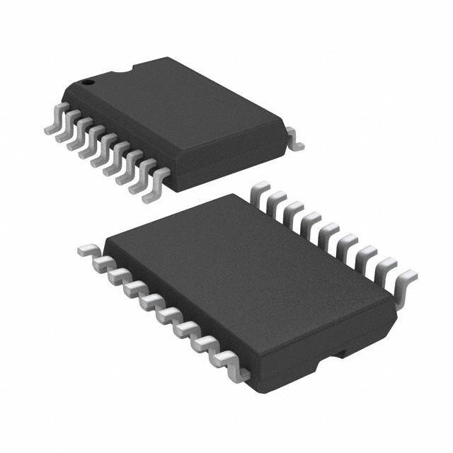
| 产品图片 |
|
| rohs | 符合RoHS无铅 / 符合限制有害物质指令(RoHS)规范要求 |
| 产品系列 | 电源管理 IC,开关控制器 ,Texas Instruments UC3526DWG4- |
| 数据手册 | |
| 产品型号 | UC3526DWG4 |
| PWM类型 | 电压模式 |
| 上升时间 | 300 ns |
| 下降时间 | 100 ns |
| 产品种类 | 开关控制器 |
| 倍增器 | 无 |
| 分频器 | 无 |
| 包装 | 管件 |
| 升压 | 是 |
| 占空比 | 49% |
| 占空比-最大 | 50 % |
| 反向 | 无 |
| 反激式 | 是 |
| 同步管脚 | Yes |
| 商标 | Texas Instruments |
| 安装风格 | SMD/SMT |
| 封装 | Tube |
| 封装/外壳 | 18-SOIC(0.295",7.50mm 宽) |
| 封装/箱体 | SOIC-18 Wide |
| 工作温度 | 0°C ~ 70°C |
| 工厂包装数量 | 40 |
| 开关频率 | 450 kHz |
| 拓扑结构 | Boost, Flyback, Forward, Full-Bridge, Half-Bridge, Push-Pull |
| 最大工作温度 | + 70 C |
| 最小工作温度 | 0 C |
| 标准包装 | 40 |
| 电压-电源 | 8 V ~ 35 V |
| 类型 | Voltage Mode PWM Controllers |
| 系列 | UC3526 |
| 输出数 | 2 |
| 输出电流 | 100 mA |
| 输出端数量 | 2 Output |
| 降压 | 无 |
| 隔离式 | 无 |
| 频率-最大值 | 400kHz |


- 商务部:美国ITC正式对集成电路等产品启动337调查
- 曝三星4nm工艺存在良率问题 高通将骁龙8 Gen1或转产台积电
- 太阳诱电将投资9.5亿元在常州建新厂生产MLCC 预计2023年完工
- 英特尔发布欧洲新工厂建设计划 深化IDM 2.0 战略
- 台积电先进制程称霸业界 有大客户加持明年业绩稳了
- 达到5530亿美元!SIA预计今年全球半导体销售额将创下新高
- 英特尔拟将自动驾驶子公司Mobileye上市 估值或超500亿美元
- 三星加码芯片和SET,合并消费电子和移动部门,撤换高东真等 CEO
- 三星电子宣布重大人事变动 还合并消费电子和移动部门
- 海关总署:前11个月进口集成电路产品价值2.52万亿元 增长14.8%


PDF Datasheet 数据手册内容提取
UC1526 UC2526 UC3526 Regulating Pulse Width Modulator FEATURES DESCRIPTION • 8 To 35V Operation The UC1526 is a high performance monolithic pulse width modulator circuit designed for fixed-frequency switching regulators and other • 5V Reference Trimmed To – 1% power control applications. Included in an 18-pin dual-in-line pack- • 1Hz To 400kHz Oscillator Range age are a temperature compensated voltage reference, sawtooth os- cillator, error amplifier, pulse width modulator, pulse metering and • Dual 100mA Source/Sink Outputs setting logic, and two low impedance power drivers. Also included • Digital Current Limiting are protective features such as soft-start and under-voltage lockout, digital current limiting, double pulse inhibit, a data latch for single • Double Pulse Suppression pulse metering, adjustable deadtime, and provision for symmetry cor- • Programmable Deadtime rection inputs. For ease of interface, all digital control ports are TTL and B-series CMOS compatible. Active LOW logic design allows • Under-Voltage Lockout wired-OR connections for maximum flexibility. This versatile device • Single Pulse Metering can be used to implement single-ended or push-pull switching regu- lators of either polarity, both transformerless and transformer cou- • Programmable Soft-Start pled. The UC1526 is characterized for operation over the full military • Wide Current Limit Common Mode Range temperature range of -55°C to +125°C. The UC2526 is characterized for operation from -25°C to +85°C, and the UC3526 is characterized • TTL/CMOS Compatible Logic Ports for operation from 0° to +70°C. • Symmetry Correction Capability • Guaranteed 6 Unit Synchronization BLOCK DIAGRAM 6/93
UC1526 UC2526 UC3526 ABSOLUTE MAXIMUM RATINGS (Note 1, 2) RECOMMENDED OPERATING CONDITIONS (Note 3) Input Voltage (+VIN). . . . . . . . . . . . . . . . . . . . . . . . . . . . . . +40V Input Voltage . . . . . . . . . . . . . . . . . . . . . . . . . . . . . . +8V to +35V Collector Supply Voltage (+VC) . . . . . . . . . . . . . . . . . . . . . +40V Collector Supply Voltage. . . . . . . . . . . . . . . . . . . +4.5V to +35V Logic Inputs . . . . . . . . . . . . . . . . . . . . . . . . . . . . . -0.3V to +5.5V Sink/Source Load Current (each output). . . . . . . . . 0 to 100mA Analog Inputs . . . . . . . . . . . . . . . . . . . . . . . . . . . . . -0.3V to +VIN Reference Load Current . . . . . . . . . . . . . . . . . . . . . . 0 to 20mA Source/Sink Load Current (each output). . . . . . . . . . . . . 200mA Oscillator Frequency Range . . . . . . . . . . . . . . . . 1Hz to 400kHz Reference Load Current. . . . . . . . . . . . . . . . . . . . . . . . . . . 50mA Oscillator Timing Resistor . . . . . . . . . . . . . . . . . . . 2kW to 150kW Logic Sink Current . . . . . . . . . . . . . . . . . . . . . . . . . . . . . . . 15mA Oscillator Timing Capacitor . . . . . . . . . . . . . . . . . . . 1nF to 20m F Power Dissipation at TA = +25°C (Note 2). . . . . . . . . . 1000mW Available Deadtime Range at 40kHz. . . . . . . . . . . . . 3% to 50% Power Dissipation at TC = +25°C (Note 2). . . . . . . . . . 3000mW Operating Ambient Temperature Range Operating Junction Temperature. . . . . . . . . . . . . . . . . . +150°C UC1526 . . . . . . . . . . . . . . . . . . . . . . . . . . . . -55°C to +125°C Storage Temperature Range. . . . . . . . . . . . . . -65°C to +150°C UC2526 . . . . . . . . . . . . . . . . . . . . . . . . . . . . . -25°C to +85°C Lead Temperature (soldering, 10 seconds). . . . . . . . . . +300°C UC3526 . . . . . . . . . . . . . . . . . . . . . . . . . . . . . . -0°C to +70°C Note 1:Values beyond which damage may occur. Note3:Range over which the device is functional and Note 2:Consult packaging section of databook for thermal parameter limits are guaranteed. limitations and considerations of package. CONNECTION DIAGRAMS DIL-18, SOIC-18 (TOP VIEW) PLCC-20, LCC-20 PACKAGE PIN FUNCTION J or N Package, DW Package (TOP VIEW) FUNCTION PIN Q and L Packages N/C 1 +Error 2 -Error 3 Comp. 4 C__S_S___ 5 Reset 6 - Current Sense 7 +__ C__u_rr_e_n_t_ Sense 8 Shutdown 9 RTIMING 10 CT 11 RD 12 Sync 13 Output A 14 VC 15 N/C 16 Ground 17 Output B 18 +VIN 19 VREF 20 ELECTRICAL CHARACTERISTICS:+VIN = 15V, and over operating ambient temperature, unless otherwise specified, TA = TJ. PARAMETER TEST CONDITIONS UC1526 / UC2526 UC3526 UNITS MIN TYP MAX MIN TYP MAX Reference Section (Note 4) Output Voltage TJ = + 25°C 4.95 5.00 5.05 4.90 5.00 5.10 V Line Regulation +VIN = 8 to 35V 10 20 10 30 mV Load Regulation IL = 0 to 20mA 10 30 10 50 mV Temperature Stability Over Operating TJ 15 50 15 50 mV Total Output Over Recommended 4.90 5.00 5.10 4.85 5.00 5.15 V Voltage Range Operating Conditions Short Circuit Current VREF = 0V 25 50 100 25 50 100 mA Un_d_e_r_ _-V__oltage Lockout RESET Output Voltage VREF = 3.8V 0.2 0.4 0.2 0.4 V VREF = 4.8V 2.4 4.8 2.4 4.8 V Note 4: IL = 0mA. 2
UC1526 UC2526 UC3526 ELECTRICAL CHARACTERISTICS:+VIN = 15V, and over operating ambient temperature, unless otherwise specified, TA = TJ. PARAMETER TEST CONDITIONS UC1526 / UC2526 UC3526 UNITS MIN TYP MAX MIN TYP MAX Oscillator Section (Note 5) Initial Accuracy TJ = + 25°C – 3 – 8 – 3 – 8 % Voltage Stability +VIN = 8 to 35V 0.5 1 0.5 1 % Temperature Stability Over Operating TJ 7 10 3 5 % Minimum Frequency RT = 150kWW , CT = 20mm F 1 1 Hz Maximum Frequency RT = 2kWW , CT = 1.0nF 400 400 kHz Sawtooth Peak Voltage +VIN = 35V 3.0 3.5 3.0 3.5 V Sawtooth Valley Voltage +VIN = 8V 0.5 1.0 0.5 1.0 V Error Amplifier Section (Note 6) Input Offset Voltage RS ££ 2kWW 2 5 2 10 mV Input Bias Current -350 -1000 -350 -2000 nA Input Offset Current 35 100 35 200 nA DC Open Loop Gain RL ‡ 10MWW 64 72 60 72 dB HIGH Output Voltage VPIN1-VPIN2 ‡‡ 150mV, ISOURCE = 3.6 4.2 3.6 4.2 V 100mm A LOW Output Voltage VPIN2-VPIN1 ‡‡ 150mV, ISINK = 100mm A 0.2 0.4 0.2 0.4 V Common Mode Rejection Rs £ 12kW 70 94 70 94 dB Supply Voltage Rejection +VIN = 12 to 18V 66 80 66 80 dB PWM Comparator (Note 5) Minimum Duty Cycle VCOMPENSATION = +0.4V 0 0 % Maximum Duty Cycle VCOMPENSATION = +3.6V 45 49 45 49 % Digital Ports (SYNC, SHUTDOWN, and RESET) HIGH Output Voltage ISOURCE =40mm A 2.4 4.0 2.4 4.0 V LOW Output Voltage ISINK = 3.6mA 0.2 0.4 0.2 0.4 V HIGH Input Current VIH = +2.4V -125 -200 -125 -200 m A LOW Input Current VIL = +0.4V -225 -360 -225 -360 m A Current LImit Comparator (Note 7) Sense Voltage RS ££ 50WW 90 100 110 80 100 120 mV Input Bias Current -3 -10 -3 -10 m A Soft-Start Section Error Clamp Voltage RESET = +0.4V 0.1 0.4 0.1 0.4 V Cs Charging Current RESET =+2.4V 50 100 150 50 100 150 m A Output Drivers (Each Output) (Note 8) HIGH Output Voltage ISOURCE = 20mA 12.5 13.5 12.5 13.5 V ISOURCE = 100mA 12 13 12 13 V LOW Output Voltage ISINK = 20mA 0.2 0.3 0.2 0.3 V ISINK = 100mA 1.2 2.0 1.2 2.0 V Collector Leakage VC = 40V 50 150 50 150 m A Rise Time CL = 1000pF 0.3 0.6 0.3 0.6 m s Fall Time CL = 1000pF 0.1 0.2 0.1 0.2 m s Power Consumption (Note 9) ____________ Standby Current SHUTDOWN = +0.4V 18 30 18 30 mA Note 4: IL = 0mA. Note 6: VCM = 0 to +5.2V Note 5: FOSC = 40kHz (RT = 4.12k W– 1%, CT = 0.1m F – 1%, Note 8: VC = +15V RD = 0W ) Note 9: +VIN = +35V, RT = 4.12kW 3
UC1526 UC2526 UC3526 APPLICATIONS INFORMATION Voltage Reference The reference regulator of the UC1526 is based on a tem- perature compensated zener diode. The circuitry is fully active at supply voltages above +8V, and provides up to 20mA of load current to external circuitry at +5.0V. In sys- tems where additional current is required, an external PNP transistor can be used to boost the available current. A rugged low frequency audio-type transistor should be used, and lead lengths between the PWM and transistor should be as short as possible to minimize the risk of os- cillations. Even so, some types of transistors may require collector-base capacitance for stability. Up to 1 amp of load current can be obtained with excellent regulation if Figure 2. Under-Voltage Lockout Schematic the device selected maintains high current gain. Soft-Start Circuit The soft-start circuit protects the power transistors and rectifier diodes from high current surges during power supply turn-on. When supply voltage is first applie_d_ t_o_ t_h_e_ UC1526, the under-voltage lockout circuit holds RESET LOW with Q3. Q1 is turned on, which holds the soft-start capacitor voltage at zero. The second collector of Q1 clamps the output of the error amplifier to ground, guaran- teeing zero duty cycle at the driver outputs. Wh_e__n_ _th__e supply voltage reaches normal operating range, RESET Figure 1. Extending Reference Output Current will go HIGH. Q1 turns off, allowing the internal 100mA current source to charge CS. Q2 clamps the error ampli- Under-Voltage Lockout fier output to 1VBE above the voltage on CS. As the soft- The under-voltage lockout circuit protects the UC1526 start voltage ramps up to +5V, the duty cycle of the PWM and the power devices it controls from inadequate supply linearly increases to whatever value the voltage regula- voltage, If +VIN is too lo_w_,_ _th_e__ circuit disables the output tion loop requires for an error null. drivers and holds the RESET pin LOW. This prevents spurious output pulses while the control circuitry is stabi- lizing, and holds the soft-start timing capacitor in a dis- charged state. The circuit consists of a +1.2V bandgap reference and comparator circuit which is active when the reference voltage has risen to 3VBE or +1.8V at 25°C. When the ref- erence voltage rises to approximately +4.4V_,_ t_h_e_ _c_ircuit enables the output drivers and releases the RESET pin, allowing a normal soft-start. The comparator has 200mV of hysteresis to minimize oscillation at the trip point. When +VIN to the PWM is removed and the re_fe_r_e_n_c_e_ drops to +4.2V, the under-voltage circuit pulls RESET LOW again. The soft-start capacitor is immediately dis- Figure 3. Soft-Start Circuit Schematic charged, and the PWM is ready for another soft-start cy- Digital Control Ports cle. The three digital control ports of the UC1526 are bi-direc- The UC1526 can operate from a +5V supply by connect- tional. Each pin can drive TTL and 5V CMOS logic di- ing the VREF pin to the +VIN pin and maintaining the sup- rectly, up to a fan-out of 10 low-power Schottky gates. ply between +4.8 and +5.2V. Each pin can also be directly driven by open-collector 4
UC1526 UC2526 APPLICATIONS INFORMATION (cont.) UC3526 TTL, open-drain CMOS, and open-collector voltage com- Multiple devices can be synchronized together by pro- parators; fan-in is equivalent to 1 low-power Schottky gramming one master unit for the desired frequency and gate. Each port is normally HIGH; the pin_ _is_ _p_u_lled LOW then sharing its sawtooth and clock waveforms with the to activate the particular function. Driving SYNC LOW in- slave units. All CT term__in_a_l_s_ are connected to the CT pin i_t_ia_t_e_s_ __a_ __d_ischarge cycle in the oscillator. Pulling of the master, _a_n_d_ __all SYNC terminals are likewise con- SHUTDOWN LOW__ _im__m__ediately inhibits all PWM output nected to the SYNC pin of the master. Slave RT termi- pulses. Holding RESET LOW discharges the soft-start nals are left open or connected to VREF. Slave RD capacitor. The logic threshold is +1.1V at +25°C. Noise terminals may be either left open or grounded. immunity can be gained at the expense of fan-out with an Error Amplifier external 2k pull-up resistor to +5V. The error amplifier is a transconductance design, with an output impedance of 2MW . Since all voltage gain takes place at the output pin, the open-loop gain/frequency characteristics can be controlled with shunt reactance to ground. When compensated for unity-gain stability with 100pF, the amplifier has an open-loop pole at 800Hz. The input connections to the error amplifier are deter- mined by the polarity of the switching supply output volt- age. For positive supplies, the common-mode voltage is +5.0V and the feedback connections in Figure 6A are used. With negative supplies, the common-mode voltage Figure 4. Digital Control Port Schematic is ground and the feedback divider is connected between the negative output and the +5.0V reference voltage, as Oscillator shown in Figure 6B. The oscillator is programmed for frequency and dead time Output Drivers with three components: RT, CT and RD. Two waveforms are generated: a sawtooth waveform at pin 10 for pulse The totem-pole output drivers of the UC1526 are de- width modulation, and a logic clock at pin 12. The follow- signed to source and sink 100mA continuously and ing procedure is recommended for choosing timing val- 200mA peak. Loads can be driven either from the output ues: pins 13 and 16, or from the +VC, as required. 1. With RD = 0 (pin 11 shorted to ground) select values Since the bottom transistor of the totem-pole is allowed to for RT and CT from Figure 7 to give the desired oscillator saturate, there is a momentary conduction path from the period. Remember that the frequency at each driver out- +VC terminal to ground during switching. To limit the re- put is half the oscillator frequency, and the frequency at sulting current spikes a small resistor in series with pin 14 the +VC terminal is the same as the oscillator frequency. is always recommended. The resistor value is deter- mined by the driver supply voltage, and should be chosen 2. If more dead time is required, select a large value of for 200mA peak currents. RD. At 40kHz dead time increases by 400ns/W . 3. Increasing the dead time will cause the oscillator fre- quency to decrease slightly. Go back and decrease the value of RT slightly to bring the frequency back to the nominal design value. The UC1526 can be synchronized to an external logic clock by programming the oscillator to free-run at a fre- quency 10% slower than the sync frequency. A pe_r_io__d_i_c LOW logic pulse approximately 0.5m s wide at the SYNC pin will then lock the oscillator to the external frequency. Figure 5. Oscillator Connections and Waveforms 5
UC1526 UC2526 UC3526 Figure 6. Error Amplifier Connections Figure 8. Single-Ended Configuration Figure 7. Push-Pull Configuration Figure 9. Driving N-channel Power Mosfets TYPICAL CHARACTERISTICS Oscillator Period vs RT and CT Oscillation Period 6
UC1526 UC2526 UC3526 TYPICAL CHARACTERISTICS Output Driver Deadtime vs RD Value Under Voltage Lockout Characteristic Error Amplifier Open Loop Gain vs Frequency Current Limit Transfer Function Shutdown Delay Output Driver Saturation Voltage UNITRODE INTEGRATED CIRCUITS 7 CONTINENTAL BLVD. • MERRIMACK, NH 03054 TEL. (603) 424-2410 • FAX (603) 424-3460 7
PACKAGE OPTION ADDENDUM www.ti.com 6-Feb-2020 PACKAGING INFORMATION Orderable Device Status Package Type Package Pins Package Eco Plan Lead/Ball Finish MSL Peak Temp Op Temp (°C) Device Marking Samples (1) Drawing Qty (2) (6) (3) (4/5) 8551501VA ACTIVE CDIP J 18 1 TBD Call TI N / A for Pkg Type -55 to 125 8551501VA UC1526J/883B UC1526J ACTIVE CDIP J 18 1 TBD Call TI N / A for Pkg Type -55 to 125 UC1526J UC1526J883B ACTIVE CDIP J 18 1 TBD Call TI N / A for Pkg Type -55 to 125 8551501VA UC1526J/883B UC2526AJ ACTIVE CDIP J 18 1 TBD Call TI N / A for Pkg Type -25 to 85 UC2526AJ UC2526N ACTIVE PDIP N 18 20 Green (RoHS NIPDAU N / A for Pkg Type -25 to 85 UC2526N & no Sb/Br) UC3526AJ ACTIVE CDIP J 18 1 TBD Call TI N / A for Pkg Type 0 to 70 UC3526AJ UC3526DW ACTIVE SOIC DW 18 40 Green (RoHS NIPDAU Level-2-260C-1 YEAR 0 to 70 UC3526DW & no Sb/Br) UC3526DWTR ACTIVE SOIC DW 18 2000 Green (RoHS NIPDAU Level-2-260C-1 YEAR 0 to 70 UC3526DW & no Sb/Br) UC3526N ACTIVE PDIP N 18 20 Green (RoHS NIPDAU N / A for Pkg Type 0 to 70 UC3526N & no Sb/Br) UC3526NG4 ACTIVE PDIP N 18 20 Green (RoHS NIPDAU N / A for Pkg Type 0 to 70 UC3526N & no Sb/Br) (1) The marketing status values are defined as follows: ACTIVE: Product device recommended for new designs. LIFEBUY: TI has announced that the device will be discontinued, and a lifetime-buy period is in effect. NRND: Not recommended for new designs. Device is in production to support existing customers, but TI does not recommend using this part in a new design. PREVIEW: Device has been announced but is not in production. Samples may or may not be available. OBSOLETE: TI has discontinued the production of the device. (2) RoHS: TI defines "RoHS" to mean semiconductor products that are compliant with the current EU RoHS requirements for all 10 RoHS substances, including the requirement that RoHS substance do not exceed 0.1% by weight in homogeneous materials. Where designed to be soldered at high temperatures, "RoHS" products are suitable for use in specified lead-free processes. TI may reference these types of products as "Pb-Free". RoHS Exempt: TI defines "RoHS Exempt" to mean products that contain lead but are compliant with EU RoHS pursuant to a specific EU RoHS exemption. Green: TI defines "Green" to mean the content of Chlorine (Cl) and Bromine (Br) based flame retardants meet JS709B low halogen requirements of <=1000ppm threshold. Antimony trioxide based flame retardants must also meet the <=1000ppm threshold requirement. (3) MSL, Peak Temp. - The Moisture Sensitivity Level rating according to the JEDEC industry standard classifications, and peak solder temperature. Addendum-Page 1
PACKAGE OPTION ADDENDUM www.ti.com 6-Feb-2020 (4) There may be additional marking, which relates to the logo, the lot trace code information, or the environmental category on the device. (5) Multiple Device Markings will be inside parentheses. Only one Device Marking contained in parentheses and separated by a "~" will appear on a device. If a line is indented then it is a continuation of the previous line and the two combined represent the entire Device Marking for that device. (6) Lead/Ball Finish - Orderable Devices may have multiple material finish options. Finish options are separated by a vertical ruled line. Lead/Ball Finish values may wrap to two lines if the finish value exceeds the maximum column width. Important Information and Disclaimer:The information provided on this page represents TI's knowledge and belief as of the date that it is provided. TI bases its knowledge and belief on information provided by third parties, and makes no representation or warranty as to the accuracy of such information. Efforts are underway to better integrate information from third parties. TI has taken and continues to take reasonable steps to provide representative and accurate information but may not have conducted destructive testing or chemical analysis on incoming materials and chemicals. TI and TI suppliers consider certain information to be proprietary, and thus CAS numbers and other limited information may not be available for release. In no event shall TI's liability arising out of such information exceed the total purchase price of the TI part(s) at issue in this document sold by TI to Customer on an annual basis. OTHER QUALIFIED VERSIONS OF UC1526, UC2526AM, UC3526, UC3526AM : •Catalog: UC3526, UC2526A, UC3526M, UC3526A •Military: UC1526, UC1526A NOTE: Qualified Version Definitions: •Catalog - TI's standard catalog product •Military - QML certified for Military and Defense Applications Addendum-Page 2
IMPORTANTNOTICEANDDISCLAIMER TI PROVIDES TECHNICAL AND RELIABILITY DATA (INCLUDING DATASHEETS), DESIGN RESOURCES (INCLUDING REFERENCE DESIGNS), APPLICATION OR OTHER DESIGN ADVICE, WEB TOOLS, SAFETY INFORMATION, AND OTHER RESOURCES “AS IS” AND WITH ALL FAULTS, AND DISCLAIMS ALL WARRANTIES, EXPRESS AND IMPLIED, INCLUDING WITHOUT LIMITATION ANY IMPLIED WARRANTIES OF MERCHANTABILITY, FITNESS FOR A PARTICULAR PURPOSE OR NON-INFRINGEMENT OF THIRD PARTY INTELLECTUAL PROPERTY RIGHTS. These resources are intended for skilled developers designing with TI products. You are solely responsible for (1) selecting the appropriate TI products for your application, (2) designing, validating and testing your application, and (3) ensuring your application meets applicable standards, and any other safety, security, or other requirements. These resources are subject to change without notice. TI grants you permission to use these resources only for development of an application that uses the TI products described in the resource. Other reproduction and display of these resources is prohibited. No license is granted to any other TI intellectual property right or to any third party intellectual property right. TI disclaims responsibility for, and you will fully indemnify TI and its representatives against, any claims, damages, costs, losses, and liabilities arising out of your use of these resources. TI’s products are provided subject to TI’s Terms of Sale (www.ti.com/legal/termsofsale.html) or other applicable terms available either on ti.com or provided in conjunction with such TI products. TI’s provision of these resources does not expand or otherwise alter TI’s applicable warranties or warranty disclaimers for TI products. Mailing Address: Texas Instruments, Post Office Box 655303, Dallas, Texas 75265 Copyright © 2020, Texas Instruments Incorporated