ICGOO在线商城 > 集成电路(IC) > PMIC - 稳压器 - DC DC 切换控制器 > UCC28230DRNT
 Datasheet下载
- 型号: UCC28230DRNT
- 制造商: Texas Instruments
- 库位|库存: xxxx|xxxx
- 要求:
| 数量阶梯 | 香港交货 | 国内含税 |
| +xxxx | $xxxx | ¥xxxx |
查看当月历史价格
查看今年历史价格
UCC28230DRNT产品简介:
ICGOO电子元器件商城为您提供UCC28230DRNT由Texas Instruments设计生产,在icgoo商城现货销售,并且可以通过原厂、代理商等渠道进行代购。 UCC28230DRNT价格参考。Texas InstrumentsUCC28230DRNT封装/规格:PMIC - 稳压器 - DC DC 切换控制器, 全桥,半桥,推挽 稳压器 正 输出 升压/降压 DC-DC 控制器 IC 12-USON(3x2)。您可以下载UCC28230DRNT参考资料、Datasheet数据手册功能说明书,资料中有UCC28230DRNT 详细功能的应用电路图电压和使用方法及教程。
Texas Instruments(德州仪器)的UCC28230DRNT是一款高性能的PMIC(电源管理集成电路),属于DC-DC切换控制器类别,主要应用于需要高效能和高可靠性电源转换的场景。以下是其典型应用场景:

1. 工业设备:UCC28230DRNT适用于工业自动化设备、可编程逻辑控制器(PLC)、伺服驱动器等需要稳定电压输出的场合。它能够提供高效的功率转换,支持复杂的工业系统运行。

2. 通信基础设施:在基站、路由器和交换机等通信设备中,该芯片用于实现高效的电源管理,确保设备长时间稳定运行,同时降低功耗和热量产生。

3. 太阳能逆变器:作为新能源领域的重要组成部分,UCC28230DRNT可用于太阳能逆变器中的电源管理模块,帮助优化能量转换效率,提升系统的整体性能。

4. 汽车电子:在电动汽车(EV)和混合动力汽车(HEV)中,这款芯片可以用于车载充电器、DC-DC转换器以及电池管理系统(BMS),以满足汽车级的严格要求。

5. 消费电子产品:如笔记本电脑适配器、平板电脑充电器等便携式设备中,UCC28230DRNT能够提供快速充电功能,同时保持较小的体积和较低的成本。

6. 医疗设备:在便携式医疗设备(如血压计、血糖仪)或大型医疗成像设备(如CT扫描仪、MRI)中,该芯片确保了电源的精确控制和低噪声特性,从而提高诊断精度。

7. LED照明:在大功率LED照明系统中,UCC28230DRNT可以实现恒流驱动,保证LED灯的亮度一致性和长寿命。

总结来说,UCC28230DRNT凭借其高效、灵活和可靠的特性,广泛应用于工业、通信、新能源、汽车、消费电子、医疗和照明等多个领域,为各种复杂系统提供稳定的电源解决方案。
| 参数 | 数值 |
| 产品目录 | 集成电路 (IC) |
| Cuk | 无 |
| 描述 | IC REG CTRLR PWM VM 12-SON |
| 产品分类 | |
| 品牌 | Texas Instruments |
| 数据手册 | |
| 产品图片 |
|
| 产品型号 | UCC28230DRNT |
| PWM类型 | 电压模式 |
| rohs | 无铅 / 符合限制有害物质指令(RoHS)规范要求 |
| 产品系列 | - |
| 倍增器 | 无 |
| 其它名称 | 296-23560-1 |
| 分频器 | 无 |
| 包装 | 剪切带 (CT) |
| 升压 | 无 |
| 占空比 | 100% |
| 反向 | 无 |
| 反激式 | 无 |
| 封装/外壳 | 12-UFDFN 裸露焊盘 |
| 工作温度 | -55°C ~ 125°C |
| 标准包装 | 1 |
| 电压-电源 | 7 V ~ 17 V |
| 输出数 | 4 |
| 配用 | /product-detail/zh/UCC28230EVM/296-31340-ND/2048163 |
| 降压 | 无 |
| 隔离式 | 无 |
| 频率-最大值 | 1MHz |


PDF Datasheet 数据手册内容提取
UCC28230 UCC28231 www.ti.com................................................................................................................................................... SLUS814A–FEBRUARY2008–REVISEDJUNE2008 Advanced PWM Controller for Bus Converters FEATURES 1 • Programmable,LoadDependedOffTime DESCRIPTION Control The UCC28230, UCC28231 PWM bus controllers are • FrequencyControlledStartUpAllowsSmall optimized for use in high efficiency, high power OutputInductor,LowRippleandConstant density, unregulated intermediate bus converters. CurrentStartwithLargeOutputCapacitor Topologies include push-pull, half-bridge and full-bridge. External drivers, such as the UCC27200 • Two0.2-APush-PullOutputsProvideMatched 120-V high-side/low-side drivers, can be used with ControlSignalsDtoExternalDrivers thiscontroller. • TwoAdditional1-DOutputsforOptimalUse Low cost, small size and highly efficient solutions are ofSelf-DrivenorControlDrivenSynchronous providedbyinnovationssuchas: Rectifiers • Start-upfrequencycontrolcircuitallowingsmall • Unregulated,FixedVolt-SecondorFixed outputinductorandtheabilitytostartwithlarge FrequencyModessetbyUser intermediatebuscapacitor. • Two,1.5%OverallAccuracyReferenceVoltage • Loaddependedoff-timecontrolsetbyuser. Options:5-VforUCC28230and3.3-Vfor Additional 1-D control outputs can be used for UCC28231 primary winding clamping in self-driven output • ResistorProgrammableSwitchingFrequency synchronous rectifier applications or as drive signals upto1MHz forthecontrol-drivensynchronousrectifier. • Cycle-by-CycleCurrentLimitAllowsParallel Cycle-by-cycle current limit prevents overstresses of OperationwithDroopBasedCurrentSharing converter. If the over current condition causes less • SingleExternalCapacitorsetsSoft-Startand than 80% duty cycle at the output, then after a OverCurrentHiccupModeParameterswith programmed time the controller proceeds into Restart periodicalshutdownandrestarthiccupmode. • SevereShortCircuitHiccupwithRestartor The UCC28230 provides 5 V, and the UCC28231 LatchOffProtectionOptionbyExternal provides3.3-Vprecisionreferencevoltages with 1.5% Resistor overall accuracy and 10-mA output current. This reference voltage can be used to supply • InputUnderVoltageLockOut housekeeping circuit and/or microcontroller. The • ThermalShutdown precision reference voltage can also be used for • ThermallyEnhanced3mm×2mmSON-12 accuratesettingofsystemparameters. andTSSOP-14PackageOptions Other features include under-voltage lockout, thermal shut down, programmable soft start, over-current APPLICATIONS hiccup mode and short circuit protection with internal • IntermediateBusIsolatedConverters restart by default that can be set into latch-off mode • DC-to-DCTransformers byanexternalresistor. 1 Pleasebeawarethatanimportantnoticeconcerningavailability,standardwarranty,anduseincriticalapplicationsofTexas Instrumentssemiconductorproductsanddisclaimerstheretoappearsattheendofthisdatasheet. PRODUCTIONDATAinformationiscurrentasofpublicationdate. Copyright©2008,TexasInstrumentsIncorporated Products conform to specifications per the terms of the Texas Instruments standard warranty. Production processing does not necessarilyincludetestingofallparameters.
UCC28230 UCC28231 SLUS814A–FEBRUARY2008–REVISEDJUNE2008................................................................................................................................................... www.ti.com TYPICAL APPLICATION DIAGRAMS + Vbias Vbias UCC27200 UCC27200 VDD VDD Vin HB HB CT 36V to60V HI HO HO HI HS HS LI LO LO LI VSS VSS _ + Vout 7V to12V 400W Bias _ Power Vbias Supply VDD VDD CUoVmLpO. SThhuetrdmoawln VDD 12 EN Reference Interface Vcc=5V or3.3V R1 VREOFS3165..37VV r fisaOellffTime 5VLV/3DD.DO3V Generator 10O1_DIN Sywsittehm Housekeeping R2 OSRT32 CCiorcnutriotl SShhourtt dCoirwcnuit 8O2_DIN CS Micro 6 Is Controller CCycylcel eCub-ryren-t BLologcikc 11O1_D Limit O2_D Oscillator& CLK 9 Vin RT Start Up Soft Start & 4 Frequency Hiccup Current GND Control Limit Circuit 7 5 SS Figure1.Full-BridgeBusConverter + Vbias UCC27200 VDD Vin HB CT 36V to 60V HI HO HS LI LO VSS _ + Vout 7V to 12V 200W Bias _ Power Vbias Supply UCC28230/1 Vbias VDD VDD CUoVmLpO. SThhuetrdmoawln VDD ISnytwesrittfehamce HouskVecce =p5iVn ogr 3.3V RR12 OVRSROTE3SF1123265..37VV r fisaOelClCfiforTcnuitmritoel 5VLV/3DD.DO3VSShhourtt dCoiwrcnuit EN RGeefneererantcoer 180OO21__DDIINN IINNAB24 6VDD 75OOUUTTAB CoMnictrrool-ler CS6 Is Logic O1_D 3GND Cycleb-y - Block 11 Cycle Current UCC27324 Limit O2_D Oscillator& CLK 9 Vin RT Start Up Soft Start & 4 Frequency Hiccup Current GND Control Limit Circuit 7 5 SS Figure2.Half-BridgeBusConverterwithControl-DrivenSynchronousRectifier 2 SubmitDocumentationFeedback Copyright©2008,TexasInstrumentsIncorporated ProductFolderLink(s):UCC28230UCC28231
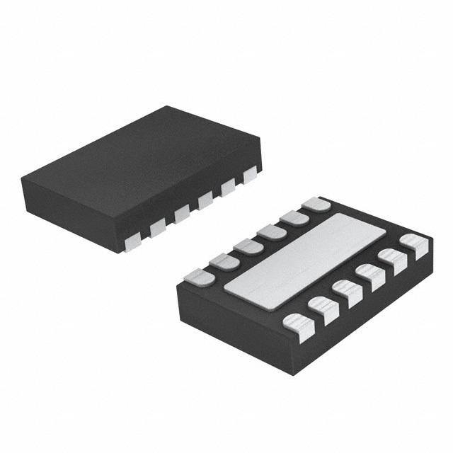
UCC28230 UCC28231 www.ti.com................................................................................................................................................... SLUS814A–FEBRUARY2008–REVISEDJUNE2008 PINOUT CONFIGURATION ORDERINGINFORMATION(1) (2) TEMPERATURERANGE, REFERENCEVOLTAGE PACKAGE TAPEandREELQTY PARTNUMBER T =T A J 5V .250 UCC28230DRNT 5V 3000 UCC28230DRNR Plastic12-pinSON(DRN) 3.3V 250 UCC28231DRNT 3.3V 3000 UCC28231DRNR –55°Cto+125°C 5V 250 UCC28230PW 5V 2000 UCC28230PWR Plastic14-pinTSSOP(PW) 3.3V 250 UCC28231PW 3.3V 2000 UCC28231PWR (1) The12-pinSON(DRN)and14-pinTSSOPpackagesusePb-FreeleadfinishofPd-Ni-AuwhichiscompatiblewithMSLlevel1at 255-260°CpeakreflowtemperaturetobecompatiblewitheitherleadfreeorSn/Pbsolderingoperations. (2) ThepadunderneaththecenteroftheICisathermalsubstrate.ThePCB“thermalland”designforthisexposeddiepadshouldinclude thermalviasthatdropdownandconnecttooneormoreburiedcopperplane(s).Thiscombinationofviasforverticalheatescapeand buriedplanesforheatspreadingallowstheDRNtoachieveitsfullthermalpotential.ThispadisalsointernallyconnectedtoGNDpin. Copyright©2008,TexasInstrumentsIncorporated SubmitDocumentationFeedback 3 ProductFolderLink(s):UCC28230UCC28231
UCC28230 UCC28231 SLUS814A–FEBRUARY2008–REVISEDJUNE2008................................................................................................................................................... www.ti.com ABSOLUTE MAXIMUM RATINGS overoperatingfree-airtemperaturerange (1) (2)(unlessotherwisenoted) PARAMETER VALUE UNIT V (3) Inputsupplyvoltagerange –0.3to20.0 DD O1_D,O2_D,O1_DIN,O2_DIN –0.3toV +0.3 DD InputsvoltagesonOS,CS,SS,RT,OST –0.3to6.3 V OutputvoltageonVREF –0.3to5.6 HBM 2k ESDrating CDM 500 Continuoustotalpowerdissipation SeeDissipationRatingTable T Operatingvirtualjunctiontemperaturerange –55to+150 J T Operatingambienttemperaturerange –55to+125 A °C T StorageTemperature –65to+150 stg LeadTemperature(Soldering,10sec.)PWPackage +300 (1) Stressesbeyondthoselistedunderabsolutemaximumratingsmaycausepermanentdamagetothedevice.Thesearestressratings only,andfunctionaloperationofthedeviceattheseoranyotherconditionsbeyondthoseindicatedunderrecommendedoperating conditionsisnotimplied.Exposuretoabsolute-maximum-ratedconditionsforextendedperiodsmayaffectdevicereliability. (2) Thesedevicesaresensitivetoelectrostaticdischarge;followproperdevicehandlingprocedures. (3) AllvoltagesarewithrespecttoGNDunlessotherwisenoted.Currentsarepositiveinto,negativeoutofthespecifiedterminal.See PackagingSectionofthedatasheetforthermallimitationsandconsiderationsofpackages. DISSIPATION RATINGS(1) q JC(°C/W) q JA(°C/W) q (°C/W) q JB(°C/W) BOARD PACKAGE JUNCTIONTO JUNCTIONTO JP JUNCTIONTO JUNCTIONTOPAD CASE AMBIENT BOARD High-K(2) DRN 70.66 15 37.66 PW 2.71 97.65 2.07 (1) ThesethermaldataaretakenatstandardJEDECtestconditionsandareusefulforthethermalperformancecomparisonofdifferent packages.ThecoolingconditionandthermalimpedanceRq JAofpracticaldesignisspecific. (2) TheJEDECtestboardJESD51-5withdirectthermalpadattach,3-inch×3-inch,4-layerwith1-ozinternalpowerandgroundplanesand 2-oztopandbottomtracelayers(preliminarydatabasedonmodeling) RECOMMENDED OPERATING CONDITIONS MIN NOM MAX UNIT V Supplyvoltagerange 7 12 17 V DD Operatingjunctiontemperaturerange –55 125 °C 4 SubmitDocumentationFeedback Copyright©2008,TexasInstrumentsIncorporated ProductFolderLink(s):UCC28230UCC28231
UCC28230 UCC28231 www.ti.com................................................................................................................................................... SLUS814A–FEBRUARY2008–REVISEDJUNE2008 ELECTRICAL CHARACTERISTICS(1) V =12V,1-m FcapacitorfromV andVREFtoGND,T =T =–55°Cto125°C,RT=49.9kΩconnectedto4.4Vsupplyto DD DD A J setFsw=100kHz(unlessotherwisenoted). PARAMETER TESTCONDITIONS MIN TYP MAX UNIT SupplyCurrents IDDD(off) Startupcurrent VDD=5.2V 150 200 m A IDD Operatingsupplycurrent 1.5 2.5 mA UnderVoltageLockout Startthreshold 5.9 6.3 6.9 Minimumoperatingvoltageafterstart 5.3 5.7 6.2 V Hysteresis 0.55 0.6 0.75 SoftStart(SSPIN,Figure41,Figure44) ISS Chargecurrent VSS=0V –30 –25 –20 m A VSS_STD Shutdown/restart/resetthreshold 0.3 0.55 0.68 VSS_FP Soft-startfirstpulsethreshold 0.68 0.85 1.1 V VSS_PU Pullupthreshold 3.3 3.5 3.8 VSS_CL Clampvoltage 4.3 4.5 4.8 Off-TimeProgramming(Figure33) TOFF5 OfftimebetweenO1_DandO2_D UCC28230 32 40 50 TOFF3 OfftimebetweenO1_DandO2_D UCC28231 30 40 53 OS=8.45kΩ,CS=0.3V,OST=1V TDT DeadtimebetweenO1_D,O1_DINandO2_D,O2_DIN 10 16 ΔTOFF Offtimematching 2 ns TOFFR5 OfftimebetweenO1_DandO2_D UCC28230 32 40 50 TOFFR3 OfftimebetweenO1_DandO2_D UCC28231 30 40 53 OS=8.45kΩ,CS=0V,OST=VREF TDTREF DeadtimebetweenO1_D,O1_DINandO2_D,O2_DIN 10 16 ΔTOFFR Offtimematching 2 IHYST Hysteresiscurrentsource 10 m A TOFFMAX MaximumofftimeatlowCS OVS=8.45kΩ,OST=1V,CS=CSTH–0.03 165 235 ns SwitchingFrequencyatO1_DandO2_DOutputs FSWNOM Nominalfrequency VSS=4V 92 100 108 kHz FSWMAX Maximumfrequency VSS=1.8V 425 550 675 VREFOutputVoltage VREF5 VREFtotaloutputrange UCC28230 0≤IR≤10mA;VDD=from7Vto17V, 4.925 5 5.075 V VREF3 UCC28231 –55°C≤TJ≤125°C 3.25 3.3 3.35 ISCC Shortcircuitcurrent VREF=0V –35 –25 –12 mA (1) TypicalvaluesforT =25°C A Copyright©2008,TexasInstrumentsIncorporated SubmitDocumentationFeedback 5 ProductFolderLink(s):UCC28230UCC28231
UCC28230 UCC28231 SLUS814A–FEBRUARY2008–REVISEDJUNE2008................................................................................................................................................... www.ti.com ELECTRICAL CHARACTERISTICS (continued) V =12V,1-m FcapacitorfromV andVREFtoGND,T =T =–55°Cto125°C,RT=49.9kΩconnectedto4.4Vsupplyto DD DD A J setFsw=100kHz(unlessotherwisenoted). PARAMETER TESTCONDITIONS MIN TYP MAX UNIT CurrentSense,Cycle-by-CycleCurrentLimitWithHiccup,ShortCircuitProtectionWithLatchOff VCS_LIM CSpincycle-by-cyclethreshold 0.48 0.5 0.515 V InputpulseatCSfrom0.3Vto0.6Vwith TCS CStoO1_DandO2_Dpropagationdelay 0.03V/nsslewrate 100 ns InputpulseatCSfrom0.3Vto0.6Vwith TBL Leadingedgeblankingtimebyinternalfilter 0.03V/nsslewrate 50 IDS D(Fisigcuhraerg4e1)currenttosetcycle-by-cyclecurrentlimitduration CS=0.6V,VSS=4V 15 20 25 m A HiccupOFFtimethreshold 3.1 3.4 3.7 V IHCC D(Fisigcuhraerg4e1,cFuirgreunrett4o4s)etHiccupModeOFFTime 1.9 2.5 3.1 m A VCS_SC CSpinshortcircuitprotectionthreshold(Figure44) 0.65 0.7 0.75 V OutputsO1_D,O2_D,O1_DIN,O2_DIN Sink/Sourcepeakcurrent(2) 0.2 A Risetime CLOAD=100pF 12 25 ns Falltime CLOAD=100pF 10 25 RSRC Outputsourceresistance IOUT=20mA 10 20 35 Ω RSINK Outputsinkresistance IOUT=20mA 5 15 30 Dutycyclematching Pins7and9pulsesmatchingatFSW=100 35 ns kHz ThermalShutdown Risingthreshold(3) 150 160 170 Fallingthreshold(3) 130 140 150 °C Hysteresis 20 (2) Outputsink/sourcepeakcurrentvalue,definedbyequationI =100pF×dV/dtwheredV/dtistakenfromtheoutputriseandfall P switchingwaveforms.Itisnottestedinproduction.Characterizationisavailableuponrequest. (3) Thermalshutdownisnottestedinproduction.Characterizationisavailableuponrequest 6 SubmitDocumentationFeedback Copyright©2008,TexasInstrumentsIncorporated ProductFolderLink(s):UCC28230UCC28231
UCC28230 UCC28231 www.ti.com................................................................................................................................................... SLUS814A–FEBRUARY2008–REVISEDJUNE2008 FUNCTIONAL BLOCK DIAGRAMS V VDD UVLO Thermal VDD DD Comp. Shutdown 12 EN Reference 6.3Vrise VDD Generator VREF 5.7Vfall 5V/3.3V O1_DIN 1 LDO R1 OS 10 3 OffTime R3 Control Circuit ShortCircuit R2 2 Shutdown O2_DIN OST 8 CS Is 6 Logic O1_D CT Cycle-by- Block 11 CycleCurrent Limit O2_D Oscillator& CLK 9 Vin RT StartUp SoftStart& 4 Frequency HiccupCurrent GND Control LimitCircuit 7 5 SS Figure3.SON-12Package V V UVLO Thermal DD V DD DD Comp. Shutdown 14 EN Reference 6.3Vrise VDD Generator VREF 5.7Vfall 5V/3.3V O1_DIN 1 LDO R1 OS 12 3 OffTime R3 Control Circuit ShortCircuit R2 2 Shutdown O2_DIN OST 10 CS Is 7 Logic O1_D CT Cycle-by- Block 13 CycleCurrent NC Limit 4 O2_D Oscillator& CLK 11 Vin RT StartUp SoftStart& 5 Frequency HiccupCurrent GND AGND Control LimitCircuit 9 8 6 SS Figure4.TSSOP-14Package Copyright©2008,TexasInstrumentsIncorporated SubmitDocumentationFeedback 7 ProductFolderLink(s):UCC28230UCC28231
UCC28230 UCC28231 SLUS814A–FEBRUARY2008–REVISEDJUNE2008................................................................................................................................................... www.ti.com TERMINALFUNCTIONS TERMINAL DFN-12 TSSOP-14 I/O FUNCTION NAME PIN# PIN# ±1.5%accurate5VforUCC28230and3.3VforUCC28231,10-mAoutputreferencevoltagewith shortcircuitprotectionthatcanbeusedforfixedswitchingfrequencysettingand/orfor 1 1 VREF O housekeepingmicrocontroller.Placedecouplingcapacitorin1m Fto2.2m Frangefromthispinto GND. Offtimecontrolthresholdpinusesaresistordividertosetcurrentlevelaspercentageofcurrent 2 2 OST I limitthreshold. NominalofftimeT anddeadtimeT setpin.Anexternalresistorconnectedbetweenthispin 3 3 OS I OFF DT andGNDsetsthedeadtimeandnominalofftime. 4 NC Notconnectedpin,TSSOP-14only. Oscillatortiminginputpin.TheexternalresistorwhichisconnectedbetweenthispinandV sets IN 4 5 RT I theoscillatorfrequencywhichvarieswithV .TyingtheexternalresistortoVREFsetsfixed IN frequencyoperationindependentofV . IN Inputtoadjustablesoft-start,andhiccupmodecircuit.Placesoft-startcapacitorfromthispinto 5 6 SS I/O GND.Theinternalcharge/dischargecurrentI andanexternalcapacitorvaluesetthesoft-start SS timing,durationofcycle-by-cyclecurrentlimitandcontrollerturn-offtimeforhiccupmodeoperation. 6 7 CS I Currentsensingpinusedforcycle-by-cyclecurrentlimit,shortcircuitprotectionandofftimecontrol. 8 AGND Analogground,TSSOP-14only. 7 9 GND Groundpinconnectedtothermalpad.Allsignalsarereferencedtothisnode. 8 10 O2_DIN O 0.2-Asink/sourceswitchingoutputpintoanexternaldriverproviding1-Dpulse. 9 11 O2_D O 0.2-Asink/sourceswitchingoutputpintoanexternaldriverprovidingDpulse. 10 12 O1_DIN O 0.2-Asink/sourceswitchingoutputpintoanexternaldriverproviding1-Dpulse. 11 13 O1_D O 0.2-Asink/sourceswitchingoutputpintoanexternaldriverprovidingDpulse. Connectthispintoa7-Vto17-Vbiassupply.Placeahighqualityatleast1-m Fceramicbypass 12 14 VDD I capacitorfromthispintoGND. 8 SubmitDocumentationFeedback Copyright©2008,TexasInstrumentsIncorporated ProductFolderLink(s):UCC28230UCC28231
UCC28230 UCC28231 www.ti.com................................................................................................................................................... SLUS814A–FEBRUARY2008–REVISEDJUNE2008 TYPICAL CHARACTERISTICS Start-upCurrentIDDoff OperatingSupplyCurrentIDD overTemperatureatVDD=5.2V overTemperatureatFSW=100kHz 1.60 165 160 1.55 155 A A µDDoff,, 150 ImDD, 1.50 I 145 1.45 140 135 1.40 -55 -35 -15 5 25 45 65 85 105 125 -55 -35 -15 5 25 45 65 85 105 125 TJ-temperature,°C TJ-temperature,°C Figure5. Figure6. UnderVoltageLockoutThresholds UnderVoltageLockoutHysteresis overTemperature overTemperature 6.7 0.70 6.5 V6.3 0.68 s, V Threshold56..91 Hysteresis,0.66 UVLO5.7 UVLO0.64 5.5 5.3 -55 -35 -15 5 25 45 65 85 105 125 0.62 TJ-temperature,°C -55 -35 -15 5 25 45 65 85 105 125 Risingthreshold Fallingthreshold TJ-temperature,°C Figure7. Figure8. SoftStartShutdownVSS_STDandFirstPulseVSS_FP SoftStartPull-upVSS_PUandClampVoltageVSS_CL ThresholdsoverTemperature ThresholdsoverTemperature 1.00 5.00 0.90 V 0.80 V 4.50 , , VSS_FP 0.70 VSS_CL 4.00 V,SS_STD 00..5600 V,SS_PU 3.50 0.40 0.30 3.00 -55 -35 -15 5 25 45 65 85 105 125 -55 -35 -15 5 25 45 65 85 105 125 TJ-temperature,°C TJ-temperature,°C SoftStartShutdown FirstPulseThreshold Pull-upThreshold ClampVoltage Figure9. Figure10. Copyright©2008,TexasInstrumentsIncorporated SubmitDocumentationFeedback 9 ProductFolderLink(s):UCC28230UCC28231
UCC28230 UCC28231 SLUS814A–FEBRUARY2008–REVISEDJUNE2008................................................................................................................................................... www.ti.com TYPICAL CHARACTERISTICS (continued) Soft-StartChargeCurrentI Off Time Matching∆T SS OFF overTemperature over Temperature 25.20 4.00 25.15 25.10 3.50 25.05 A s,µ25.00 3.00 s I24.95 s n 24.90 , FF 2.50 24.85 TO ∆ 24.80 2.00 -55 -35 -15 5 25 45 65 85 105 125 TJ-temperature,°C 1.50 1.00 -55 -35 -15 5 25 45 65 85 105 125 T - temperature, °C J Figure11. Figure12. UCC28230OffTimeTOFFandDeadTimeTDT UCC28231OffTimeTOFFandDeadTimeTDT overTemperature overTemperature 50 50 40 s 40 n s , n T,TOFFDT 30 T,T,OFFDT 30 20 20 10 10 -55 -35 -15 5 25 45 65 85 105 125 -55 -35 -15 5 25 45 65 85 105 125 TJ-temperature,°C TJ-temperature,°C OffTime DeadTime OffTime DeadTime Figure13. Figure14. MaximumOffTimeTOFFMAXatLowVCS NominalSwitchingFrequencyFSWNOM overTemperature overTemperature 220.00 101.00 210.00 100.50 ns 200.00 Hz T,OFFMAX 190.00 F,kSWNOM 100.00 99.50 180.00 170.00 99.00 -55 -35 -15 5 25 45 65 85 105 125 -55 -35 -15 5 25 45 65 85 105 125 TJ-temperature,°C TJ-temperature,°C Figure15. Figure16. 10 SubmitDocumentationFeedback Copyright©2008,TexasInstrumentsIncorporated ProductFolderLink(s):UCC28230UCC28231
UCC28230 UCC28231 www.ti.com................................................................................................................................................... SLUS814A–FEBRUARY2008–REVISEDJUNE2008 TYPICAL CHARACTERISTICS (continued) Cycle-by-CycleCurrentLimitThreshold MaximumSwitchingFrequencyF SWMAX overTemperature overTemperature 0.55 550.00 0.53 540.00 z V 0.51 kH530.00 ,M ,WMAX 520.00 VCS_LI 0.49 S F 510.00 0.47 500.00 0.45 -55 -35 -15 5 25 45 65 85 105 125 -55 -35 -15 5 25 45 65 85 105 125 TJ-temperature,°C TJ-temperature,°C Figure17. Figure18. UCC28230ReferenceVoltageatV =12V UCC28231ReferenceVoltageatV =12V DD DD overTemperatureandLoadCurrent overTemperatureandLoadCurrent 5.015 3.305 5.005 V V 3.295 V,REF 4.995 V,REF 3.285 4.985 4.975 3.275 -55 -35 -15 5 25 45 65 85 105 125 -55 -35 -15 5 25 45 65 85 105 125 TJ-temperature,°C TJ-temperature,°C Iload=10uA Iload=1mA Iload=10mA Iload=10uA Iload=1mA Iload=10mA Figure19. Figure20. UCC28230ReferenceVoltageatI =1mA UCC28231ReferenceVoltageatI =1mA LOAD LOAD overTemperatureandSupplyVoltageV overTemperatureandSupplyVoltageV DD DD 5.006 3.306 5.002 3.302 V V V,REF 4.998 V,REF 3.298 4.994 3.294 4.990 3.290 -55 -35 -15 5 25 45 65 85 105 125 -55 -35 -15 5 25 45 65 85 105 125 TJ-temperature,°C TJ-temperature,°C Vdd=7V Vdd=12V Vdd=17V Vdd=7V Vdd=12V Vdd=17V Figure21. Figure22. Copyright©2008,TexasInstrumentsIncorporated SubmitDocumentationFeedback 11 ProductFolderLink(s):UCC28230UCC28231
UCC28230 UCC28231 SLUS814A–FEBRUARY2008–REVISEDJUNE2008................................................................................................................................................... www.ti.com TYPICAL CHARACTERISTICS (continued) CurrentSensePropogationDelayTCS OutputSourceResistanceRSRCandSinkResistance overTemperature RSINKoverTemperature 30.0 115.00 25.0 110.00 O , K N s 105.00 RSI 20.0 n T,CS 100.00 R,SCR 15.0 95.00 10.0 90.00 -55 -35 -15 5 25 45 65 85 105 125 -55 -35 -15 5 25 45 65 85 105 125 TJ-temperature,°C TJ-temperature,°C SourceResistance SinkResistance Figure23. Figure24. Figure25. O1_DandO2_DDutyCycleMatchingatV = Figure26.O1_DandO2_DDutycycleMatchingatV = CS CS 0.14VandV =1V 0.0VandV =1V OST OST 12 SubmitDocumentationFeedback Copyright©2008,TexasInstrumentsIncorporated ProductFolderLink(s):UCC28230UCC28231
UCC28230 UCC28231 www.ti.com................................................................................................................................................... SLUS814A–FEBRUARY2008–REVISEDJUNE2008 TYPICAL CHARACTERISTICS (continued) Figure27.OutputWaveformsDuringFirstHalfSwitchingCycleatV =0.14VandV =1V CS OST Figure28.OutputWaveformsDuringSecondHalfSwitchingCycleatV =0.14VandV =1V CS OST Copyright©2008,TexasInstrumentsIncorporated SubmitDocumentationFeedback 13 ProductFolderLink(s):UCC28230UCC28231
UCC28230 UCC28231 SLUS814A–FEBRUARY2008–REVISEDJUNE2008................................................................................................................................................... www.ti.com TYPICAL CHARACTERISTICS (continued) Figure29.OutputWaveformsDuringFirstHalfSwitchingCycleatV =0VandV =1V CS OST Figure30.OutputWaveformsDuringSecondHalfSwitchingCycleatV =0VandV =1V CS OST 14 SubmitDocumentationFeedback Copyright©2008,TexasInstrumentsIncorporated ProductFolderLink(s):UCC28230UCC28231
UCC28230 UCC28231 www.ti.com................................................................................................................................................... SLUS814A–FEBRUARY2008–REVISEDJUNE2008 DETAILED DESCRIPTION Start-Up Protection Logic Beforethecontrollerallowsthestartup,thefollowingconditionsmustbemet: • VDDvoltageexceedsrisingUVLOthreshold6.3Vtypical • Thereferencevoltage5VforUCC28230or3.3VforUCC28231isavailable • Junctiontemperatureisbelowthethermalshutdownthreshold130°Cmin • Thevoltageatsoft-startcapacitorisnotbelow0.55Vtypical If all those conditions are met, an internal enable signal EN is generated that initiates the soft start process. The duty cycle during the soft start is defined by the voltage at the SS pin or by cycle-by-cycle current limit circuit dependingonloadconditions. Internal Oscillator and Converter Switching Frequency The oscillator frequency is set by an external resistor at RT pin (see Figure 3 and Figure 4). The oscillator frequency F is twice that of converter switching frequency F . The oscillator performs the following main OSC SW functions: • GeneratesclocksignalCLKtosynchronizeinternalfunctionalblocks • By changing the switching frequency during the start up and cycle-by-cycle current limit, the oscillator limits the current ripple at the output inductor allowing the use of small output inductor and start with large output capacitor Oscillatorcanoperateinthefollowingmodes: • Fixedvolt-secondmodeofoperationwhentheresistorRTisconnectedbetweenV and RT pin. In this mode IN theswitchingfrequencyincreasesinaccordancetoaninputvoltagerise • FixedswitchingfrequencymodewhentheresistorRTisconnectedbetweenVREFandRTpins. The switching frequency of converter is defined as F = 1/T (see Figure 33). Equation 1 is used to SW(nom) SW(nom) calculatethenominalswitchingfrequencyoftheconverteranditstransformer. 1 F = SW(nom) RT +1.2´T 2500´(V -2.4) OFF IN (1) WhereRTisinkΩ,V isinvolts,T isinmsandF isinkHz. IN OFF SW(nom) Copyright©2008,TexasInstrumentsIncorporated SubmitDocumentationFeedback 15 ProductFolderLink(s):UCC28230UCC28231
UCC28230 UCC28231 SLUS814A–FEBRUARY2008–REVISEDJUNE2008................................................................................................................................................... www.ti.com In most applications, T is set at about 40~50 ns, which can be neglected compared to the total oscillator OFF period.ThereforeEquation1canbesimplifiedas: (V -2.4) F =2500´ IN SW(nom) RT (2) InthisequationRTisinkΩ,V isinvoltsandF isinkHz. IN SW(nom) Figure 31 shows how the nominal switching frequency of converter depends on value of resistor RT, and Figure 32 shows how the switching frequency changes over the input voltage range in case of fixed volt-second modeofoperation.TheT issetto40nsforbothfigures. OFF 1,000 800 900 700 800 ncy(kHz) 670000 ncy(kHz) 560000 e e qu 500 qu 400 Fre Fre ng 400 ng 300 hi hi witc 300 witc 200 S S 200 100 100 0 0 100 300 500 700 900 1100 36 40 44 48 52 56 60 RTResistance(kO) VinVoltage(V) Vin=36V Vin=48V Vin=60V RT=200kohm RT=400kohm RT=1,100kohm Figure31.NominalSwitchingFrequencyofConvertervs Figure32.SwitchingFrequencyVariationOvertheInput ResistorRT VoltageforFixedVolt-SecondModeofOperation Fixed frequency mode of operation can be achieved by connecting the resistor RT between VREF and RT pins. In such case the switching frequency is defined by the following Equation 3, where the impact of T is OFF neglectedaswell. (VREF -2.4) F =2500´ SW(nom) RT (3) InthisequationtheRTisinkΩ,VREFisinvoltsandF isinkHz. SW(nom) 16 SubmitDocumentationFeedback Copyright©2008,TexasInstrumentsIncorporated ProductFolderLink(s):UCC28230UCC28231
UCC28230 UCC28231 www.ti.com................................................................................................................................................... SLUS814A–FEBRUARY2008–REVISEDJUNE2008 Output Signals The UCC28230/1 has two push-pull outputs O1_D and O2_D that provide D pulse signals to external drivers. The additional two outputs O1_DIN and O2_DIN provide 1-D output pulses with dead time between D and 1-D pulses to avoid shoot-through currents. Such combination of outputs allows use of UCC28230/1 either with self-driven synchronous rectifier, or with the control-driven synchronous rectifier in push-pull, half-bridge or full-bridgeconfiguration. For the full-bridge self-driven rectifier configuration, outputs O1_D and O2_D control high-side MOSFETs while outputs O1_DIN and O2_DIN control low-side MOSFETs thus shorting the primary winding during (1-D) switching cycle. This avoids number of issues related to self-driven rectification such as start up disabling, reverse current during parallel operation, tendency to oscillate during low duty cycles. The applications circuit for thisconfigurationisshownonFigure1andtheoutputsignaltimingdiagramsareshowninFigure33. T T T T OFF OFF OFF OFF O1_D T OUT_D T T O2_D DT DT T O1_DIN SWNOM T DT O2_DIN T DT T T T T CLAMP CLAMP CLAMP CLAMP Figure33.Dand(1-D)OutputPulsesProvidingDeadTimeT inEachLegandtheOffTimeT DT OFF BetweenUpperFETsThatIncludesSomeOverlappingTimeT . CLAMP In the steady state condition an unregulated bus converter operates at maximum duty cycle thus having minimum overlapping T of (1-D) outputs. During start up or cycle-by-cycle current limit, the duty cycle can CLAMP be very low, so (1-D) output pulses occupy most of the switching cycle time. This provides zero voltage clamping of the transformer’s primary winding. The UCC28230/1 also includes an off-time control feature. This feature allows user to increase off time T when the converter output current is below a programmable current OFF threshold. This feature reduces switching losses of the synchronous rectifier at light load and it is described in detailinOfftimeControlCircuitsection. For the control driven half-bridge topology, the outputs O1_D and O2_D provide control pulses for the high-side and low-side MOSFETs, while the outputs O1_DIN and O2_DIN can be used to drive the pulse transformers providingcontrolsignalstothesecondary-sideMOSFETrectifiersasshowninFigure2. In case of full-bridge topology with the control-driven rectifier, the outputs O1_DIN and O2_DIN are used to controlprimarylow-sideMOSFETsaswellasthesecondary-siderectifierMOSFETs. Copyright©2008,TexasInstrumentsIncorporated SubmitDocumentationFeedback 17 ProductFolderLink(s):UCC28230UCC28231
UCC28230 UCC28231 SLUS814A–FEBRUARY2008–REVISEDJUNE2008................................................................................................................................................... www.ti.com Start-Up Frequency Control Circuit The start-up frequency control circuit addresses the need for bus converter to start at heavy load with a large output capacitance. In the steady state condition bus converters operate with the minimum off time and as the result,theoutputinductorcurrentrippleislow.Thereforetheoutputinductorvalue is able to be selected very low to save the size and cost. During over current or soft start condition the duty cycle is controlled by the cycle-by-cycle current limit circuit or by the voltage at soft-start capacitor. In this condition, the duty cycle D for the output inductor can be anywhere between 0 and 1 causing significant output inductor current ripple that reaches its maximum at duty cycle D = 0.5. The current limit circuit on primary side limits the peak current, not the average current. The limiting of peak current with a large ripple causes the fold back characteristic of converteroutput,whichpreventstheconverterfromeverreachingitsnominalsteadystateoutputvoltage. The output inductor duty cycle is a ratio of output pulses T _D at pins O1_D and O2_D to the half of switching OUT cycleT ,i.e.T _D+T (seeFigure33): SW(nom) OUT OFF T _D D = OUT T _D+T OUT OFF (4) The start-up frequency control circuit changes the switching frequency during the start up or during the cycle-by-cyclecurrentlimittomaintaintheoutputinductorcurrentripplealmostconstantatanydutycycleD.This allows an additional cost and size saving because the output inductor can be selected based on steady state condition rather than the transient condition, which dictates significantly larger inductance value and size. Examples of switching frequency changes over duty cycle variation for the selected nominal frequencies 100 kHz and 450 kHz are shown in Figure 34. The plots are given for the nominal off time at 53 ns and 77 ns (right column) and for no load off time at 196 ns, 209 ns accordingly. It is shown that the impact of nominal off time on switching frequency is minimal. However the no load off time causes visible frequency reduction especially at maximumfrequencywhenthedutycycleDisaround0.5. Switching Frequency Plots vs Duty Cycle for F Set at 100 kHz and 450 kHz at Different No Load and SW(nom) NominalT TimeSets. OFF Fsw vs Duty Cycle, RT=1M tied to Vin, FswvsDutyCycle,RT=1MtiedtoVin, Vost=1V, R3(OS)=15k, Toff=196ns, Vcs=0V Vost=1V,R3(OS)=15k,Toff=53ns,Vcs=0.4V 900 900 800 800 700 600 700 z kH 500 w, 600 w, 400 Fs 500 Fs 300 400 200 100 300 0 200 0 10 20 30 40 50 60 70 80 90 100 100 DutyCycle,% 0 Vin=48V Vin=36V Vin=72V Vin=48V,RT=287K 0 10 20 30 40 50 60 70 80 90 100 Duty Cycle, % Vin=48V Vin=36V Vin=72V Vin=48V, RT=287K Figure34. Figure35. 18 SubmitDocumentationFeedback Copyright©2008,TexasInstrumentsIncorporated ProductFolderLink(s):UCC28230UCC28231
UCC28230 UCC28231 www.ti.com................................................................................................................................................... SLUS814A–FEBRUARY2008–REVISEDJUNE2008 FswvsDutyCycleatLout,RT=1MtiedtoVin, FswvsDutyCycle,RT=1MtiedtoVin, Vost=1V,R3(OS)=30k,Toff=209ns,Vcs=0V Vost=1V,R3(OS)=30k,Toff=77ns,Vcs=0.4V 900 900 800 800 700 700 kHz 560000 kHz 560000 w, 400 w, 400 Fs 300 Fs 300 200 200 100 100 0 0 0 10 20 30 40 50 60 70 80 90 100 0 10 20 30 40 50 60 70 80 90 100 DutyCycle,% DutyCycle,% Vin=48V Vin=36V Vin=72V Vin=48V,RT=287K Vin=48V Vin=36V Vin=72V Vin=48V,RT=287K Figure36. Figure37. To avoid jittering during the fast duty cycle change and reduce sensitivity to noise, the transfer function of switching frequency of the converter to the duty cycle has 20-kHz bandwidth well below the switching frequency. ThemaximumswitchingfrequencyF ofconverterisgivenby: SW(max) F @F +375kHz SW(max) SW(nom) (5) Where T affect is neglected as well and the frequency is in kHz. T has more affect on switching frequency OFF OFF F atveryhighfrequency.OnecanseehowT affectsFSW(max)inFigure34. SW OFF TherelationbetweenswitchingfrequencyF anddutycycleDinFigure34canbebestdescribedby: SW ì F D <0.1or D >0.9 ï SW(nom) F » í F 0.4£D £0.6 SW SW(max) ï îF ´D´(1-D) 0.1£D <0.4or 0.6<D £0.9 SW(max) (6) Knowing the maximum switching frequency F at D = 0.5 and the ratio of peak output inductor current to SW(max) the nominal load current KL = I /I , allows calculate the output inductor value by using the following L(max) O Equation7. V ´D´(1-D) L = IN O N ´4´F ´(KL-1)´I TR SW(max) O (7) In this equation N is transformer turns ratio from primary winding to the secondary. The selection of KL TR depends on the average output inductor current I that needs to be provided during the start up to charge the L(ch) outputcapacitorandsupplytheload.Toensurethattheconverterstartsthefollowingconditionneedstobemet. I £ 2´I L(max) L(ch) (8) HowI needstobedefinedisdescribedinthefollowingsection. L(ch) Copyright©2008,TexasInstrumentsIncorporated SubmitDocumentationFeedback 19 ProductFolderLink(s):UCC28230UCC28231
UCC28230 UCC28231 SLUS814A–FEBRUARY2008–REVISEDJUNE2008................................................................................................................................................... www.ti.com Soft Start Thesoft-startpinSSismulti-functionpinusedforthefollowingoperations: • Softstartwiththedutycyclegraduateincreasefromzerotoitsmaximumvalueofalmost100% • Settingcycle-by-cycleovercurrenthiccupmodeconditions • On/offcontrolfortheconverter • Indicatorofsevereshortcircuitcondition Thesoft-startdurationisdefinedbyan external capacitor connected between SS pin and ground and the internal charge current that has typical value of 25 m A. During soft start, the duty cycle of controller is determined by the voltage at SS pin. Below the 0.85-V threshold, there are no switching pulses at the outputs. Pulling the soft-start pin externally below or above 0.55-V typical threshold can be used for the on/off control. When the soft-start voltage is rising from 0.85 V up to 2.85 V and there is no current limit condition, the duty cycle applied to the output inductor is increasing accordingly from 0 to 1. The external capacitor C value can be defined by the SS Equation9: T ´25mA C = SS SS (2.85V -0.85V) (9) For example, if the soft-start time T is selected 10 ms, then the soft-start capacitor C is equal to 125 nF and SS SS theclosestavailablestandardvalue100nFcanbeselected.Notice,thattheoutputpulsesdonot appear until the voltage at soft start capacitor reaches 0.85 V. An additional typical soft start delay caused by this can be calculatedbytheEquation10: C ´0.85V T = SS DEL 25mA (10) FortheC =100nFthecalculateddelayis3.4ms. SS 20 SubmitDocumentationFeedback Copyright©2008,TexasInstrumentsIncorporated ProductFolderLink(s):UCC28230UCC28231
UCC28230 UCC28231 www.ti.com................................................................................................................................................... SLUS814A–FEBRUARY2008–REVISEDJUNE2008 The Equation 9 and Equation 10use typical values for calculations. If the output capacitor of the bus converter is large and the soft-start time is selected relatively short, then the converter should deliver large charge current to the output capacitor to provide the required soft start time. This current might hit the current limit threshold and the soft-start time can be longer than expected. Figure 38 provides an estimation of the required average charge currentfromtheconvertertochargetheoutputcapacitor within predetermined soft-start time. To avoid tripping of the current limit comparator, the current limit threshold should be set above the required average charge current with the additional current required by the load, half of the output inductor current ripple and the magnetizing current of the transformer. The average output inductor charge current I during the cycle-by-cycle current limit OUT canbedescribedbythefollowingequation: N ´V ´D V ´D´(1-D) I =I - TR IN - IN OUT O(lim) 4´L ´F 4´N ´L ´F m SW TR O SW (11) HereI istheoutputcurrentlimit and L is magnetizing inductance. The I is always less or equal to I O(lim) m O(lim) L(max) toavoidsaturationoftheoutputinductor.TheoutputvoltageV overoutputcurrentI isasfollows O OUT (V -I ´R / N )´D V = IN OUT PR TR -I ´R O N OUT SEC TR (12) WhereR istheequivalentresistanceonprimarysideandR istheequivalentresistanceonsecondaryside. PR SEC . 3 1 10 A 100 nt, e urr c 10 y ar m pri 1 d e uir q Re 0.1 0.01 0.1 1 10 Softstarttime,ms Cout=100uF Cout=1000uF Cout=10000uF Figure38.EstimatedAveragePrimary-SideChargeCurrentFromtheConverterRequiredtoChargethe OutputCapacitorofSpecifiedValueWithinRequiredSoft-StartTime Copyright©2008,TexasInstrumentsIncorporated SubmitDocumentationFeedback 21 ProductFolderLink(s):UCC28230UCC28231
UCC28230 UCC28231 SLUS814A–FEBRUARY2008–REVISEDJUNE2008................................................................................................................................................... www.ti.com Figure 39 shows the output voltage as function of the average load current limited by the cycle-by-cycle current limit threshold after substituting (9) into (10). These plots are generated for the following conditions: V = 48 V, IN N = 5, L = 0.1 m H, L = 75 m H, I = 73 A, R = 25 mΩ and R = 4 mΩ at F = 100 kHz, 200 kHz and TR O m O(lim) pr SEC SW 400 kHz. This fold back type of behavior limits the start-up capability of unregulated IBC. One can see that at 100-kHz switching frequency and 0.5 duty cycle (i.e., V » 5 V), only about 11.5 A average current is available to O charge the output capacitor while at 400 kHz, the charge current can be as high as 60 A. The plots in Figure 39 show the required average charge current reflected to the primary side of the converter with N = 5:1 for TR different output capacitor values depending on the selected soft-start time, which do not count extra current drawn by the load itself. Therefore the significant output inductor current ripple not only can trip the peak current mode control current limit circuit to reduce the average output inductor current available to charge the output capacitor, but also can cause the hiccup or latch off of the converter to prevent it from starting at all. Increasing the current limit threshold to allow the normal start up of the converter can cause potential overstress if for some reasontheloadexceedsitsnominalcurrentduringthesteadystateoperation. Without frequency control circuit, the module operates only at 100 kHz. At 100 kHz the secondary charge current available is only 11.5 A, which is only 2.3 A if reflected to the primary side (N = 5). The 2.3-A current is able to TR chargethe10000-m Foutputcapacitorwithin10msprovidedthatthereisnoadditionalloadcurrentapplied. Cycle-by-cyclecurrentlimit 12 10 8 V ut, 6 o V 4 2 0 0 5 10 15 20 25 30 35 40 45 50 55 60 65 70 75 80 Iout,A 100kHz 200kHz 400kHz VoutSteadyState(top) Figure39.OutputVoltageatCycle-by-CycleCurrentLimit 22 SubmitDocumentationFeedback Copyright©2008,TexasInstrumentsIncorporated ProductFolderLink(s):UCC28230UCC28231
UCC28230 UCC28231 www.ti.com................................................................................................................................................... SLUS814A–FEBRUARY2008–REVISEDJUNE2008 Withthefrequencycontrolcircuit,thestartupswitchingfrequencyis400kHz.At400-kHz, 60-A charge current is available,whichis12Aifreflectedtotheprimaryside.Assumingasin previous case 2.3 A portion of this current is used to charge the 10000-m F output capacitor within 10 ms, the remaining 9.7 A on primary side allows extra 48.5-A current to supply the load itself on the secondary side. Figure 40 shows a design example using the startup frequency control of UCC28230 to start up with 30-A constant load current and 10900-m F output capacitor. Using SS pin and soft-start capacitor to set cycle-by-cycle over-current hiccup mode is described further in Cycle-by-CycleCurrentLimitsectionandShortCircuitProtectionsection. Figure40.Startupat30-AConstantCurrentLoadWithC =10900m F O Current Sensing ThecurrentsensingpinCSisusedforthefollowingfunctionalblocks: • Cycle-by-cyclecurrentlimit • Adjustableoff-timecontrol • Shortcircuitprotection Copyright©2008,TexasInstrumentsIncorporated SubmitDocumentationFeedback 23 ProductFolderLink(s):UCC28230UCC28231
UCC28230 UCC28231 SLUS814A–FEBRUARY2008–REVISEDJUNE2008................................................................................................................................................... www.ti.com Cycle-by-Cycle Current Limit and Short Circuit Protection The cycle-by-cycle current limit provides peak current limit on primary side when the load current exceeds its predetermined threshold. For peak current mode control, certain leading edge blanking time is needed to prevent the controller from false tripping due to switching noise. In order to save external RC filter for the blanking time, an internal 50-ns filter at CS input is provided. With the 50-ns delay from the input of the current sense comparator to the outputs, the total propagation delay T from CS pin to outputs is about 100 ns. An external CS RCfilterisstillneededifthepowerstagerequiresmoreblankingtime.The 0.5-V ±3% cycle-by-cycle current limit threshold is optimized for efficient current transformer based sensing. The duration when a converter operates at cycle-by-cycle current limit depends on the value of soft-start capacitor and how severe is the over current condition. The soft-start capacitor value also determines the so called hiccup mode off-time duration. These are achievedbytheinternaldischargecurrentI (Equation13)andI (seeFigure41)atSSpin. DS HCC I = (-25´(1-D)+5)mA DS (13) Whentheoutputinductor duty cycle D at cycle-by-cycle current limit is above 80%, the converter operates as the current source and does not enter into hiccup mode at all. This allows parallel operation of converters using droop current sharing technique. At more severe over current condition, the duty cycle D becomes lower and Ids becomes large enough to initiate hiccup mode with periodical restart. The behaviour of the converter at different modesandrelatedsoft-startcapacitorcharge/dischargecurrentsareshowninFigure41. SS pin, Normal Cycle-by- OffTime before restart Soft- Volts Operation Cycle I lim. Restart Soft-Start SS Clamp Voltage 4.5 25μA Pull UpThresh. 3.5 DmaxThresh. 2.85 (for reference) Iss=25μA Fast Pull UpIds=(-25x(1-D)+5)μA by 1kΩ Switch Ihcc=-2.5μA Outp.Enbl.Thresh.0.85 SS ShDn.Thresh.0.55 0 Output Pulses,D t Figure41.TimingDiagramofSoft-StartVoltageV atDifferentModesofOperationDefinedbyVoltage SS ThresholdsandRelatedSoft-StartCapacitorCharge/DischargeCurrents The largest discharge current is at the duty cycle close to zero as 20 m A. This current sets the shortest operation timeduringthecycle-by-cyclecurrentlimitwhichisdefinedas: C ´(4.5V -3.5V) T = SS CL(on) 20mA (14) Thus,ifthesoft-startcapacitorCSS=100nFisselected,thentheT timewillbe5ms. CL(on) TocalculatethehiccupofftimeT beforetherestart,Equation15needstobeused: CL(off) C ´(3.5V -0.55V) T = SS CL(off) 2.5mA (15) 24 SubmitDocumentationFeedback Copyright©2008,TexasInstrumentsIncorporated ProductFolderLink(s):UCC28230UCC28231
UCC28230 UCC28231 www.ti.com................................................................................................................................................... SLUS814A–FEBRUARY2008–REVISEDJUNE2008 Withthesame soft-start capacitor value 100 nF, the off time before the restart is going to be 118 ms. Notice, that if the over current condition happens before the soft-start capacitor voltage reaches the 3.5-V threshold during startup,thecontrollerlimitsthecurrentbutthesoft-startcapacitorcontinuestobe charged. As soon as the 3.5-V threshold is reached, the soft-start voltage is quickly pulled up to the 4.5-V threshold by an internal 1-kΩ R DS(on) switch and the cycle-by-cycle current limit duration timing starts by discharging the soft-start capacitor. Depending on specific design requirements, the user can override default parameters by applying external charge or discharge currents to the soft-start capacitor. Figure 42 shows the operation of a full-bridge system at cycle-by-cyclecurrentlimit.Thewaveformsincludedrain-sourcevoltagesofsynchronous rectifiers and voltage at CS pin. The whole cycle-by-cycle current limit and hiccup operation is shown in Figure 43. In this example the cycle-by-cyclecurrentlimitlastsabout25msfollowedby150msofofftime. Figure42.Cycle-by-CycleCurrentLimit Figure43.HiccupModewithCycle-by-CycleCurrentLimitatI =60A OUT Copyright©2008,TexasInstrumentsIncorporated SubmitDocumentationFeedback 25 ProductFolderLink(s):UCC28230UCC28231
UCC28230 UCC28231 SLUS814A–FEBRUARY2008–REVISEDJUNE2008................................................................................................................................................... www.ti.com In the event of a severe short circuit condition, the current sense voltage will exceed the short circuit threshold set at 0.7 V min. At this point the controller shuts down the converter with propagation time 100 ns and pulls the softstartpinuptothe4.5-Vthreshold.(seeFigure44). SS pin, Soft- Soft- Volts Start Restart SS Clamp Voltage 4.5 OffTime before restart Fast Pull Up by 1kΩ Switch The second current limit threshold0.7V Ihcc=-2.5µA is hit at CS pin indicating short circuit Outp.Enbl.Thresh.0.85 Iss=25µA SS ShDn.Thresh.0.55 0 Output Pulses,D Figure44.TimingDiagramfortheSoft-StartCapacitorVoltageV DuringShortCircuitProtection SS At this condition the soft-start voltage is forcibly pulled up even if the soft-start charge is not completed. After that, the soft-start capacitor is discharged by 2.5-m A current until its voltage reaches the 0.55 V in order to resumethesoft-startcycleagain.ThedurationofofftimebeforetherestartisdefinedbyEquation16: C ´(4.5V -0.55V) T = SS CL(off) 2.5mA (16) With the same soft-start capacitor value 100 nF, the off time before the restart is going to be about 158 ms. Similar to the over current condition, the hiccup mode with the restart can be override by user if a pull-up resistor is connected between the SS and VREF pins. If the pull-up current provided by the resistor exceeds 2.5 m A, then the controller remains in the latch-off mode. In this case, an external soft-start capacitor value should be calculated with the additional pull-up current taken into account. The latch-off mode can be reset externally if the soft-startcapacitorforciblydischargedbelow0.55VortheV voltageisloweredbelowtheUVLOthreshold. DD 26 SubmitDocumentationFeedback Copyright©2008,TexasInstrumentsIncorporated ProductFolderLink(s):UCC28230UCC28231
UCC28230 UCC28231 www.ti.com................................................................................................................................................... SLUS814A–FEBRUARY2008–REVISEDJUNE2008 Off-Time Control Circuit The off time control circuit provides optimal off time between O1_D and O2_D outputs depending on the load current condition. The UCC28230/1 implements the off time control approach based on step function with hysteresis(seeFigure45). Off-time control is an important feature to address an optimal operation of self-driven synchronous rectifier over the whole load current range. In self-driven rectifier applications, the turn-on and off time of the synchronous FETs is defined by the current of output inductor and its polarity. Some additional energy is also provided from the magnetizing inductance of a power transformer but it may not be sufficient for the fast switching. Therefore, at light load the off-time should be longer than at full load to allow previously conducting rectifier MOSFET to be completely turned off before the next switching half-cycle. This ensures the rectifier MOSFET having enough time to turn off before the primary-side MOSFET forces it to turn off. The turn off of the rectifier MOSFET, while still conducting, results in a current surge followed by a significant voltage spike which lowers the efficiency and reliabilityofconverter. T at light load = 5xT withOffTime Control OFFMAX OFF TOFF Threshold set to 20% of IMAX TDT Hysteresis = IHYSTx R1 x R2/(R1+R2) OffTime ControlThreshold TCLAMP (Set by resister divider R1/R2 from Pin VREF to pin OSTand to GND) TDT T ≈2.5×T at heavy load TCLAMP O(FsFet by resDiTster R3 from pin OS to GND) TDT 0 Iout Ensures Provides no cross minimum diode conduction at conduction over light load wide range of load conditions Figure45.TheOffTimeChangeasFunctionofLoadCurrent Usually there is no direct access to the load current of bus converters, so the primary current sensing is used to replicate load current changes (see Figure 45). The largest part of the primary current is the load current on secondary side of power transformer reflected into the primary side in accordance to transformer’s turn ratio. The primary current includes not only the reflected load current, but also magnetizing current. However, for the most practical applications the accuracy of solution with magnetizing current included is sufficient because in this application the magnetizing current is only small percentage of overall current. With this assumption, the voltage atpinCScanbedefinedas: R ´W ´W V =I ´ CS CT(pr) PT(sec) CS OUT W ´W PT(pr) CT(sec) (17) Copyright©2008,TexasInstrumentsIncorporated SubmitDocumentationFeedback 27 ProductFolderLink(s):UCC28230UCC28231
UCC28230 UCC28231 SLUS814A–FEBRUARY2008–REVISEDJUNE2008................................................................................................................................................... www.ti.com Where I is the output inductor current, R is the current sense resistor, W and W are the primary OUT CS PT(pr) PT(sec) and secondary number of turns of power transformer windings and the W and W are the primary and CT(pr) CT(sec) secondarynumberofturnsofcurrenttransformerwindings. UCC28230/1 uses OS pin and OST pin to program the nominal off time T and the output current threshold OFF where the off time steps up to the new value T . The dead time T and nominal off time T are set by OFF(max) d OFF resistor R3 between OS pin and GND (Figure 3, Figure 4 and Figure 50). Figure 46 shows how to choose R3 resistance to achieve the dead time Td and nominal off time T for both UCC28230 and UCC28231. For OFF example, if a 40ns nominal T is needed, the resistor value should be 8.45kΩ, and Td is about 17ns for OFF UCC28230 and 15ns for UCC28231. 15 kΩ R3 at OS pin sets T to 50 ns and T to 23 ns for UCC28230, with OFF d T as 47 ns and T as 19 ns for UCC28231. Based on Figure 46, one can tell that T is about 2.2 to 2.64 OFF d OFF timesofT forUCC28230,and2.25to2.75timesofT forUCC28231. d d Figure25through Figure 30 from Typical Waveforms show the output switching waveforms including rise and fall time and off time T , T for each half switching cycle and dead time T , T , T and T for each half OFF1 OFF2 d1 d2 d3 d4 switchingcycle. OfftimeanddeadtimeselectionbasedontheresistorR3value. UCC28230OffTimeT andDeadTimeT vsR UCC28230OffTimeT andDeadTimeT vsR OFF D OS OFF D OS 350 100 90 300 80 s) 250 s) 70 n n T(D 200 T(D 60 nd nd 50 TaOFF 110500 TaOFF 3400 20 50 10 0 0 0 15 30 45 60 75 90 105 120 135 150 0 5 10 15 20 25 30 35 ROS(kΩ) ROS(kΩ) OffTime DeadTime OffTime DeadTime Figure46. Figure47. UCC28231OffTimeT andDeadTimeT vsR UCC28231OffTimeT andDeadTimeT vsR OFF D OS OFF D OS 300 100 90 250 80 ns) 200 ns) 70 T(D T(D 60 nd 150 nd 50 a a TOFF 100 TOFF 3400 20 50 10 0 0 0 20 40 60 80 100 120 140 160 180 200 0 5 10 15 20 25 30 35 40 45 50 55 60 ROS(kΩ) ROS(kΩ) OffTime DeadTime OffTime DeadTime Figure48. Figure49. 28 SubmitDocumentationFeedback Copyright©2008,TexasInstrumentsIncorporated ProductFolderLink(s):UCC28230UCC28231
UCC28230 UCC28231 www.ti.com................................................................................................................................................... SLUS814A–FEBRUARY2008–REVISEDJUNE2008 The next step is to set the output current threshold below that the off time changes to its maximum value. This thresholdisdefinedas: R2 VOST =VREF´ R1+R2 (18) The increase of off time at light load condition is provided by the increasing of overlapping time T of CLAMP O1_DIN and O2_DIN outputs (see Figure 33). This ensures the faster turning off of the rectifier MOSFETs when the primary winding is clamped. The dead time between the switching of primary MOSFETs in each leg remains thesameovertheloadcurrent,whichisstillproportionaltonominalofftimeasshowninFigure46. 5V for UCC28230, 3.3V for UCC28231 VREF 1 R1 OS T set 3 OFF ToLogicBlock circuit R3 2 R2 OST I =10µA Iprim HYST CS Is X10 6 filtering RCS CT Cycle-by-Cycle Current Limit Figure50.TheOff-TimeControlCircuitUsingComparatorWithHysteresis Selecting optimal hysteresis is important to avoid oscillation. UCC28230/31 provides the flexibility of programming the hysteresis with internal 10-m A current I and the values of external resistors R1 and R2 (see HYST Figure50).Equation19showshowtochoosethehysteresis. R1´R2 V =I ´ hyst hyst R1+R2 (19) In some cases, the disabling of off-time control circuit is needed, which can be done by simply connecting OST pin to GND or to VREF. Connecting OST pin to the VREF is characterized in the electrical table and is the preferablewaytomaintainfixedofftimesetbyresistorR3. The load dependent dead time will cause a slight change in output duty cycle at the programmed transition point from light load to heavy load and vice-versa. This slight change in duty cycle corresponds to a slight change in outputvoltage. Copyright©2008,TexasInstrumentsIncorporated SubmitDocumentationFeedback 29 ProductFolderLink(s):UCC28230UCC28231
UCC28230 UCC28231 SLUS814A–FEBRUARY2008–REVISEDJUNE2008................................................................................................................................................... www.ti.com APPLICATION INFORMATION DESIGN EXAMPLE Two design examples are provided to show how to design an intermediate bus converter with UCC28230/1. Design Example 1 provides a concise step-by-step design. Its design specifications, schematics and test results are illustrated on efficiency, power dissipation and output voltage regulation. Design Example 2 is to show an industry standard quarter brick module design with 12-layer boards and embedded magnetic parts. Its design specifications,schematics,andtestresultsareprovided. V 10 Figure51.DesignExampleofIBCUsingUCC28230ControllerDevice 30 SubmitDocumentationFeedback Copyright©2008,TexasInstrumentsIncorporated ProductFolderLink(s):UCC28230UCC28231
UCC28230 UCC28231 www.ti.com................................................................................................................................................... SLUS814A–FEBRUARY2008–REVISEDJUNE2008 DesignGoals This example illustrates the design process and component selection for an intermediate bus converter using UCC28230. The target design is a 300-W full bridge converter with narrowed input voltage range in a close to quarter brick form factor with open-loop control for the telecom applications in intermediate bus architecture. Its specificationsareshowninTable1. Table1.300WIBCSpecifications PARAMETER MIN TYP MAX UNIT Inputvoltage V 43 48 53 V IN DC Outputvoltage V 9.6 OUT Outputpower P 300 W OUT Outputloadcurrent I 30 A OUT Loadcapacitance C 10,000 m F OUT Switchingfrequency F 125 kHz SW Overpowerlimit P 150% LIMIT Efficiencyatfullload h (V =48V) 96% IN Isolation 1500 V Turns-ratio N :N 5:1 PRI SEC Copyright©2008,TexasInstrumentsIncorporated SubmitDocumentationFeedback 31 ProductFolderLink(s):UCC28230UCC28231
UCC28230 UCC28231 SLUS814A–FEBRUARY2008–REVISEDJUNE2008................................................................................................................................................... www.ti.com RecommendedPCBDeviceLayout The device programming components should be placed as close as possible to the device. The power ground should be separated from the signal ground and connected only at one point at device pin 8 and 9 for TSSOP package. For SON package there is only one ground pin available, pin 7. In this case, pin 7 is used to replace the connection of pin 8 and pin 9 of TSSOP. The following takes TSSOP as the example. For SON, a similar arrangement on the layout should be made. Capacitors for bias decoupling (C5), reference voltage decoupling (C6), and soft start (C9), should be placed right across the signal ground and pins 14, 1 and 6, respectively. All programming resistors, R2, R3, R5, and R7 should be placed next to the device pins they should be connected to minimize their EMI noise reception. See Figure 52 for a recommended component layout and placement. PCB designconsiderationsofothercircuitpartarediscussedlaterintherelevantpartdesign. Figure52. Figure53. 32 SubmitDocumentationFeedback Copyright©2008,TexasInstrumentsIncorporated ProductFolderLink(s):UCC28230UCC28231
UCC28230 UCC28231 www.ti.com................................................................................................................................................... SLUS814A–FEBRUARY2008–REVISEDJUNE2008 ProgrammingtheUCC28230 Switchingfrequency:R7Equation3 (VREF -K2) (5-2.4) R7 =RT =K1´ =2500´ =52kWÞ52.3kW f 125 SW (20) Soft-starttime:C9 Considering power on with maximum 10,000-m F load capacitors, soft-start time may need be adjusted and if soft-starttimeisdeterminedas25ms,thenbasedonEquation9 T ´K3 25´25mA C =C = SS = =0.27mF Þ0.33mF 9 SS (K4-K5) (2.85V -0.85V) (21) Multilayerceramiccapacitor(X7RorX5R)shouldbeused. Deadtimeset-upresistor,R5 AssumingT =20ns,basedonFigure46 d R5 =13kWÞ15kW (22) Off-timeadjustmentthresholdandhysteresisresistors:R2andR3 T is set up at 10% of rated load, V = 0.5V, with hysteresis V = 100 mV. Based on Equation 18 and OFF OST HYST Equation19,kΩ R3 V = OST R2 (VREF -V ) OST (23) V æ V ö R3 = hyst ´ç1+ OST ÷ I è VREF -V ø hyst OST (24) SolutiontotheabovetwoequationsyieldsR2=99.9kΩ,andR3=11.1kΩ. V decoupling capacitor: C5 High quality low ESR and low ESL such as multilayer ceramic capacitor (X7R or DD X5R)withavaluebetween0.1to1.0m Fshouldbeused. VREFdecouplingandstabilitycapacitor:C6 High quality low ESR and low ESL such as multilayer ceramic capacitor (X7R or X5R) with a value between 1.0 to2.2m Fshouldbeused. Copyright©2008,TexasInstrumentsIncorporated SubmitDocumentationFeedback 33 ProductFolderLink(s):UCC28230UCC28231
UCC28230 UCC28231 SLUS814A–FEBRUARY2008–REVISEDJUNE2008................................................................................................................................................... www.ti.com CurrentSensing PowerstagedesignshowsprimaryDCcurrentmaximumvalueisdetermined P 450 I = LIMIT = =10.5(with 20% margin)Þ12.6A P(rms) V 43 IN(min) (25) If pick up a current transformer with turns ratio of 100:1, R4 is determined as 5.11Ω with current sense threshold at150%ofratedpower. Current sensing plays a critical role to achieve several features of UCC28230 including over current protection and off time adjustment. Usually the sensing element cannot be placed next to the device. In such a case, it is strongly recommended to route the PCB with Kelvin connection from the current sensing output device (R4) to the IC (Pin 7) as shown in Figure 54. A small RC filter (R8 and C10) is required to attenuate possible high frequency noise. A small capacitor, C8, can also be added to get further filtering effect while usually it is not needed. Figure54. 34 SubmitDocumentationFeedback Copyright©2008,TexasInstrumentsIncorporated ProductFolderLink(s):UCC28230UCC28231
UCC28230 UCC28231 www.ti.com................................................................................................................................................... SLUS814A–FEBRUARY2008–REVISEDJUNE2008 PowerStage Transformer: The design goal shows a 300-W transformer with turns ratio 5:1. To make the design close to the telecom typical applications,planarmagneticcoreisusedwithwindingsusingPCBtraces. PrimaryMOSFETs In steady state, the primary MOSFET's duty cycle is about 50%. At minimum input voltage 43 V, maximum 450-Wpower,and96%efficiency,theircurrentratingcanbedeterminedas P a 450 0.5 I = LIMIT ´ = ´ = 7.7A D(rms) V h 43 0.96 IN(min) (26) a =dutycycleofMOSFETS Their voltage rating is determined as 53 V. After considering 20% margin, current and voltage rating should be 9 Aand80V,respectively. PrimaryMOSFETdrivers The UCC28230 of 0.2-A MOSFET driving capability requires external MOSFET drivers. One good option is to use UCC27200 for U1 and U3. Gate resistors (1.0 Ω) of R16-19 are suggested to add in and attenuate possible parasitic ringing. UCC27200 is designed for half bridge application with 2-A driving capability. Each UCC27200 should have its own VDD high quality decoupling and driving energy capacitor (typical value 1.0 m F) of low ESR andlowESL.Itsbooststrapcapacitorvalueof0.1m Fcanbeselected. SecondaryMOSFETs In steady state, the secondary MOSFETs have their duty about 50%. At minimum input voltage 43 V, maximum 450-Wpower,transformerturnsratio5:1,theircurrentratingcanbedeterminedas: P 450 I = LIMIT ´ a ´N = ´ 0.5´5 =52.3A D(rms) V t 43 IN(min) (27) Theirvoltageratingcanbedeterminedas: V 53 V = IN(max) ´2 = ´2 = 21.2V DS N 5 t (28) Afterconsideringpotentialparasiticringing,40-VMOSFETsmaybeused. Copyright©2008,TexasInstrumentsIncorporated SubmitDocumentationFeedback 35 ProductFolderLink(s):UCC28230UCC28231
UCC28230 UCC28231 SLUS814A–FEBRUARY2008–REVISEDJUNE2008................................................................................................................................................... www.ti.com OutputInductor The output inductor value is determined by the start-up condition with supposed maximum peak-to-peak ripple current. The ripple current is a function of input voltage, duty cycle, switching frequency and transformer turns ratio. At start, a highest ripple should occur at about 0.5 duty cycle and maximum input voltage when the switching frequency should be designed in accordance with the top flat area shown in Figure 34. A typical ripple currentcanbeinitiallytakenaround90%ofthemaximumoutputcurrentfromsteadystateoperation. D´(1-D)´V 0.5´(1-0.5)´53 L = IN = =106nH 2 2´n´f ´I 2´5´500´103´25 sw pk-pk (29) Theinductorvalueisthendeterminedtobe100nH. Test Results 97.00% 96.00% 95.00% cy 94.00% 43Vin n cie 48Vin Effi 93.00% 53Vin 92.00% 91.00% 90.00% 5 10 15 20 25 30 35 LoadCurrentA Figure55.Efficiency 36 SubmitDocumentationFeedback Copyright©2008,TexasInstrumentsIncorporated ProductFolderLink(s):UCC28230UCC28231
UCC28230 UCC28231 www.ti.com................................................................................................................................................... SLUS814A–FEBRUARY2008–REVISEDJUNE2008 15.000 14.000 13.000 12.000 11.000 10.000 W 9.000 oss 8.000 43V L 48V wer 7.000 53V o 6.000 P 5.000 4.000 3.000 2.000 1.000 0.000 0.00 5.00 10.00 15.00 20.00 25.00 30.00 35.00 LoadCurrentA Figure56..PowerDissipation 11.000 10.500 V 10.000 e ag 43Vin Volt 9.500 48Vin ut 53Vin p ut O 9.000 8.500 8.000 0 5 10 15 20 25 30 35 LoadCurrentA Figure57.Loadregulation Copyright©2008,TexasInstrumentsIncorporated SubmitDocumentationFeedback 37 ProductFolderLink(s):UCC28230UCC28231
UCC28230 UCC28231 SLUS814A–FEBRUARY2008–REVISEDJUNE2008................................................................................................................................................... www.ti.com Design Example 2 11V 11V Figure58. 38 SubmitDocumentationFeedback Copyright©2008,TexasInstrumentsIncorporated ProductFolderLink(s):UCC28230UCC28231
UCC28230 UCC28231 www.ti.com................................................................................................................................................... SLUS814A–FEBRUARY2008–REVISEDJUNE2008 This design consists of a 350 watt 6:1 bus converter in an industry standard quarter brick package, utilizing the UCC28230 PWM Bus Controller, UCC27201 High Voltage High-Side Low-Side Drivers and a 12-layer PCB with embeddedmagneticparts.Thisdesign features low profile construction representative of typical isolated dc-to-dc construction in a quarter brick form factor. Typical efficiency above 97% is achieved with this design. By using the UCC28230 PWM Bus Controller allows optimum duty cycle control for both light load and full load. The unique feature of sampling the primary transformer current and controlling the dead time provides reduced no load/ light load power dissipation by increasing the dead time to minimize output synchronous rectifier cross conduction,yetreducingthedead time at higher output loads to achieve maximum power transfer to the load. As with all self driven synchronous rectifiers, transformer design is critical. Minimal leakage inductance to reduce ringing on the MOSFETs and minimize or eliminate snubbers along with optimum coupling of the output secondary winding with the gate drive winding for precise timing of the turn on and off of the synchronous rectifiers.ThisisrequiredtoreducetheamountofconductionoftheinternalintrinsicdiodeoftheMOSFETs. 350-WIBCSpecifications PARAMETER MIN TYP MAX UNIT Inputvoltage V 36 48 60 V IN DC Outputvoltage V 8.0 OUT Outputpower P 350 W OUT Outputloadcurrent I 45 A OUT Loadcapacitance C 10,000 m F OUT Switchingfrequency F 165 kHz SW Overpowerlimit P 150% LIMIT Efficiencyatfullload h (V =48V) 96% IN Isolation 1500 V Turns-ratio N :N 6:1 PRI SEC Test Results UCC28230IBCEfficiency 99 97 95 % y 93 36.0V c en 48.0V Effici 91 60.0V 89 87 85 4.5 9 13.5 18 22.5 27 31.5 36 40.5 45 LoadCurrentA Figure59.Efficiency Copyright©2008,TexasInstrumentsIncorporated SubmitDocumentationFeedback 39 ProductFolderLink(s):UCC28230UCC28231
UCC28230 UCC28231 SLUS814A–FEBRUARY2008–REVISEDJUNE2008................................................................................................................................................... www.ti.com UCC28230REFERENCE PowerDissipation 20.0 18.0 16.0 14.0 atts 12.0 36.0V W 10.0 48.0V - Pd 8.0 60.0V 6.0 4.0 2.0 0.0 0 5 10 15 20 25 30 35 40 45 Iout()-Amps Figure60.PowerDissipation UCC28230REFERENCE LoadRegulation 12.000 10.000 8.000 V 36.0V ut- 6.000 48.0V Vo 60.0V 4.000 2.000 0.000 0 5 10 15 20 25 30 35 40 45 Iout()-Amps Figure61.LoadRegulation 40 SubmitDocumentationFeedback Copyright©2008,TexasInstrumentsIncorporated ProductFolderLink(s):UCC28230UCC28231
PACKAGE OPTION ADDENDUM www.ti.com 6-Feb-2020 PACKAGING INFORMATION Orderable Device Status Package Type Package Pins Package Eco Plan Lead/Ball Finish MSL Peak Temp Op Temp (°C) Device Marking Samples (1) Drawing Qty (2) (6) (3) (4/5) UCC28230DRNR ACTIVE USON DRN 12 3000 Green (RoHS NIPDAUAG Level-1-260C-UNLIM -55 to 125 230 & no Sb/Br) UCC28230DRNT ACTIVE USON DRN 12 250 Green (RoHS NIPDAUAG Level-1-260C-UNLIM -55 to 125 230 & no Sb/Br) UCC28230PW ACTIVE TSSOP PW 14 90 Green (RoHS NIPDAU Level-1-260C-UNLIM -55 to 125 28230 & no Sb/Br) UCC28230PWR ACTIVE TSSOP PW 14 2000 Green (RoHS NIPDAU Level-1-260C-UNLIM -55 to 125 28230 & no Sb/Br) UCC28231DRNR ACTIVE USON DRN 12 3000 Green (RoHS NIPDAU Level-1-260C-UNLIM -55 to 125 231 & no Sb/Br) UCC28231DRNT ACTIVE USON DRN 12 250 Green (RoHS NIPDAUAG Level-1-260C-UNLIM -55 to 125 231 & no Sb/Br) UCC28231PW ACTIVE TSSOP PW 14 90 Green (RoHS NIPDAU Level-1-260C-UNLIM -55 to 125 28231 & no Sb/Br) UCC28231PWR ACTIVE TSSOP PW 14 2000 Green (RoHS NIPDAU Level-1-260C-UNLIM -55 to 125 28231 & no Sb/Br) (1) The marketing status values are defined as follows: ACTIVE: Product device recommended for new designs. LIFEBUY: TI has announced that the device will be discontinued, and a lifetime-buy period is in effect. NRND: Not recommended for new designs. Device is in production to support existing customers, but TI does not recommend using this part in a new design. PREVIEW: Device has been announced but is not in production. Samples may or may not be available. OBSOLETE: TI has discontinued the production of the device. (2) RoHS: TI defines "RoHS" to mean semiconductor products that are compliant with the current EU RoHS requirements for all 10 RoHS substances, including the requirement that RoHS substance do not exceed 0.1% by weight in homogeneous materials. Where designed to be soldered at high temperatures, "RoHS" products are suitable for use in specified lead-free processes. TI may reference these types of products as "Pb-Free". RoHS Exempt: TI defines "RoHS Exempt" to mean products that contain lead but are compliant with EU RoHS pursuant to a specific EU RoHS exemption. Green: TI defines "Green" to mean the content of Chlorine (Cl) and Bromine (Br) based flame retardants meet JS709B low halogen requirements of <=1000ppm threshold. Antimony trioxide based flame retardants must also meet the <=1000ppm threshold requirement. (3) MSL, Peak Temp. - The Moisture Sensitivity Level rating according to the JEDEC industry standard classifications, and peak solder temperature. (4) There may be additional marking, which relates to the logo, the lot trace code information, or the environmental category on the device. Addendum-Page 1
PACKAGE OPTION ADDENDUM www.ti.com 6-Feb-2020 (5) Multiple Device Markings will be inside parentheses. Only one Device Marking contained in parentheses and separated by a "~" will appear on a device. If a line is indented then it is a continuation of the previous line and the two combined represent the entire Device Marking for that device. (6) Lead/Ball Finish - Orderable Devices may have multiple material finish options. Finish options are separated by a vertical ruled line. Lead/Ball Finish values may wrap to two lines if the finish value exceeds the maximum column width. Important Information and Disclaimer:The information provided on this page represents TI's knowledge and belief as of the date that it is provided. TI bases its knowledge and belief on information provided by third parties, and makes no representation or warranty as to the accuracy of such information. Efforts are underway to better integrate information from third parties. TI has taken and continues to take reasonable steps to provide representative and accurate information but may not have conducted destructive testing or chemical analysis on incoming materials and chemicals. TI and TI suppliers consider certain information to be proprietary, and thus CAS numbers and other limited information may not be available for release. In no event shall TI's liability arising out of such information exceed the total purchase price of the TI part(s) at issue in this document sold by TI to Customer on an annual basis. Addendum-Page 2
None
None
None
None
None
IMPORTANTNOTICEANDDISCLAIMER TI PROVIDES TECHNICAL AND RELIABILITY DATA (INCLUDING DATASHEETS), DESIGN RESOURCES (INCLUDING REFERENCE DESIGNS), APPLICATION OR OTHER DESIGN ADVICE, WEB TOOLS, SAFETY INFORMATION, AND OTHER RESOURCES “AS IS” AND WITH ALL FAULTS, AND DISCLAIMS ALL WARRANTIES, EXPRESS AND IMPLIED, INCLUDING WITHOUT LIMITATION ANY IMPLIED WARRANTIES OF MERCHANTABILITY, FITNESS FOR A PARTICULAR PURPOSE OR NON-INFRINGEMENT OF THIRD PARTY INTELLECTUAL PROPERTY RIGHTS. These resources are intended for skilled developers designing with TI products. You are solely responsible for (1) selecting the appropriate TI products for your application, (2) designing, validating and testing your application, and (3) ensuring your application meets applicable standards, and any other safety, security, or other requirements. These resources are subject to change without notice. TI grants you permission to use these resources only for development of an application that uses the TI products described in the resource. Other reproduction and display of these resources is prohibited. No license is granted to any other TI intellectual property right or to any third party intellectual property right. TI disclaims responsibility for, and you will fully indemnify TI and its representatives against, any claims, damages, costs, losses, and liabilities arising out of your use of these resources. TI’s products are provided subject to TI’s Terms of Sale (www.ti.com/legal/termsofsale.html) or other applicable terms available either on ti.com or provided in conjunction with such TI products. TI’s provision of these resources does not expand or otherwise alter TI’s applicable warranties or warranty disclaimers for TI products. Mailing Address: Texas Instruments, Post Office Box 655303, Dallas, Texas 75265 Copyright © 2020, Texas Instruments Incorporated