ICGOO在线商城 > 集成电路(IC) > PMIC - 监控器 > TPS3839G33DQNR
 Datasheet下载
- 型号: TPS3839G33DQNR
- 制造商: Texas Instruments
- 库位|库存: xxxx|xxxx
- 要求:
| 数量阶梯 | 香港交货 | 国内含税 |
| +xxxx | $xxxx | ¥xxxx |
查看当月历史价格
查看今年历史价格
TPS3839G33DQNR产品简介:
ICGOO电子元器件商城为您提供TPS3839G33DQNR由Texas Instruments设计生产,在icgoo商城现货销售,并且可以通过原厂、代理商等渠道进行代购。 TPS3839G33DQNR价格参考¥2.58-¥5.47。Texas InstrumentsTPS3839G33DQNR封装/规格:PMIC - 监控器, 推挽式,图腾柱 监控器 1 通道 4-X2SON(1x1)。您可以下载TPS3839G33DQNR参考资料、Datasheet数据手册功能说明书,资料中有TPS3839G33DQNR 详细功能的应用电路图电压和使用方法及教程。
TPS3839G33DQNR是德州仪器(Texas Instruments, TI)生产的PMIC(电源管理集成电路)监控器。该型号的器件主要用于监测和保护电子设备中的电源电压,确保系统在安全的工作范围内运行。

 应用场景

1. 工业自动化与控制:
   - 在工业环境中,TPS3839G33DQNR可以用于监测PLC(可编程逻辑控制器)、传感器、执行器等设备的电源电压。它能够及时检测到电源异常,如欠压或过压情况,并触发相应的保护机制,防止设备损坏或数据丢失。

2. 通信设备:
   - 适用于基站、路由器、交换机等通信设备。这些设备对电源稳定性要求极高,TPS3839G33DQNR可以在电源波动时提供即时反馈,确保通信系统的稳定性和可靠性。

3. 消费类电子产品:
   - 在智能手机、平板电脑、笔记本电脑等消费类电子产品中,TPS3839G33DQNR可以监控电池电压,确保设备在低电量或充电过程中不会因电压异常而损坏。它还可以帮助优化电源管理,延长电池寿命。

4. 汽车电子系统:
   - 汽车中的ECU(电子控制单元)、信息娱乐系统、ADAS(高级驾驶辅助系统)等都需要稳定的电源供应。TPS3839G33DQNR可以监测车载电源,确保这些关键系统的正常运行,避免因电源问题导致的安全隐患。

5. 医疗设备:
   - 在医疗设备中,如监护仪、呼吸机、超声设备等,电源的稳定性直接关系到患者的安全。TPS3839G33DQNR可以实时监控电源电压,确保设备在任何情况下都能可靠工作,保障医疗操作的安全性。

 特点

- 高精度电压监测:能够在宽电压范围内提供精确的电压监测,确保设备在各种工作条件下都能得到有效的保护。
- 快速响应:具备快速响应时间,能够在电源异常发生的瞬间做出反应,减少设备受损的风险。
- 低功耗:在保证性能的同时,TPS3839G33DQNR具有较低的静态电流,适合对功耗敏感的应用场合。

总之,TPS3839G33DQNR凭借其高精度、快速响应和低功耗的特点,广泛应用于需要稳定电源监控的各种领域,为系统的可靠性和安全性提供了有力保障。
| 参数 | 数值 |
| 产品目录 | 集成电路 (IC) |
| 描述 | IC LP SUPERVISRY CIRCUIT 4X2SON |
| 产品分类 | |
| 品牌 | Texas Instruments |
| 数据手册 | |
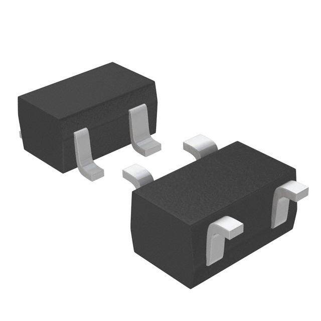
| 产品图片 |
|
| 产品型号 | TPS3839G33DQNR |
| PCN组件/产地 | |
| PCN设计/规格 | |
| rohs | 无铅 / 符合限制有害物质指令(RoHS)规范要求 |
| 产品系列 | - |
| 供应商器件封装 | 4-X2SON (1x1) |
| 其它名称 | 296-35532-2 |
| 包装 | 带卷 (TR) |
| 受监控电压数 | 1 |
| 复位 | 低有效 |
| 复位超时 | 最小为 120 ms |
| 安装类型 | 表面贴装 |
| 封装/外壳 | 4-XDFN 裸露焊盘 |
| 工作温度 | -40°C ~ 85°C |
| 标准包装 | 3,000 |
| 电压-阈值 | 3.08V |
| 类型 | 简单复位/加电复位 |
| 输出 | 推挽式,图腾柱 |


- 商务部:美国ITC正式对集成电路等产品启动337调查
- 曝三星4nm工艺存在良率问题 高通将骁龙8 Gen1或转产台积电
- 太阳诱电将投资9.5亿元在常州建新厂生产MLCC 预计2023年完工
- 英特尔发布欧洲新工厂建设计划 深化IDM 2.0 战略
- 台积电先进制程称霸业界 有大客户加持明年业绩稳了
- 达到5530亿美元!SIA预计今年全球半导体销售额将创下新高
- 英特尔拟将自动驾驶子公司Mobileye上市 估值或超500亿美元
- 三星加码芯片和SET,合并消费电子和移动部门,撤换高东真等 CEO
- 三星电子宣布重大人事变动 还合并消费电子和移动部门
- 海关总署:前11个月进口集成电路产品价值2.52万亿元 增长14.8%


PDF Datasheet 数据手册内容提取
Product Sample & Technical Tools & Support & Folder Buy Documents Software Community TPS3831,TPS3839 SBVS193D–JUNE2012–REVISEDJULY2015 TPS383x 150-nA, Ultralow Power, Supply Voltage Monitor 1 Features 3 Description • UltralowSupplyCurrent:150nA(Typical) The TPS3831 and TPS3839 devices (both referred to 1 as TPS383x) are ultralow current (150 nA, typical), • OperatingSupplyVoltage:0.9Vto6.5V voltage supervisory circuits that monitor a single • ValidResetforVDD>0.6V voltage. Both devices initiate an active-low reset • Push-PullRESETOutput signal whenever the VDD supply voltage drops below the factory-trimmed reset threshold voltage. The reset • Factory-TrimmedResetThresholdVoltages output remains low for 200 ms (typical) after the V DD • TemperatureRange:–40°Cto85°C voltage rises above the threshold voltage and • Packages:1-mm×1-mmX2SONor3-PinSOT23 hysteresis. These devices are designed to ignore fast transients on the VDD pin. The TPS3831 device 2 Applications includes a manual reset input that forces RESET low whenMRislow. • PortableandBattery-PoweredEquipment The ultralow current consumption of 150 nA makes • Metering these voltage supervisors ideal for use in low-power • IndustrialEquipment and portable applications. The TPS383x devices are • CellPhones specified to have the correct output logic state for supplyvoltagesdownto0.6V. • GlucoseMonitors • Tablets The TPS383x devices feature precision factory- trimmed threshold voltages and extremely low-power • Wearables operation. The TPS3831 device is available in a 4- pin, 1-mm × 1-mm (DQN) X2SON package. The TPS3839 device is available in a 3-pin SOT23 (DBZ) package or a 4-pin, 1-mm × 1-mm (DQN) X2SON package. DeviceInformation(1) PACKAGESIZE PARTNUMBER PACKAGE (NOM) TPS3831 X2SON(4) 1.00mmx1.00mm SOT-23(3) 2.92mmx2.37mm TPS3839 X2SON(4) 1.00mmx1.00mm (1) For all available packages, see the orderable addendum at theendofthedatasheet. TypicalApplicationCircuit SupplyCurrentvsTemperature 3.3 V 200 190 VDD = 1.2 V C1 180 VVDDDD == 35..30 VV 0.1mF A) 170 VDD = 6.5 V n VDD nt ( 160 e TPS383xK33 Microprocessor urr 150 C y 140 MR RESET RST ppl u 130 S TPS3831 GND 120 Only 110 100 −40 −15 10 35 60 85 Temperature (°C) G001 1 An IMPORTANT NOTICE at the end of this data sheet addresses availability, warranty, changes, use in safety-critical applications, intellectualpropertymattersandotherimportantdisclaimers.PRODUCTIONDATA.
TPS3831,TPS3839 SBVS193D–JUNE2012–REVISEDJULY2015 www.ti.com Table of Contents 1 Features.................................................................. 1 8.4 DeviceFunctionalModes........................................12 2 Applications........................................................... 1 9 ApplicationsandImplementation...................... 13 3 Description............................................................. 1 9.1 ApplicationInformation............................................13 4 RevisionHistory..................................................... 2 9.2 TypicalApplication..................................................13 5 DeviceOptions....................................................... 4 10 PowerSupplyRecommendations..................... 15 6 PinConfigurationandFunctions......................... 5 11 Layout................................................................... 15 11.1 LayoutGuidelines.................................................15 7 Specifications......................................................... 6 11.2 LayoutExample....................................................15 7.1 AbsoluteMaximumRatings......................................6 12 DeviceandDocumentationSupport................. 16 7.2 ESDRatings..............................................................6 7.3 RecommendedOperatingConditions.......................6 12.1 DeviceSupport......................................................16 7.4 ThermalInformation..................................................6 12.2 DocumentationSupport........................................16 7.5 ElectricalCharacteristics...........................................7 12.3 RelatedLinks........................................................16 7.6 TimingRequirements................................................8 12.4 CommunityResources..........................................16 7.7 TypicalCharacteristics..............................................9 12.5 Trademarks...........................................................16 12.6 ElectrostaticDischargeCaution............................16 8 DetailedDescription............................................ 11 12.7 Glossary................................................................17 8.1 Overview.................................................................11 13 Mechanical,Packaging,andOrderable 8.2 FunctionalBlockDiagram.......................................11 Information........................................................... 17 8.3 FeatureDescription.................................................11 4 Revision History NOTE:Pagenumbersforpreviousrevisionsmaydifferfrompagenumbersinthecurrentversion. ChangesfromRevisionC(February2015)toRevisionD Page • ChangedµAtonAindocumenttitle....................................................................................................................................... 1 • AddedTPS3839G25todocument......................................................................................................................................... 1 • ChangedApplicationssection:movedMeteringbullettosecondinlist,changedTabletsbullet,addedWearablesbullet..1 • ChangedfirstparagraphofDescriptionsection .................................................................................................................... 1 • ChangedDeviceInformationtable:changedPackageSizecolumnheadingandvalueofSOT-23row ............................. 1 • AddedTPS3839G25rowtoDeviceOptionstable ................................................................................................................ 4 • ChangedThermalInformationtable ...................................................................................................................................... 6 • ChangedV andV parametersinElectricalCharacteristicstable:changedtestconditions,addedTPS3839G25rows 7 IT– hys ChangesfromRevisionB(April2013)toRevisionC Page • AddedESDRatingstable,FeatureDescriptionsection,DeviceFunctionalModes,ApplicationandImplementation section,PowerSupplyRecommendationssection,Layoutsection,DeviceandDocumentationSupportsection,and Mechanical,Packaging,andOrderableInformationsection ................................................................................................. 1 • Changedtitleofdatasheet ................................................................................................................................................... 1 • ChangedOperatingSupplyVoltagebulletfrom0.6Vto0.9V.............................................................................................. 1 • ChangedlastsentenceofDescriptionsection ...................................................................................................................... 1 • Changedfrontpagefigure ..................................................................................................................................................... 1 • AddedMRparametertoAbsoluteMaximumRatings ........................................................................................................... 6 • ChangedconditionstatementforElectricalCharacteristics .................................................................................................. 7 • ChangedV parametersymboltoV ............................................................................................................................. 7 (VO) POR • ChangedFigure1................................................................................................................................................................... 8 • ChangedFunctionalBlockDiagram;addedhysteresissymboltoopamp.......................................................................... 11 • DeletedTypicalApplicationCircuitfigure............................................................................................................................. 13 2 SubmitDocumentationFeedback Copyright©2012–2015,TexasInstrumentsIncorporated
TPS3831,TPS3839 www.ti.com SBVS193D–JUNE2012–REVISEDJULY2015 ChangesfromRevisionA(September2012)toRevisionB Page • ChangedV testconditionsforhigh-leveloutputvoltageparameter................................................................................... 7 DD ChangesfromOriginal(June2012)toRevisionA Page • Changeddatasheetstatusfromproductpreviewtoproductiondata.................................................................................... 1 Copyright©2012–2015,TexasInstrumentsIncorporated SubmitDocumentationFeedback 3
TPS3831,TPS3839 SBVS193D–JUNE2012–REVISEDJULY2015 www.ti.com 5 Device Options THRESHOLD PACKAGE PRODUCT VOLTAGE(V) PACKAGE-LEAD DESIGNATOR(1) TPS3831A09 0.9 X2SON-4 DQN TPS3831G12 1.1 X2SON-4 DQN TPS3831E16 1.52 X2SON-4 DQN TPS3831G18 1.67 X2SON-4 DQN TPS3831L30 2.63 X2SON-4 DQN TPS3831K33 2.93 X2SON-4 DQN TPS3831G33 3.08 X2SON-4 DQN TPS3831K50 4.38 X2SON-4 DQN SOT23-3 DBZ TPS3839A09 0.9 X2SON-4 DQN SOT23-3 DBZ TPS3839G12 1.1 X2SON-4 DQN SOT23-3 DBZ TPS3839E16 1.52 X2SON-4 DQN SOT23-3 DBZ TPS3839G18 1.67 X2SON-4 DQN TPS3839G25 2.325 SOT23-3 DBZ SOT23-3 DBZ TPS3839L30 2.63 X2SON-4 DQN SOT23-3 DBZ TPS3839K33 2.93 X2SON-4 DQN SOT23-3 DBZ TPS3839G33 3.08 X2SON-4 DQN SOT23-3 DBZ TPS3839K50 4.38 X2SON-4 DQN (1) ForthemostcurrentpackageandorderinginformationseethePackageOptionAddendumattheendofthisdocument,orvisitthe deviceproductfolderatwww.ti.com. 4 SubmitDocumentationFeedback Copyright©2012–2015,TexasInstrumentsIncorporated
TPS3831,TPS3839 www.ti.com SBVS193D–JUNE2012–REVISEDJULY2015 6 Pin Configuration and Functions TPS3831DQNPackage 1-mm×1-mmX2SON TPS3839DQNPackage TopView 1-mm×1-mmX2SON TopView RESET 1 4 VDD RESET 1 4 VDD Thermal Pad Thermal Pad MR 2 3 GND NC 2 3 GND TPS3839DBZPackage SOT23-3 TopView GND 1 3 VDD RESET 2 PinFunctions PIN NO. I/O DESCRIPTION NAME TPS3839 TPS3839 TPS3831 (SOT23-3) (X2SON) (X2SON) GND 1 3 3 — Ground Manualreset.PullthispintoalogiclowtoasserttheRESEToutput. MR N/A N/A 2 I AftertheMRpinisdeasserted,theRESEToutputdeassertsafterthe resetdelay(t )elapses. d NC N/A 2 N/A — Nointernalconnection. Active-lowresetoutput.RESEThasapush-pulloutputdriveandis capableofdirectlydrivinginputpins.RESETislowaslongasV RESET 2 1 1 O DD remainsbelowthefactorythresholdvoltage,anduntilthedelaytime (t )elapsesafterV risesabovethethresholdvoltage. d DD Connecttogroundortoafloatingcopperplaneformechanical Thermalpad N/A Available Available — stability. VDD 3 4 4 I Supplyvoltage Copyright©2012–2015,TexasInstrumentsIncorporated SubmitDocumentationFeedback 5
TPS3831,TPS3839 SBVS193D–JUNE2012–REVISEDJULY2015 www.ti.com 7 Specifications 7.1 Absolute Maximum Ratings overoperatingfree-airtemperaturerange,unlessotherwisenoted(1) MIN MAX UNIT VDD,RESET –0.3 7 V Voltage MR –0.3 V +0.3 V DD Current RESETpin –10 10 mA Operatingambient,T –40 85 Temperature(2) A °C Storage,T –65 150 stg (1) StressesbeyondthoselistedunderAbsoluteMaximumRatingsmaycausepermanentdamagetothedevice.Thesearestressratings only,andfunctionaloperationofthedeviceattheseoranyotherconditionsbeyondthoseindicatedunderRecommendedOperating Conditionsisnotimplied.Exposuretoabsolute-maximum-ratedconditionsforextendedperiodsmayaffectdevicereliability. (2) Asaresultofthelowdissipatedpowerinthisdevice,thejunctiontemperatureisassumedtobeequaltotheambienttemperature. 7.2 ESD Ratings VALUE UNIT Humanbodymodel(HBM),perANSI/ESDA/JEDECJS-001(1) ±2000 V Electrostaticdischarge V (ESD) Chargeddevicemodel(CDM),perJEDECspecificationJESD22-C101(2) ±500 (1) JEDECdocumentJEP155statesthat500-VHBMallowssafemanufacturingwithastandardESDcontrolprocess. (2) JEDECdocumentJEP157statesthat250-VCDMallowssafemanufacturingwithastandardESDcontrolprocess. 7.3 Recommended Operating Conditions overoperatingfree-airtemperaturerange(unlessotherwisenoted) MIN NOM MAX UNIT V Inputsupplyvoltage 0.9 6.5 V DD V Manualresetpinvoltage 0 V V MR DD V RESETpinvoltage 0 6.5 V RESET I RESETpincurrent 0 8 mA RESET 7.4 Thermal Information TPS3831, TPS3839 TPS3839 THERMALMETRIC(1) UNIT DBZ(SOT23-3) DQN(X2SON) 3PINS 4PINS R Junction-to-ambientthermalresistance 346.6 216.1 °C/W θJA R Junction-to-case(top)thermalresistance 124.4 161.7 °C/W θJC(top) R Junction-to-boardthermalresistance 78.9 162.1 °C/W θJB ψ Junction-to-topcharacterizationparameter 11.5 5.1 °C/W JT ψ Junction-to-boardcharacterizationparameter 77.3 161.7 °C/W JB R Junction-to-case(bottom)thermalresistance N/A 123.0 °C/W θJC(bot) (1) Formoreinformationabouttraditionalandnewthermalmetrics,seetheSemiconductorandICPackageThermalMetricsapplication report,SPRA953. 6 SubmitDocumentationFeedback Copyright©2012–2015,TexasInstrumentsIncorporated
TPS3831,TPS3839 www.ti.com SBVS193D–JUNE2012–REVISEDJULY2015 7.5 Electrical Characteristics AtT =–40°Cto85°C,0.9V<V <6.5V,andC1=0.1µF,unlessotherwisenoted.Typicalvaluesareat25°C. A DD PARAMETER TESTCONDITIONS MIN TYP MAX UNIT V Inputsupplyvoltage 0.9 6.5 V DD V MinimumV voltageforvalidoutput I =1µA 0.6 V (POR) DD OL I Supplycurrent(intoVDDpin) Outputnotconnected 150 500 nA DD V =0.9Vto1.2V,I =120µA 0.4 DD OL V Low-leveloutputvoltage(RESETpin) V =1.2Vto2.8V,I =0.5mA 0.4 V OL DD OL V =2.8Vto6.5V,I =2mA 0.4 DD OL V =0.9Vto1.2V,I =–50µA V –0.4 DD OH DD V High-leveloutputvoltage(RESETpin) V =1.2Vto3.3V,I =–0.5mA V –0.4 V OH DD OH DD V =3.3Vto6.5V,I =–2mA V –0.4 DD OH DD V Low-levelinputvoltage(MRpin) 0.3V V IL DD V High-levelinputvoltage(MRpin) 0.7V V IH DD R MRpinpullupresistance 10 20 30 kΩ MR Negative-goinginputthresholdaccuracy T =25°C ±1% A TPS383xA09 0.874 0.9 0.914 TPS383xG12 1.073 1.1 1.117 TPS383xE16 1.482 1.52 1.543 TPS383xG18 1.628 1.67 1.695 V Negative-goingthresholdvoltage TPS3839G25 2.267 2.325 2.360 V IT– TPS383xL30 2.564 2.63 2.669 TPS383xK33 2.857 2.93 2.974 TPS383xG33 3.003 3.08 3.126 TPS383xK50 4.271 4.38 4.446 TPS383xA09 54 TPS383xG12 11 TPS383xE16 15 TPS383xG18 17 V Hysteresisvoltage TPS383xL30 26 mV hys TPS3839G25 23 TPS383xK33 29 TPS383xG33 31 TPS383xK50 44 Copyright©2012–2015,TexasInstrumentsIncorporated SubmitDocumentationFeedback 7
TPS3831,TPS3839 SBVS193D–JUNE2012–REVISEDJULY2015 www.ti.com 7.6 Timing Requirements AtT =–40°Cto85°C,0.9V<V <6.5V,andC1=0.1µF,unlessotherwisenoted.Typicalvaluesareat25°C. A DD MIN TYP MAX UNIT t RESETdelaytime(power-updelay) 120 200 350 ms d t Propagationdelay,V falling(power-downdelay) 20 µs PD_VDD DD t PropagationdelayfromMRlowtoRESETlow 46 ns PD_MR VDD VIT-+VHYS VIT- 0.6V MR 0.7V DD 0.3V DD t =ResetDelay d td td td =UndefinedState RESET Time Figure1. MRandVDDResetTiming 8 SubmitDocumentationFeedback Copyright©2012–2015,TexasInstrumentsIncorporated
TPS3831,TPS3839 www.ti.com SBVS193D–JUNE2012–REVISEDJULY2015 7.7 Typical Characteristics AtT =25°CandC =0.1µF,unlessotherwisenoted. A 1 200 220 190 VDD = 1.2 V TPS3839K33 VDD = 3.3 V A) 117800 VVDDDD == 56..05 VV ms) 210 nt (n 160 me ( Supply Curre 111345000 Reset Delay Ti 129000 120 110 100 180 −40 −15 10 35 60 85 −40 −15 10 35 60 85 Temperature (°C) Temperature (°C) G001 G002 Figure2.SupplyCurrentvsTemperature Figure3.ResetDelayvsTemperature 0.2 1.8 VDD = 1.8 V 0 1.6 %) V (IT–−0.2 V) 1.4 ge in −0.4 V (OH 1.2 n a −0.6 Ch TA = −40(cid:176)C −0.8 TPS3839A09 1 TTAA == 0+(cid:176)2C5(cid:176)C TPS3839K50 TA = +85(cid:176)C −1 0.8 −40 −15 10 35 60 85 0 0.5 1 1.5 2 2.5 3 3.5 Temperature (°C) G003 IOH (mA) G004 Figure4.ThresholdVoltagevsTemperature Figure5.V vsI andTemperatureforV =1.8V OH OH DD 3.5 4 VDD = 3.3 V VDD =4.0 V 3.5 2.5 V) V) (H (H 3 O O V V 1.5 TA = −40(cid:176)C 2.5 TA = −40(cid:176)C TA = 0(cid:176)C TA = 0(cid:176)C TA = +25(cid:176)C TA = +25(cid:176)C TA = +85(cid:176)C TA = +85(cid:176)C 0.5 2 0 2 4 6 8 10 0 2 4 6 8 10 12 IOH (mA) G005 IOH (mA) G006 Figure6.V vsI andTemperatureforV =3.3V Figure7.V vsI andTemperatureforV =4.0V OH OH DD OH OH DD Copyright©2012–2015,TexasInstrumentsIncorporated SubmitDocumentationFeedback 9
TPS3831,TPS3839 SBVS193D–JUNE2012–REVISEDJULY2015 www.ti.com Typical Characteristics (continued) AtT =25°CandC =0.1µF,unlessotherwisenoted. A 1 1.6 1.6 TA = −40(cid:176)C TA = −40(cid:176)C 1.4 TA = 0(cid:176)C 1.4 TA = 0(cid:176)C TA = +25(cid:176)C TA = +25(cid:176)C 1.2 TA = +25(cid:176)C 1.2 TA = +85(cid:176)C 1 1 V) V) (OL 0.8 (OL 0.8 V V 0.6 0.6 0.4 0.4 0.2 0.2 VDD = 1.8 V VDD = 3.3 V 0 0 0 1 2 3 4 5 0 2 4 6 8 10 IOL (mA) G007 IOL (mA) G008 Figure8.V vsI andTemperatureforV =1.8V Figure9.V vsI andTemperatureforV =3.3V OL OL DD OL OL DD 1.4 s) 50 1.2 TTTAAA === −0+(cid:176)42C05(cid:176)(cid:176)CC Reset (µ 45 Reset Occurs Above Line 1 TA = +85(cid:176)C er 40 g g Tri 35 V) 0.8 n (OL atio 30 V 0.6 ur D 25 e 0.4 uls 20 P 0.2 um 15 VDD = 4.0 V nim 0 Mi 10 0 2 4 6 8 10 0 5 10 15 20 25 30 35 IOL (mA) G009 VDD voltage drop below VIT− (%) G010 Figure10.V vsI andTemperatureforV =4.0V Figure11.MaximumPulseDurationvsPercentof OL OL DD ThresholdOverdrive 10 SubmitDocumentationFeedback Copyright©2012–2015,TexasInstrumentsIncorporated
TPS3831,TPS3839 www.ti.com SBVS193D–JUNE2012–REVISEDJULY2015 8 Detailed Description 8.1 Overview TheTPS3831andTPS3839areultralowcurrentvoltagesupervisorycircuitsthatmonitortheinputsupplyvoltage of these devices. Both devices assert an active-low reset whenever the V supply voltage drops below the DD negative-going threshold voltage (V ). The output, RESET, remains asserted for approximately IT– 200 ms after the V voltage rises above the positive-going threshold voltage (V + V ). These devices are DD IT– hys designedtoignorefasttransientsontheVDDpin. TheTPS3831deviceincludesamanualresetinput(MR)thatcanbeusedtoforcetheRESETsignallow,evenif thesupplyvoltageisaboveV . IT– 8.2 Functional Block Diagram VDD Delay RESET V REF GND VDD MR (TPS3831Only) 8.3 Feature Description 8.3.1 VDDTransientRejection The TPS383x (TPS3831 and TPS3839) devices have built-in rejection of fast transients on the VDD pin. Transientrejectiondependsonboththedurationandamplitudeofthetransient.Transientamplitudeismeasured fromthebottomofthetransienttothenegativethresholdvoltage(V )ofthedevice,asshowninFigure12. IT– V DD VIT- Transient Amplitude Transient Duration (t ) W Figure12. VoltageTransientMeasurement Copyright©2012–2015,TexasInstrumentsIncorporated SubmitDocumentationFeedback 11
TPS3831,TPS3839 SBVS193D–JUNE2012–REVISEDJULY2015 www.ti.com Feature Description (continued) Figure 13 shows the relationship between the transient amplitude and duration required to trigger a reset. Any combinationofdurationandamplitudegreaterthanthatshowninFigure13 generatesaresetsignal. s) 50 µ set ( 45 Reset Occurs Above Line e R er 40 g g Tri 35 n atio 30 ur D 25 e s ul 20 P m u 15 m ni Mi 10 0 5 10 15 20 25 30 35 VDD voltage drop below VIT− (%) G010 Figure13. TPS3839TransientRejection 8.3.2 ManualReset(MR)Input(TPS3831Only) Themanualreset(MR)inputallowsaprocessor,orotherlogicdevices,toinitiateareset(TPS3831deviceonly). A logic low (0.3 V ) on MR causes RESET to assert. After MR returns to a logic high and V is greater than DD DD the threshold voltage, RESET is deasserted after the reset delay time, t , elapses. MR is internally tied to VDD d with a 20-kΩ resistor; therefore, this pin can be left unconnected if MR is not used. If a logic signal driving MR doesnotgofullytoV ,someadditionalcurrentdrawsintoVDDasaresultoftheinternalpullupresistoron MR. DD Tominimizecurrentdraw,alogic-levelFETcanbeused,asshowninFigure14. VDD 20 kW MR TPS3831 GND Figure14. UsingaLogic-LevelFETtoMinimizeCurrentDraw 8.4 Device Functional Modes 8.4.1 NormalOperation(V >V ) DD DD(min) When the voltage on VDD is greater than V , the RESET output corresponds to the voltage on the VDD pin DD(min) relativetoV . IT– 8.4.2 BelowV (V <V <V DD(min) (POR) DD DD(min) When the voltage on VDD is less than V but greater than the power-on reset voltage (V ), the RESET DD(min) (POR) outputisasserted. 8.4.3 BelowPower-OnReset(V <V DD (POR) When the voltage on VDD is lower than the power-on reset voltage (V ), the RESET output is undefined. Do (POR) notrelyontheRESEToutputforproperdevicefunctionunderthiscondition. 12 SubmitDocumentationFeedback Copyright©2012–2015,TexasInstrumentsIncorporated
TPS3831,TPS3839 www.ti.com SBVS193D–JUNE2012–REVISEDJULY2015 9 Applications and Implementation NOTE Information in the following applications sections is not part of the TI component specification, and TI does not warrant its accuracy or completeness. TI’s customers are responsible for determining suitability of components for their purposes. Customers should validateandtesttheirdesignimplementationtoconfirmsystemfunctionality. 9.1 Application Information Low operating voltage and threshold options make the TPS383x devices well-suited for monitoring single-cell, alkaline-batteryapplications. 9.2 Typical Application Figure 15 shows the TPS3839A09 used to disable a boost converter when the cell voltage reaches 0.9 V, which is the end of the discharge voltage for a single alkaline battery cell. When the cell voltage reaches 0.9 V, the TPS61261 enable pin is driven low. This setting disables the TPS61261 and places it in a low-current shutdown state. The combination of the TPS3839 and TPS61261 devices consumes only 250 nA (typical) from the dischargedbattery. VIN VOUT 3.3 V at 40 mA 4.7 PH L FB 10 PF 10 PF VDD TPS61261 One-Cell TPS3839A09 Alkaline RESET EN RI GND 5 k: GND Figure15. DisabledBoostConverter 9.2.1 DesignRequirements Table1liststhedesignrequirementsforFigure15. Table1.DesignRequirementsandResults DESIGNRESULT DESIGNREQUIREMENTS TPS3839A09 TPS61261 COMBINED Inputvoltagerangeof0.9Vto1.7V 0.9Vto6.5V 0.8Vto4V 0.9Vto4V Shutdowncurrent<3µA 0.5μA(maximum) 1.5μA(maximum) 2.0μA(maximum) Outputvoltageof3.3V N/A 3.3V 3.3V Outputcurrentof50mA N/A 100mA 100mA Switchingfrequency≥1MHz N/A 2.5MHz 2.5MHz Copyright©2012–2015,TexasInstrumentsIncorporated SubmitDocumentationFeedback 13
TPS3831,TPS3839 SBVS193D–JUNE2012–REVISEDJULY2015 www.ti.com 9.2.2 DetailedDesignProcedure 9.2.2.1 InputCapacitor The TPS383x devices use a unique sampling scheme to maintain an extremely low average quiescent current of 150 nA. The TPS383x devices typically consume only approximately 100 nA of dc current. However, this current rises to approximately 15 µA for about 200 µs when the TPS383x devices sample the input voltage. If the source impedance back to the supply voltage is high, then the additional current during sampling may trigger a false reset as a result of the apparent voltage drop at VDD. For applications with high-impedance input supplies (including trace impedance), TI recommends adding a small 0.1-µF bypass capacitor near the TPS3839 VDD pin. This bypass capacitor effectively keeps the average current at 150 nA and reduces the effects of a high- impedancevoltagesource. 9.2.2.2 BidirectionalResetPins Some devices have bidirectional reset pins that act both as an input and an output. For applications where the TPS383x devices drive a bidirectional reset pin, place a series resistor between the TPS383x output and the reset pin to protect against excessive current flow when both the TPS383x devices and the reset pin attempt to drive the reset line. Figure 16 shows the connection of the TPS3839K33 to a bidirectional reset pin of a microcontrollerusingaseriesresistor. 3.3 V V VDD CC Microprocessor TPS3839K33 47 k: RST RESET GND Figure16. ConnectiontoaBidirectionalResetPin 9.2.3 ApplicationCurve 200 190 VDD = 1.2 V VDD = 3.3 V 180 VDD = 5.0 V A) 170 VDD = 6.5 V n nt ( 160 e urr 150 C y 140 pl p u 130 S 120 110 100 −40 −15 10 35 60 85 Temperature (°C) G001 Figure17. SupplyCurrentvsTemperature 14 SubmitDocumentationFeedback Copyright©2012–2015,TexasInstrumentsIncorporated
TPS3831,TPS3839 www.ti.com SBVS193D–JUNE2012–REVISEDJULY2015 10 Power Supply Recommendations These devices are designed to operate from an input supply with a voltage range between 0.9 V and 6.5 V. Use a low-impedance power supply to eliminate inaccuracies caused by the extra current during the input-voltage samplingdiscussedintheInputCapacitorsection. 11 Layout 11.1 Layout Guidelines Make sure the connection to the VDD pin is low impedance and able to carry 15 µA without a significant voltage drop. Place a 0.1-µF bypass capacitor near the VDD pin if the 15-µA sampling current causes too much voltage droop. 11.2 Layout Example 1 CVDD 3 RESET 2 Flag Input Supply Figure18. RecommendedLayout Copyright©2012–2015,TexasInstrumentsIncorporated SubmitDocumentationFeedback 15
TPS3831,TPS3839 SBVS193D–JUNE2012–REVISEDJULY2015 www.ti.com 12 Device and Documentation Support 12.1 Device Support 12.1.1 DevelopmentSupport 12.1.1.1 EvaluationModules Two evaluation modules (EVMs) are available to assist in the initial circuit performance evaluation using the TPS3831 and TPS3839. The TPS3831G33EVM-187 and TPS3839K33EVM-112 evaluation modules (and related user's guides) can be requested at the TI website through the product folders or purchased directly from theTIeStore. 12.1.1.2 SpiceModels Computer simulation of circuit performance using SPICE is often useful when analyzing the performance of analog circuits and systems. SPICE models for the TPS3831 and TPS3839 devices are available through each oftheproductfoldersunderTools& Software. 12.2 Documentation Support 12.2.1 RelatedDocumentation • TPS3831G33EVM-187User'sGuide,SLVU774 • TPS3839K33EVM-112User'sGuide,SLVU758. • TPS61261DataSheet,SLVSA99 12.3 Related Links Table 2 lists quick access links. Categories include technical documents, support and community resources, toolsandsoftware,andquickaccesstosampleorbuy. Table2.RelatedLinks TECHNICAL TOOLS& SUPPORT& PARTS PRODUCTFOLDER SAMPLE&BUY DOCUMENTS SOFTWARE COMMUNITY TPS3831 Clickhere Clickhere Clickhere Clickhere Clickhere TPS3839 Clickhere Clickhere Clickhere Clickhere Clickhere 12.4 Community Resources The following links connect to TI community resources. Linked contents are provided "AS IS" by the respective contributors. They do not constitute TI specifications and do not necessarily reflect TI's views; see TI's Terms of Use. TIE2E™OnlineCommunity TI'sEngineer-to-Engineer(E2E)Community.Createdtofostercollaboration amongengineers.Ate2e.ti.com,youcanaskquestions,shareknowledge,exploreideasandhelp solveproblemswithfellowengineers. DesignSupport TI'sDesignSupport QuicklyfindhelpfulE2Eforumsalongwithdesignsupporttoolsand contactinformationfortechnicalsupport. 12.5 Trademarks E2EisatrademarkofTexasInstruments. Allothertrademarksarethepropertyoftheirrespectiveowners. 12.6 Electrostatic Discharge Caution Thesedeviceshavelimitedbuilt-inESDprotection.Theleadsshouldbeshortedtogetherorthedeviceplacedinconductivefoam duringstorageorhandlingtopreventelectrostaticdamagetotheMOSgates. 16 SubmitDocumentationFeedback Copyright©2012–2015,TexasInstrumentsIncorporated
TPS3831,TPS3839 www.ti.com SBVS193D–JUNE2012–REVISEDJULY2015 12.7 Glossary SLYZ022—TIGlossary. Thisglossarylistsandexplainsterms,acronyms,anddefinitions. 13 Mechanical, Packaging, and Orderable Information The following pages include mechanical, packaging, and orderable information. This information is the most current data available for the designated devices. This data is subject to change without notice and revision of thisdocument.Forbrowser-basedversionsofthisdatasheet,refertotheleft-handnavigation. Copyright©2012–2015,TexasInstrumentsIncorporated SubmitDocumentationFeedback 17
PACKAGE OPTION ADDENDUM www.ti.com 6-Feb-2020 PACKAGING INFORMATION Orderable Device Status Package Type Package Pins Package Eco Plan Lead/Ball Finish MSL Peak Temp Op Temp (°C) Device Marking Samples (1) Drawing Qty (2) (6) (3) (4/5) TPS3831A09DQNR ACTIVE X2SON DQN 4 3000 Green (RoHS NIPDAU Level-1-260C-UNLIM -40 to 85 A3 & no Sb/Br) TPS3831A09DQNT ACTIVE X2SON DQN 4 250 Green (RoHS NIPDAU Level-1-260C-UNLIM -40 to 85 A3 & no Sb/Br) TPS3831E16DQNR ACTIVE X2SON DQN 4 3000 Green (RoHS NIPDAU Level-1-260C-UNLIM -40 to 85 A5 & no Sb/Br) TPS3831E16DQNT ACTIVE X2SON DQN 4 250 Green (RoHS NIPDAU Level-1-260C-UNLIM -40 to 85 A5 & no Sb/Br) TPS3831G12DQNR ACTIVE X2SON DQN 4 3000 Green (RoHS NIPDAU Level-1-260C-UNLIM -40 to 85 A4 & no Sb/Br) TPS3831G12DQNT ACTIVE X2SON DQN 4 250 Green (RoHS NIPDAU Level-1-260C-UNLIM -40 to 85 A4 & no Sb/Br) TPS3831G18DQNR ACTIVE X2SON DQN 4 3000 Green (RoHS NIPDAU Level-1-260C-UNLIM -40 to 85 A6 & no Sb/Br) TPS3831G18DQNT ACTIVE X2SON DQN 4 250 Green (RoHS NIPDAU Level-1-260C-UNLIM -40 to 85 A6 & no Sb/Br) TPS3831G33DQNR ACTIVE X2SON DQN 4 3000 Green (RoHS NIPDAU Level-1-260C-UNLIM -40 to 85 A7 & no Sb/Br) TPS3831G33DQNT ACTIVE X2SON DQN 4 250 Green (RoHS NIPDAU Level-1-260C-UNLIM -40 to 85 A7 & no Sb/Br) TPS3831K33DQNR ACTIVE X2SON DQN 4 3000 Green (RoHS NIPDAU Level-1-260C-UNLIM -40 to 85 A8 & no Sb/Br) TPS3831K33DQNT ACTIVE X2SON DQN 4 250 Green (RoHS NIPDAU Level-1-260C-UNLIM -40 to 85 A8 & no Sb/Br) TPS3831K50DQNR ACTIVE X2SON DQN 4 3000 Green (RoHS NIPDAU Level-1-260C-UNLIM -40 to 85 A9 & no Sb/Br) TPS3831K50DQNT ACTIVE X2SON DQN 4 250 Green (RoHS NIPDAU Level-1-260C-UNLIM -40 to 85 A9 & no Sb/Br) TPS3831L30DQNR ACTIVE X2SON DQN 4 3000 Green (RoHS NIPDAU Level-1-260C-UNLIM -40 to 85 BA & no Sb/Br) TPS3831L30DQNT ACTIVE X2SON DQN 4 250 Green (RoHS NIPDAU Level-1-260C-UNLIM -40 to 85 BA & no Sb/Br) TPS3839A09DBZR ACTIVE SOT-23 DBZ 3 3000 Green (RoHS NIPDAUAG Level-1-260C-UNLIM -40 to 85 PZDI & no Sb/Br) Addendum-Page 1
PACKAGE OPTION ADDENDUM www.ti.com 6-Feb-2020 Orderable Device Status Package Type Package Pins Package Eco Plan Lead/Ball Finish MSL Peak Temp Op Temp (°C) Device Marking Samples (1) Drawing Qty (2) (6) (3) (4/5) TPS3839A09DBZT ACTIVE SOT-23 DBZ 3 250 Green (RoHS NIPDAUAG Level-1-260C-UNLIM -40 to 85 PZDI & no Sb/Br) TPS3839A09DQNR ACTIVE X2SON DQN 4 3000 Green (RoHS NIPDAU Level-1-260C-UNLIM -40 to 85 ZJ & no Sb/Br) TPS3839A09DQNT ACTIVE X2SON DQN 4 250 Green (RoHS NIPDAU Level-1-260C-UNLIM -40 to 85 ZJ & no Sb/Br) TPS3839E16DBZR ACTIVE SOT-23 DBZ 3 3000 Green (RoHS NIPDAUAG Level-1-260C-UNLIM -40 to 85 PZCI & no Sb/Br) TPS3839E16DBZT ACTIVE SOT-23 DBZ 3 250 Green (RoHS NIPDAUAG Level-1-260C-UNLIM -40 to 85 PZCI & no Sb/Br) TPS3839E16DQNR ACTIVE X2SON DQN 4 3000 Green (RoHS NIPDAU Level-1-260C-UNLIM -40 to 85 ZK & no Sb/Br) TPS3839E16DQNT ACTIVE X2SON DQN 4 250 Green (RoHS NIPDAU Level-1-260C-UNLIM -40 to 85 ZK & no Sb/Br) TPS3839G12DBZR ACTIVE SOT-23 DBZ 3 3000 Green (RoHS NIPDAUAG Level-1-260C-UNLIM -40 to 85 PZBI & no Sb/Br) TPS3839G12DBZT ACTIVE SOT-23 DBZ 3 250 Green (RoHS NIPDAUAG Level-1-260C-UNLIM -40 to 85 PZBI & no Sb/Br) TPS3839G12DQNR ACTIVE X2SON DQN 4 3000 Green (RoHS NIPDAU Level-1-260C-UNLIM -40 to 85 ZE & no Sb/Br) TPS3839G12DQNT ACTIVE X2SON DQN 4 250 Green (RoHS NIPDAU Level-1-260C-UNLIM -40 to 85 ZE & no Sb/Br) TPS3839G18DBZR ACTIVE SOT-23 DBZ 3 3000 Green (RoHS NIPDAUAG Level-1-260C-UNLIM -40 to 85 PZAI & no Sb/Br) TPS3839G18DBZT ACTIVE SOT-23 DBZ 3 250 Green (RoHS NIPDAUAG Level-1-260C-UNLIM -40 to 85 PZAI & no Sb/Br) TPS3839G18DQNR ACTIVE X2SON DQN 4 3000 Green (RoHS NIPDAU Level-1-260C-UNLIM -40 to 85 ZL & no Sb/Br) TPS3839G18DQNT ACTIVE X2SON DQN 4 250 Green (RoHS NIPDAU Level-1-260C-UNLIM -40 to 85 ZL & no Sb/Br) TPS3839G25DBZR ACTIVE SOT-23 DBZ 3 3000 Green (RoHS NIPDAU Level-1-260C-UNLIM -40 to 85 PZNI & no Sb/Br) TPS3839G25DBZT ACTIVE SOT-23 DBZ 3 250 Green (RoHS NIPDAU Level-1-260C-UNLIM -40 to 85 PZNI & no Sb/Br) TPS3839G33DBZR ACTIVE SOT-23 DBZ 3 3000 Green (RoHS NIPDAUAG Level-1-260C-UNLIM -40 to 85 PYZI & no Sb/Br) Addendum-Page 2
PACKAGE OPTION ADDENDUM www.ti.com 6-Feb-2020 Orderable Device Status Package Type Package Pins Package Eco Plan Lead/Ball Finish MSL Peak Temp Op Temp (°C) Device Marking Samples (1) Drawing Qty (2) (6) (3) (4/5) TPS3839G33DBZT ACTIVE SOT-23 DBZ 3 250 Green (RoHS NIPDAUAG Level-1-260C-UNLIM -40 to 85 PYZI & no Sb/Br) TPS3839G33DQNR ACTIVE X2SON DQN 4 3000 Green (RoHS NIPDAU Level-1-260C-UNLIM -40 to 85 ZG & no Sb/Br) TPS3839G33DQNT ACTIVE X2SON DQN 4 250 Green (RoHS NIPDAU Level-1-260C-UNLIM -40 to 85 ZG & no Sb/Br) TPS3839K33DBZR ACTIVE SOT-23 DBZ 3 3000 Green (RoHS NIPDAUAG Level-1-260C-UNLIM -40 to 85 PYYI & no Sb/Br) TPS3839K33DBZT ACTIVE SOT-23 DBZ 3 250 Green (RoHS NIPDAUAG Level-1-260C-UNLIM -40 to 85 PYYI & no Sb/Br) TPS3839K33DQNR ACTIVE X2SON DQN 4 3000 Green (RoHS NIPDAU Level-1-260C-UNLIM -40 to 85 ZF & no Sb/Br) TPS3839K33DQNT ACTIVE X2SON DQN 4 250 Green (RoHS NIPDAU Level-1-260C-UNLIM -40 to 85 ZF & no Sb/Br) TPS3839K50DBZR ACTIVE SOT-23 DBZ 3 3000 Green (RoHS NIPDAUAG Level-1-260C-UNLIM -40 to 85 PYXI & no Sb/Br) TPS3839K50DBZT ACTIVE SOT-23 DBZ 3 250 Green (RoHS NIPDAUAG Level-1-260C-UNLIM -40 to 85 PYXI & no Sb/Br) TPS3839K50DQNR ACTIVE X2SON DQN 4 3000 Green (RoHS NIPDAU Level-1-260C-UNLIM -40 to 85 ZH & no Sb/Br) TPS3839K50DQNT ACTIVE X2SON DQN 4 250 Green (RoHS NIPDAU Level-1-260C-UNLIM -40 to 85 ZH & no Sb/Br) TPS3839L30DBZR ACTIVE SOT-23 DBZ 3 3000 Green (RoHS NIPDAUAG Level-1-260C-UNLIM -40 to 85 PYWI & no Sb/Br) TPS3839L30DBZT ACTIVE SOT-23 DBZ 3 250 Green (RoHS NIPDAUAG Level-1-260C-UNLIM -40 to 85 PYWI & no Sb/Br) TPS3839L30DQNR ACTIVE X2SON DQN 4 3000 Green (RoHS NIPDAU Level-1-260C-UNLIM -40 to 85 ZI & no Sb/Br) TPS3839L30DQNT ACTIVE X2SON DQN 4 250 Green (RoHS NIPDAU Level-1-260C-UNLIM -40 to 85 ZI & no Sb/Br) (1) The marketing status values are defined as follows: ACTIVE: Product device recommended for new designs. LIFEBUY: TI has announced that the device will be discontinued, and a lifetime-buy period is in effect. NRND: Not recommended for new designs. Device is in production to support existing customers, but TI does not recommend using this part in a new design. PREVIEW: Device has been announced but is not in production. Samples may or may not be available. OBSOLETE: TI has discontinued the production of the device. Addendum-Page 3
PACKAGE OPTION ADDENDUM www.ti.com 6-Feb-2020 (2) RoHS: TI defines "RoHS" to mean semiconductor products that are compliant with the current EU RoHS requirements for all 10 RoHS substances, including the requirement that RoHS substance do not exceed 0.1% by weight in homogeneous materials. Where designed to be soldered at high temperatures, "RoHS" products are suitable for use in specified lead-free processes. TI may reference these types of products as "Pb-Free". RoHS Exempt: TI defines "RoHS Exempt" to mean products that contain lead but are compliant with EU RoHS pursuant to a specific EU RoHS exemption. Green: TI defines "Green" to mean the content of Chlorine (Cl) and Bromine (Br) based flame retardants meet JS709B low halogen requirements of <=1000ppm threshold. Antimony trioxide based flame retardants must also meet the <=1000ppm threshold requirement. (3) MSL, Peak Temp. - The Moisture Sensitivity Level rating according to the JEDEC industry standard classifications, and peak solder temperature. (4) There may be additional marking, which relates to the logo, the lot trace code information, or the environmental category on the device. (5) Multiple Device Markings will be inside parentheses. Only one Device Marking contained in parentheses and separated by a "~" will appear on a device. If a line is indented then it is a continuation of the previous line and the two combined represent the entire Device Marking for that device. (6) Lead/Ball Finish - Orderable Devices may have multiple material finish options. Finish options are separated by a vertical ruled line. Lead/Ball Finish values may wrap to two lines if the finish value exceeds the maximum column width. Important Information and Disclaimer:The information provided on this page represents TI's knowledge and belief as of the date that it is provided. TI bases its knowledge and belief on information provided by third parties, and makes no representation or warranty as to the accuracy of such information. Efforts are underway to better integrate information from third parties. TI has taken and continues to take reasonable steps to provide representative and accurate information but may not have conducted destructive testing or chemical analysis on incoming materials and chemicals. TI and TI suppliers consider certain information to be proprietary, and thus CAS numbers and other limited information may not be available for release. In no event shall TI's liability arising out of such information exceed the total purchase price of the TI part(s) at issue in this document sold by TI to Customer on an annual basis. Addendum-Page 4
PACKAGE MATERIALS INFORMATION www.ti.com 16-May-2019 TAPE AND REEL INFORMATION *Alldimensionsarenominal Device Package Package Pins SPQ Reel Reel A0 B0 K0 P1 W Pin1 Type Drawing Diameter Width (mm) (mm) (mm) (mm) (mm) Quadrant (mm) W1(mm) TPS3831A09DQNR X2SON DQN 4 3000 180.0 9.5 1.16 1.16 0.5 4.0 8.0 Q2 TPS3831A09DQNT X2SON DQN 4 250 180.0 9.5 1.16 1.16 0.5 4.0 8.0 Q2 TPS3831E16DQNR X2SON DQN 4 3000 180.0 9.5 1.16 1.16 0.5 4.0 8.0 Q2 TPS3831E16DQNT X2SON DQN 4 250 180.0 9.5 1.16 1.16 0.5 4.0 8.0 Q2 TPS3831G12DQNR X2SON DQN 4 3000 180.0 9.5 1.16 1.16 0.5 4.0 8.0 Q2 TPS3831G12DQNT X2SON DQN 4 250 180.0 9.5 1.16 1.16 0.5 4.0 8.0 Q2 TPS3831G18DQNR X2SON DQN 4 3000 180.0 9.5 1.16 1.16 0.5 4.0 8.0 Q2 TPS3831G18DQNT X2SON DQN 4 250 180.0 9.5 1.16 1.16 0.5 4.0 8.0 Q2 TPS3831G33DQNR X2SON DQN 4 3000 180.0 9.5 1.16 1.16 0.5 4.0 8.0 Q2 TPS3831G33DQNT X2SON DQN 4 250 180.0 9.5 1.16 1.16 0.5 4.0 8.0 Q2 TPS3831K33DQNR X2SON DQN 4 3000 180.0 9.5 1.16 1.16 0.5 4.0 8.0 Q2 TPS3831K33DQNT X2SON DQN 4 250 180.0 9.5 1.16 1.16 0.5 4.0 8.0 Q2 TPS3831K50DQNR X2SON DQN 4 3000 180.0 9.5 1.16 1.16 0.5 4.0 8.0 Q2 TPS3831K50DQNT X2SON DQN 4 250 180.0 9.5 1.16 1.16 0.5 4.0 8.0 Q2 TPS3831L30DQNR X2SON DQN 4 3000 180.0 9.5 1.16 1.16 0.5 4.0 8.0 Q2 TPS3831L30DQNT X2SON DQN 4 250 180.0 9.5 1.16 1.16 0.5 4.0 8.0 Q2 TPS3839A09DBZR SOT-23 DBZ 3 3000 179.0 8.4 3.15 2.95 1.22 4.0 8.0 Q3 TPS3839A09DBZT SOT-23 DBZ 3 250 179.0 8.4 3.15 2.95 1.22 4.0 8.0 Q3 PackMaterials-Page1
PACKAGE MATERIALS INFORMATION www.ti.com 16-May-2019 Device Package Package Pins SPQ Reel Reel A0 B0 K0 P1 W Pin1 Type Drawing Diameter Width (mm) (mm) (mm) (mm) (mm) Quadrant (mm) W1(mm) TPS3839A09DQNR X2SON DQN 4 3000 180.0 9.5 1.16 1.16 0.5 4.0 8.0 Q2 TPS3839A09DQNT X2SON DQN 4 250 180.0 9.5 1.16 1.16 0.5 4.0 8.0 Q2 TPS3839E16DBZR SOT-23 DBZ 3 3000 179.0 8.4 3.15 2.95 1.22 4.0 8.0 Q3 TPS3839E16DBZT SOT-23 DBZ 3 250 179.0 8.4 3.15 2.95 1.22 4.0 8.0 Q3 TPS3839E16DQNR X2SON DQN 4 3000 180.0 9.5 1.16 1.16 0.5 4.0 8.0 Q2 TPS3839E16DQNT X2SON DQN 4 250 180.0 9.5 1.16 1.16 0.5 4.0 8.0 Q2 TPS3839G12DBZR SOT-23 DBZ 3 3000 179.0 8.4 3.15 2.95 1.22 4.0 8.0 Q3 TPS3839G12DBZT SOT-23 DBZ 3 250 179.0 8.4 3.15 2.95 1.22 4.0 8.0 Q3 TPS3839G12DQNR X2SON DQN 4 3000 180.0 9.5 1.16 1.16 0.5 4.0 8.0 Q2 TPS3839G12DQNT X2SON DQN 4 250 180.0 9.5 1.16 1.16 0.5 4.0 8.0 Q2 TPS3839G18DBZR SOT-23 DBZ 3 3000 179.0 8.4 3.15 2.95 1.22 4.0 8.0 Q3 TPS3839G18DBZT SOT-23 DBZ 3 250 179.0 8.4 3.15 2.95 1.22 4.0 8.0 Q3 TPS3839G18DQNR X2SON DQN 4 3000 180.0 9.5 1.16 1.16 0.5 4.0 8.0 Q2 TPS3839G18DQNT X2SON DQN 4 250 180.0 9.5 1.16 1.16 0.5 4.0 8.0 Q2 TPS3839G25DBZR SOT-23 DBZ 3 3000 179.0 8.4 3.15 2.95 1.22 4.0 8.0 Q3 TPS3839G25DBZT SOT-23 DBZ 3 250 179.0 8.4 3.15 2.95 1.22 4.0 8.0 Q3 TPS3839G33DBZR SOT-23 DBZ 3 3000 179.0 8.4 3.15 2.95 1.22 4.0 8.0 Q3 TPS3839G33DBZT SOT-23 DBZ 3 250 179.0 8.4 3.15 2.95 1.22 4.0 8.0 Q3 TPS3839G33DQNR X2SON DQN 4 3000 180.0 9.5 1.16 1.16 0.5 4.0 8.0 Q2 TPS3839G33DQNT X2SON DQN 4 250 180.0 9.5 1.16 1.16 0.5 4.0 8.0 Q2 TPS3839K33DBZR SOT-23 DBZ 3 3000 179.0 8.4 3.15 2.95 1.22 4.0 8.0 Q3 TPS3839K33DBZT SOT-23 DBZ 3 250 179.0 8.4 3.15 2.95 1.22 4.0 8.0 Q3 TPS3839K33DQNR X2SON DQN 4 3000 180.0 9.5 1.16 1.16 0.5 4.0 8.0 Q2 TPS3839K33DQNT X2SON DQN 4 250 180.0 9.5 1.16 1.16 0.5 4.0 8.0 Q2 TPS3839K50DBZR SOT-23 DBZ 3 3000 179.0 8.4 3.15 2.95 1.22 4.0 8.0 Q3 TPS3839K50DBZT SOT-23 DBZ 3 250 179.0 8.4 3.15 2.95 1.22 4.0 8.0 Q3 TPS3839K50DQNR X2SON DQN 4 3000 180.0 9.5 1.16 1.16 0.5 4.0 8.0 Q2 TPS3839K50DQNT X2SON DQN 4 250 180.0 9.5 1.16 1.16 0.5 4.0 8.0 Q2 TPS3839L30DBZR SOT-23 DBZ 3 3000 179.0 8.4 3.15 2.95 1.22 4.0 8.0 Q3 TPS3839L30DBZT SOT-23 DBZ 3 250 179.0 8.4 3.15 2.95 1.22 4.0 8.0 Q3 TPS3839L30DQNR X2SON DQN 4 3000 180.0 9.5 1.16 1.16 0.5 4.0 8.0 Q2 TPS3839L30DQNT X2SON DQN 4 250 180.0 9.5 1.16 1.16 0.5 4.0 8.0 Q2 PackMaterials-Page2
PACKAGE MATERIALS INFORMATION www.ti.com 16-May-2019 *Alldimensionsarenominal Device PackageType PackageDrawing Pins SPQ Length(mm) Width(mm) Height(mm) TPS3831A09DQNR X2SON DQN 4 3000 184.0 184.0 19.0 TPS3831A09DQNT X2SON DQN 4 250 184.0 184.0 19.0 TPS3831E16DQNR X2SON DQN 4 3000 184.0 184.0 19.0 TPS3831E16DQNT X2SON DQN 4 250 184.0 184.0 19.0 TPS3831G12DQNR X2SON DQN 4 3000 184.0 184.0 19.0 TPS3831G12DQNT X2SON DQN 4 250 184.0 184.0 19.0 TPS3831G18DQNR X2SON DQN 4 3000 184.0 184.0 19.0 TPS3831G18DQNT X2SON DQN 4 250 184.0 184.0 19.0 TPS3831G33DQNR X2SON DQN 4 3000 184.0 184.0 19.0 TPS3831G33DQNT X2SON DQN 4 250 184.0 184.0 19.0 TPS3831K33DQNR X2SON DQN 4 3000 184.0 184.0 19.0 TPS3831K33DQNT X2SON DQN 4 250 184.0 184.0 19.0 TPS3831K50DQNR X2SON DQN 4 3000 184.0 184.0 19.0 TPS3831K50DQNT X2SON DQN 4 250 184.0 184.0 19.0 TPS3831L30DQNR X2SON DQN 4 3000 184.0 184.0 19.0 TPS3831L30DQNT X2SON DQN 4 250 184.0 184.0 19.0 TPS3839A09DBZR SOT-23 DBZ 3 3000 203.0 203.0 35.0 TPS3839A09DBZT SOT-23 DBZ 3 250 203.0 203.0 35.0 TPS3839A09DQNR X2SON DQN 4 3000 184.0 184.0 19.0 TPS3839A09DQNT X2SON DQN 4 250 184.0 184.0 19.0 PackMaterials-Page3
PACKAGE MATERIALS INFORMATION www.ti.com 16-May-2019 Device PackageType PackageDrawing Pins SPQ Length(mm) Width(mm) Height(mm) TPS3839E16DBZR SOT-23 DBZ 3 3000 203.0 203.0 35.0 TPS3839E16DBZT SOT-23 DBZ 3 250 203.0 203.0 35.0 TPS3839E16DQNR X2SON DQN 4 3000 184.0 184.0 19.0 TPS3839E16DQNT X2SON DQN 4 250 184.0 184.0 19.0 TPS3839G12DBZR SOT-23 DBZ 3 3000 203.0 203.0 35.0 TPS3839G12DBZT SOT-23 DBZ 3 250 203.0 203.0 35.0 TPS3839G12DQNR X2SON DQN 4 3000 184.0 184.0 19.0 TPS3839G12DQNT X2SON DQN 4 250 184.0 184.0 19.0 TPS3839G18DBZR SOT-23 DBZ 3 3000 203.0 203.0 35.0 TPS3839G18DBZT SOT-23 DBZ 3 250 203.0 203.0 35.0 TPS3839G18DQNR X2SON DQN 4 3000 184.0 184.0 19.0 TPS3839G18DQNT X2SON DQN 4 250 184.0 184.0 19.0 TPS3839G25DBZR SOT-23 DBZ 3 3000 203.0 203.0 35.0 TPS3839G25DBZT SOT-23 DBZ 3 250 203.0 203.0 35.0 TPS3839G33DBZR SOT-23 DBZ 3 3000 203.0 203.0 35.0 TPS3839G33DBZT SOT-23 DBZ 3 250 203.0 203.0 35.0 TPS3839G33DQNR X2SON DQN 4 3000 184.0 184.0 19.0 TPS3839G33DQNT X2SON DQN 4 250 184.0 184.0 19.0 TPS3839K33DBZR SOT-23 DBZ 3 3000 203.0 203.0 35.0 TPS3839K33DBZT SOT-23 DBZ 3 250 203.0 203.0 35.0 TPS3839K33DQNR X2SON DQN 4 3000 184.0 184.0 19.0 TPS3839K33DQNT X2SON DQN 4 250 184.0 184.0 19.0 TPS3839K50DBZR SOT-23 DBZ 3 3000 203.0 203.0 35.0 TPS3839K50DBZT SOT-23 DBZ 3 250 203.0 203.0 35.0 TPS3839K50DQNR X2SON DQN 4 3000 184.0 184.0 19.0 TPS3839K50DQNT X2SON DQN 4 250 184.0 184.0 19.0 TPS3839L30DBZR SOT-23 DBZ 3 3000 203.0 203.0 35.0 TPS3839L30DBZT SOT-23 DBZ 3 250 203.0 203.0 35.0 TPS3839L30DQNR X2SON DQN 4 3000 184.0 184.0 19.0 TPS3839L30DQNT X2SON DQN 4 250 184.0 184.0 19.0 PackMaterials-Page4
4203227/C
PACKAGE OUTLINE DBZ0003A SOT-23 - 1.12 mm max height SCALE 4.000 SMALL OUTLINE TRANSISTOR 2.64 C 2.10 1.12 MAX 1.4 1.2 B A 0.1 C PIN 1 INDEX AREA 1 0.95 3.04 1.9 2.80 3 2 0.5 3X 0.3 0.10 0.2 C A B (0.95) TYP 0.01 0.25 GAGE PLANE 0.20 TYP 0.08 0.6 TYP 0 -8 TYP 0.2 SEATING PLANE 4214838/C 04/2017 NOTES: 1. All linear dimensions are in millimeters. Any dimensions in parenthesis are for reference only. Dimensioning and tolerancing per ASME Y14.5M. 2. This drawing is subject to change without notice. 3. Reference JEDEC registration TO-236, except minimum foot length. www.ti.com
EXAMPLE BOARD LAYOUT DBZ0003A SOT-23 - 1.12 mm max height SMALL OUTLINE TRANSISTOR PKG 3X (1.3) 1 3X (0.6) SYMM 3 2X (0.95) 2 (R0.05) TYP (2.1) LAND PATTERN EXAMPLE SCALE:15X SOLDER MASK SOLDER MASK METAL UNDER METAL OPENING OPENING SOLDER MASK 0.07 MAX 0.07 MIN ALL AROUND ALL AROUND NON SOLDER MASK SOLDER MASK DEFINED DEFINED (PREFERRED) SOLDER MASK DETAILS 4214838/C 04/2017 NOTES: (continued) 4. Publication IPC-7351 may have alternate designs. 5. Solder mask tolerances between and around signal pads can vary based on board fabrication site. www.ti.com
EXAMPLE STENCIL DESIGN DBZ0003A SOT-23 - 1.12 mm max height SMALL OUTLINE TRANSISTOR PKG 3X (1.3) 1 3X (0.6) SYMM 3 2X(0.95) 2 (R0.05) TYP (2.1) SOLDER PASTE EXAMPLE BASED ON 0.125 THICK STENCIL SCALE:15X 4214838/C 04/2017 NOTES: (continued) 6. Laser cutting apertures with trapezoidal walls and rounded corners may offer better paste release. IPC-7525 may have alternate design recommendations. 7. Board assembly site may have different recommendations for stencil design. www.ti.com
None
PACKAGE OUTLINE DQN0004A X2SON - 0.4 mm max height PLASTIC SMALL OUTLINE - NO LEAD B 1.05 A 0.95 1 1.05 PIN 1 0.95 INDEX AREA C 0.4 MAX SEATING PLANE 0.08 NOTE 6 0.48+0.12 0.05 (0.05) TYP -0.1 0.00 2 NOTE 6 3 EXPOSED 5 THERMAL PAD 2X 0.65 (0.07) TYP NOTE 5 1 4 PIN 1 ID 4X 0.28 0.15 (OPTIONAL) (0.11) NOTE 4 0.3 0.1 C A B 0.2 0.05 C 3X 0.30 0.15 4215302/E 12/2016 NOTES: 1. All linear dimensions are in millimeters. Any dimensions in parenthesis are for reference only. Dimensioning and tolerancing per ASME Y14.5M. 2. This drawing is subject to change without notice. 3. The package thermal pad must be soldered to the printed circuit board for optimal thermal and mechanical performance. 4. Features may not exist. Recommend use of pin 1 marking on top of package for orientation purposes. 5. Shape of exposed side leads may differ. 6. Number and location of exposed tie bars may vary. www.ti.com
EXAMPLE BOARD LAYOUT DQN0004A X2SON - 0.4 mm max height PLASTIC SMALL OUTLINE - NO LEAD (0.86) SYMM 4X (0.36) 4X SEE DETAIL (0.03) 4 4X (0.21) 1 SYMM 5 (0.65) 4X (0.18) 2 3 ( 0.48) (0.22) TYP EXPOSED METAL CLEARANCE LAND PATTERN EXAMPLE SCALE: 40X 0.05 MIN ALL AROUND SOLDER MASK EXPOSED METAL OPENING METAL UNDER SOLDER MASK SOLDER MASK DEFINED SOLDER MASK DETAIL 4215302/E 12/2016 NOTES: (continued) 7. This package is designed to be soldered to a thermal pad on the board. For more information, see Texas Instruments literature number SLUA271 (www.ti.com/lit/slua271). 8. If any vias are implemented, it is recommended that vias under paste be filled, plugged or tented. www.ti.com
EXAMPLE STENCIL DESIGN DQN0004A X2SON - 0.4 mm max height PLASTIC SMALL OUTLINE - NO LEAD (0.9) SYMM 4X (0.4) 4X (0.03) 4 1 4X (0.21) 5 SYMM (0.65) SOLDER MASK 4X (0.22) EDGE 2 3 ( 0.45) 4X (0.235) SOLDER PASTE EXAMPLE BASED ON 0.075 - 0.1mm THICK STENCIL EXPOSED PAD 88% PRINTED SOLDER COVERAGE BY AREA SCALE: 60X 4215302/E 12/2016 NOTES: (continued) 9. Laser cutting apertures with trapezoidal walls and rounded corners may offer better paste release. IPC-7525 may have alternate design recommendations. www.ti.com
IMPORTANTNOTICEANDDISCLAIMER TI PROVIDES TECHNICAL AND RELIABILITY DATA (INCLUDING DATASHEETS), DESIGN RESOURCES (INCLUDING REFERENCE DESIGNS), APPLICATION OR OTHER DESIGN ADVICE, WEB TOOLS, SAFETY INFORMATION, AND OTHER RESOURCES “AS IS” AND WITH ALL FAULTS, AND DISCLAIMS ALL WARRANTIES, EXPRESS AND IMPLIED, INCLUDING WITHOUT LIMITATION ANY IMPLIED WARRANTIES OF MERCHANTABILITY, FITNESS FOR A PARTICULAR PURPOSE OR NON-INFRINGEMENT OF THIRD PARTY INTELLECTUAL PROPERTY RIGHTS. These resources are intended for skilled developers designing with TI products. You are solely responsible for (1) selecting the appropriate TI products for your application, (2) designing, validating and testing your application, and (3) ensuring your application meets applicable standards, and any other safety, security, or other requirements. These resources are subject to change without notice. TI grants you permission to use these resources only for development of an application that uses the TI products described in the resource. Other reproduction and display of these resources is prohibited. No license is granted to any other TI intellectual property right or to any third party intellectual property right. TI disclaims responsibility for, and you will fully indemnify TI and its representatives against, any claims, damages, costs, losses, and liabilities arising out of your use of these resources. TI’s products are provided subject to TI’s Terms of Sale (www.ti.com/legal/termsofsale.html) or other applicable terms available either on ti.com or provided in conjunction with such TI products. TI’s provision of these resources does not expand or otherwise alter TI’s applicable warranties or warranty disclaimers for TI products. Mailing Address: Texas Instruments, Post Office Box 655303, Dallas, Texas 75265 Copyright © 2020, Texas Instruments Incorporated