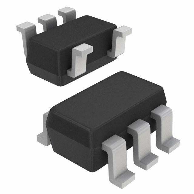
ICGOO在线商城 > 集成电路(IC) > PMIC - 监控器 > MAX802TCSA+
- 型号: MAX802TCSA+
- 制造商: Maxim
- 库位|库存: xxxx|xxxx
- 要求:
| 数量阶梯 | 香港交货 | 国内含税 |
| +xxxx | $xxxx | ¥xxxx |
查看当月历史价格
查看今年历史价格
MAX802TCSA+产品简介:
ICGOO电子元器件商城为您提供MAX802TCSA+由Maxim设计生产,在icgoo商城现货销售,并且可以通过原厂、代理商等渠道进行代购。 MAX802TCSA+价格参考。MaximMAX802TCSA+封装/规格:PMIC - 监控器, 推挽式,图腾柱 监控器 1 通道 8-SOIC。您可以下载MAX802TCSA+参考资料、Datasheet数据手册功能说明书,资料中有MAX802TCSA+ 详细功能的应用电路图电压和使用方法及教程。
Maxim Integrated的MAX802TCSA+是一款电源管理集成电路(PMIC),具体功能为电压监控器。该芯片主要用于监测系统中的电源电压,确保其稳定在安全范围内,适用于对电源稳定性要求较高的电子设备。

典型应用场景包括:

1. 嵌入式系统:用于监控微控制器或处理器的供电电压,防止电压过低导致系统异常或数据丢失;
2. 工业控制设备:在PLC、工控机等设备中监测电源状态,保障工业系统稳定运行;
3. 通信设备:用于基站、路由器或交换机中,监控电源电压以确保通信连续性;
4. 消费电子产品:如智能家电、安防设备中,用于实现电源管理与故障保护;
5. 电池供电系统:便携设备或备用电源系统中,监测电池电压并提供低电压警告或复位信号。

该器件具有低功耗、高精度、响应速度快等优点,适合用于多种电源监控需求,提升系统可靠性与安全性。
| 参数 | 数值 |
| 产品目录 | 集成电路 (IC)半导体 |
| 描述 | IC SUPERVISOR MPU 8-SOIC监控电路 3/3.3V MPU Supervisor |
| 产品分类 | |
| 品牌 | Maxim Integrated |
| 产品手册 | |
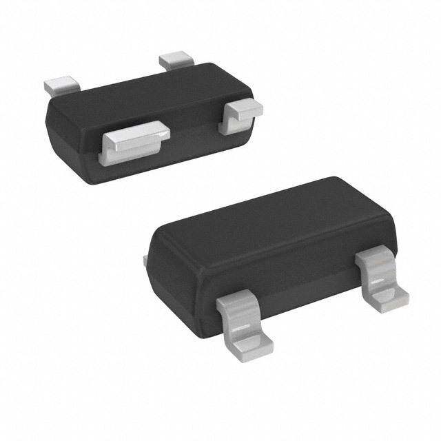
| 产品图片 |
|
| rohs | 符合RoHS无铅 / 符合限制有害物质指令(RoHS)规范要求 |
| 产品系列 | 电源管理 IC,监控电路,Maxim Integrated MAX802TCSA+- |
| NumberofInputsMonitored | 1 Input |
| 数据手册 | |
| 产品型号 | MAX802TCSA+ |
| 产品培训模块 | http://www.digikey.cn/PTM/IndividualPTM.page?site=cn&lang=zhs&ptm=25703http://www.digikey.cn/PTM/IndividualPTM.page?site=cn&lang=zhs&ptm=25705 |
| 产品种类 | 监控电路 |
| 人工复位 | No Manual Reset |
| 供应商器件封装 | 8-SOIC N |
| 功率失效检测 | Yes |
| 包装 | 管件 |
| 受监控电压数 | 1 |
| 商标 | Maxim Integrated |
| 复位 | 低有效 |
| 复位超时 | 最小为 140 ms |
| 安装类型 | 表面贴装 |
| 安装风格 | SMD/SMT |
| 封装 | Tube |
| 封装/外壳 | 8-SOIC(0.154",3.90mm 宽) |
| 封装/箱体 | SOIC-8 |
| 工作温度 | 0°C ~ 70°C |
| 工作电源电流 | 50 uA |
| 工厂包装数量 | 100 |
| 最大功率耗散 | 471 mW |
| 最大工作温度 | + 70 C |
| 最小工作温度 | 0 C |
| 标准包装 | 1 |
| 欠电压阈值 | 3 V |
| 电压-阈值 | 3.075V |
| 电池备用开关 | Backup |
| 电源电压-最大 | 5.5 V |
| 电源电压-最小 | 1 V |
| 监视器 | Watchdog |
| 类型 | Voltage Supervisory |
| 系列 | MAX802T |
| 芯片启用信号 | No Chip Enable |
| 被监测输入数 | 1 Input |
| 输出 | 推挽式,图腾柱 |
| 输出类型 | Active Low, Push-Pull |
| 过电压阈值 | 3.14 V |
| 重置延迟时间 | 200 ms |
| 阈值电压 | 3 V |
| 零件号别名 | MAX802T |




- 商务部:美国ITC正式对集成电路等产品启动337调查
- 曝三星4nm工艺存在良率问题 高通将骁龙8 Gen1或转产台积电
- 太阳诱电将投资9.5亿元在常州建新厂生产MLCC 预计2023年完工
- 英特尔发布欧洲新工厂建设计划 深化IDM 2.0 战略
- 台积电先进制程称霸业界 有大客户加持明年业绩稳了
- 达到5530亿美元!SIA预计今年全球半导体销售额将创下新高
- 英特尔拟将自动驾驶子公司Mobileye上市 估值或超500亿美元
- 三星加码芯片和SET,合并消费电子和移动部门,撤换高东真等 CEO
- 三星电子宣布重大人事变动 还合并消费电子和移动部门
- 海关总署:前11个月进口集成电路产品价值2.52万亿元 增长14.8%




PDF Datasheet 数据手册内容提取
MAX690T/S/R, MAX704T/S/R, 3.0V/3.3V Microprocessor MAX802T/S/R, MAX804‒MAX806T/S/R Supervisory Circuits General Description Features These microprocessor (µP) supervisory circuits reduce the ● RESET and RESET Outputs complexity and number of components required for pow- ● Manual Reset Input er-supply monitoring and battery-control functions in µP ● Precision Supply-Voltage Monitor systems. They significantly improve system reliability and ● 200ms Reset Time Delay accuracy compared to separate ICs or discrete components. ● Watchdog Timer (1.6sec timeout) These devices are designed for use in systems powered ● Battery-Backup Power Switching—Battery Can by 3.0V or 3.3V supplies. See the selector guide in the Exceed VCC in Normal Operation back of this data sheet for similar devices designed for ● 40µA VCC Supply Current 5V systems. The suffixes denote different reset threshold ● 1µA Battery Supply Current voltages: 3.075V (T), 2.925V (S), and 2.625V (R) (see the ● Voltage Monitor for Power-Fail or Low-Battery Reset Threshold section in the Detailed Description). All Warning these parts are available in 8-pin DIP and SO packages. ● Guaranteed RESET Assertion to VCC = 1V Functions offered in this series are as follows: ● 8-Pin DIP and SO Packages T Active-Low ReAscetti ve-High Res Wetatchdog Input ManuInapl Rutese tB ackuSpw-hiBtrceahsttheoryld AcPcouwraecry-FaCilo mpPaorwateorr-Fail Reset Window A●●●● pBEICpnamrtliettitbileccleiargadyle -dtµnPiePtood I w nPnCesosotrwrenuedtmrr oC eMlloneomtrsnspituotreinrsg and Controllers MAX690 ±4% ±75mV ● Portable Equipment MAX704 ±4% ±75mV MAX802 ±2% ±2% Ordering Information MAX804 ±2% ±2% PART** TEMP RANGE PIN-PACKAGE MAX805 ±4% ±75mV MAX690_CPA 0°C to +70°C 8 Plastic DIP MAX806 ±2% ±2% MAX690_CSA 0°C to +70°C 8 SO MAX690_C/D 0°C to +70°C Dice* Typical Operating Circuits MAX690_EPA -40°C to +85°C 8 Plastic DIP MAX690_ESA -40°C to +85°C 8 SO REGULATED +3.3V OR +3.0V UNREGULATED VCCµP MAX690_MJA -55°C to +125°C 8 CERDIP DC R1 0.1µF VCC (RREESSEETT) RESET Ordering Information continued at end of data sheet. MAX690T/S/RPFO NMI *Contact factory for dice specifications. PFI MMAAXX880024TT//SS//RRWDI I/O LINEGND **These parts offer a choice of reset threshold voltage. Select R2 LIT3H.6IVUM MAX805T/S/R BUS the letter corresponding to the desired nominal reset threshold BATTERY voltage (T = 3.075V, S = 2.925V, R = 2.625V) and insert it into VBATT VOUT GND VCC the blank to complete the part number. 0.1µF 0.1µF CMOS RAM Devices in PDIP and SO packages are available in both leaded GND and lead(Pb)-free packaging. Specify lead free by adding the + symbol at the end of the part number when ordering. Lead free ( ) ARE FOR MAX804T/S/R, MAX805T/S/R not available for CERDIP package. Typical Operating Circuits continued at at end of data Pin Configuration appears at end of data sheet. sheet. 19-0243; Rev 3; 4/15
MAX690T/S/R, MAX704T/S/R, 3.0V/3.3V Microprocessor MAX802T/S/R, MAX804−MAX806T/S/R Supervisory Circuits Absolute Maximum Ratings Terminal Voltage (with respect to GND) Continuous Power Dissipation (TA = +70°C) VCC ...................................................................-0.3V to +6.0V Plastic DIP (derate 9.09mW/°C above +70°C) ............727mW VBATT ..............................................................-0.3V to +6.0V SO (derate 5.88mW/°C above +70°C) ........................471mW All Other Inputs.................-0.3V to the higher of VCC or VBATT CERDIP (derate 8.00mW/°C above +70°C) ................640mW Continuous Input Current Operating Temperature Ranges VCC ...............................................................................100mA MAX690_C_ _/MAX704_C_ _/MAX80_ _C_ _ .......0°C to +70°C VBATT ............................................................................18mA MAX690_E_ _/MAX704_E_ _/MAX80_ _E_ _. ...-40°C to +85°C GND ................................................................................18mA MAX690_M_ _/MAX704_M_ _/MAX80_ _M_ _ ...-55°C to +125°C Output Current Storage Temperature Range ............................-65°C to +160°C RESET, PFO ..................................................................18mA Lead Temperature (soldering, 10s) .................................+300°C VOUT .............................................................................100mA Stresses beyond those listed under “Absolute Maximum Ratings” may cause permanent damage to the device. These are stress ratings only, and functional operation of the device at these or any other conditions beyond those indicated in the operational sections of the specifications is not implied. Exposure to absolute maximum rating conditions for extended periods may affect device reliability. Electrical Characteristics (VCC = 3.17V to 5.5V for the MAX690T/MAX704T/MAX80_T, VCC = 3.02V to 5.5V for the MAX690S/MAX704S/MAX80_S, VCC = 2.72V to 5.5V for the MAX690R/MAX704R/MAX80_R; VBATT = 3.6V; TA = TMIN to TMAX; unless otherwise noted. Typical values are at TA = +25°C.) PARAMETER SYMBOL CONDITIONS MIN TYP MAX UNITS Operating Voltage Range, MAX690_C, MAX704_C, MAX80_ _C 1.0 5.5 V VCC, VBATT (Note 1) MAX690_E/M, MAX704_E/M, MAX80_ _E/M 1.1 5.5 MAX690_C/E, MAX704_C/E, 40 50 MAX80_ _C/E, VCC < 3.6V MAX690_C/E, MAX704_C/E, 50 65 V(eCxCcl uSduipnpgl yIO CUuTr)rent ISUPPLY M(MRA X= 7V0C4C_/ MMAAXX8609_0 __MC,/ EM,A VXC7C0 4<_ 5M.5, V µA MAX806_) 40 55 MAX80_ _M, VCC < 3.6V MAX690_M, MAX704_M, 50 70 MAX80_ _M, VCC < 5.5V VBCacCk Supu pMpolyd Ce(uerxreclnutd iinn gB aIOttUeTry)- M(MRA X= 7V0C4C_/ VCC = 2.0V, VBATT = 2.3V 25 50 µA MAX806_) VBATT Supply Current, Any MAX690_C/E, MAX704_C/E, MAX80_ _C/E 0.4 1 µA Mode (excluding IOUT) (Note 2) MAX690_M, MAX704_M, MAX80_ _M 0.4 10 Battery Leakage Current MAX690_C/E, MAX704_C/E, MAX80_ _C/E 0.01 0.5 µA (Note 3) MAX690_M, MAX704_M, MAX80_ _M 0.01 5 MAX690_C/E, MAX704_C/E, MAX80_ _C/E, VCC VCC IOUT = 5mA (Note 4) -0.3 -0.015 MAX690_C/E, MAX704_C/E, MAX80_ _C/E VCC VCC IOUT = 50mA -0.3 -0.15 VOUT Output Voltage MIOAUXT 6=9 05_mMA, (MNAotXe7 40)4_M, MAX80_ _M -0V.C03C5 -0V.C01C5 V MAX690_M, MAX704_M, MAX80_ _M VCC VCC IOUT = 50mA -0.35 -0.15 IOUT = 250µA, VCC > 2.5V (Note 4) -0V.0C0C1 5 -0V.0C0C0 6 www.maximintegrated.com Maxim Integrated │ 2
MAX690T/S/R, MAX704T/S/R, 3.0V/3.3V Microprocessor MAX802T/S/R, MAX804−MAX806T/S/R Supervisory Circuits Electrical Characteristics (continued) (VCC = 3.17V to 5.5V for the MAX690T/MAX704T/MAX80_T, VCC = 3.02V to 5.5V for the MAX690S/MAX704S/MAX80_S, VCC = 2.72V to 5.5V for the MAX690R/MAX704R/MAX80_R; VBATT = 3.6V; TA = TMIN to TMAX; unless otherwise noted. Typical values are at TA = +25°C.) PARAMETER SYMBOL CONDITIONS MIN TYP MAX UNITS VBATT VBATT VOUT in Battery-Backup IOUT = 250µA, VBATT = 2.3V - 0.1 - 0.034 V Mode VBATT IOUT = 1mA, VBATT = 2.3V -0.14 Battery Switch Threshold, VBATT - VCC, VSW > VCC > 1.75V (Note 5) 65 25 mV VCC Falling VSW VBATT > VCC (Note 6) 2.30 2.40 2.50 V Battery Switch Threshold, This value is identical to the reset threshold, V VCC Rising (Note 7) VCC rising VCC falling 3.00 3.075 3.15 MAX690T/704T/805T VCC rising 3.00 3.085 3.17 VCC falling 3.00 3.075 3.12 MAX802T/804T/806T VCC rising 3.00 3.085 3.14 VCC falling 2.85 2.925 3.00 MAX690S/704S/805S VCC rising 2.85 2.935 3.02 Reset Threshold (Note 8) VRST V VCC falling 2.88 2.925 3.00 MAX802S/804S/806S VCC rising 2.88 2.935 3.02 VCC falling 2.55 2.625 2.70 MAX690R/704R/805R VCC rising 2.55 2.635 2.72 VCC falling 2.59 2.625 2.70 MAX802R/804R/806S VCC rising 2.59 2.635 2.72 Reset Timeout Period tWP VCC < 3.6V 140 200 280 ms PFO, RESET Output Voltage VOH ISOURCE = 50µA V0C.3C- V0C.0C5- V PFO, RESET Output Short to IOS VCC = 3.3V, VOH = 0V 180 500 µV GND Current (Note 4) PFO, RESET, RESET ISINK = 1.2mA; VOL MAX690_/704_/802_/806_, VCC = VRST min; 0.06 0.3 V Output Voltage MAX804_/805_, VCC = VRST max VBATT = 0V, VCC = 1.0V, ISINK = 40µA, 0.13 0.3 MAX690_C, MAX704_C, MAX80_ _C PFO, RESET Output Voltage VOL V VBATT = 0V, VCC = 1.2V, ISINK = 200µA, 0.17 0.3 MAX690_E/M, MAX704_E/M, MAX80_ _E/M MAX804_C, RESET Output Leakage VBATT = 0V, MAX805_C -1 +1 Current (Note 9) VVCRCES =E TV R=S 0TV m, VinC; C MAX804_E/M, -10 +10 µA MAX805_E/M www.maximintegrated.com Maxim Integrated │ 3
MAX690T/S/R, MAX704T/S/R, 3.0V/3.3V Microprocessor MAX802T/S/R, MAX804−MAX806T/S/R Supervisory Circuits Electrical Characteristics (continued) (VCC = 3.17V to 5.5V for the MAX690T/MAX704T/MAX80_T, VCC = 3.02V to 5.5V for the MAX690S/MAX704S/MAX80_S, VCC = 2.72V to 5.5V for the MAX690R/MAX704R/MAX80_R; VBATT = 3.6V; TA = TMIN to TMAX; unless otherwise noted. Typical values are at TA = +25C.) PARAMETER SYMBOL CONDITIONS MIN TYP MAX UNITS MAX802_C/E, MAX804_C/E, PFI Input Threshold VPFT VVCPFCI <fa 3lli.n6gV MAX806_C/E 1.212 1.237 1.262 V MAX690_/MAX704_/MAX805_ 1.187 1.237 1.287 MAX690_C/E, MAX704_C/E, MAX80_ _C/E -25 2 25 PFI Input Current nA MAX690_M, MAX704_M, MAX80_ _M -500 2 500 MAX690_C/E, MAX704_C/E, 10 20 MAX80_ _C/E PFI Hysteresis, PFI Rising VPFH VCC < 3.6V mV MAX690_M, MAX704_M, 10 25 MAX80_ _M MAX690_C/E, MAX704_C/E, MAX80_ _C/E -25 2 25 PFI Input Current nA MAX690_M, MAX704_M, MAX80_ _M -500 2 500 VIH 0.7 x VCC MR Input Threshold MAX704_/MAX806_ only V VIL 0.3 x VCC MR Pulse Width tMR MAX704_/MAX806_ only 100 20 ns MR to Reset Delay tMD MAX704_/MAX806_ only 60 500 ns MR Pull-Up Current MAX704_/MAX806_ only, MR = 0V, VCC = 3V 20 60 350 µA VIH 0.7 x VCC WDI Input Threshold MAX690_/MAX802_/MAX804_/MAX805_ only V VIL 0.3 x VCC MAX690_C/E, MAX802_C/E, -1 +0.01 +1 WDI Input Current 0V< VCC < MAX804_C/E, MAX805_C/E µA 5.5V MAX690_M, MAX802_M, -10 +0.01 +10 MAX804_M, MAX805_M MAX690/MAX802/MAX804/ Watchdog Timeout Period tWD VCC < 3.6V MAX805 only 1.12 1.60 2.24 s WDI Pulse Width MAX690_/MAX802_/MAX804_/MAX805_ only 100 20 ns Note 1: VCC supply current, logic input leakage, watchdog functionality (MAX690_/802_/805_/804_), MR functionality (MAX704_/806_), PFI functionality, state of RESET (MAX690_/704_/802_/806_), and RESET (MAX804_/805_) tested at VBATT = 3.6V, and VCC = 5.5V. The state of RESET or RESET and PFO is tested at VCC = VCC min. Note 2: Tested at VBATT = 3.6V, VCC = 3.5V and 0V. The battery current will rise to 10µA over a narrow transition window around VCC = 1.9V. Note 3: Leakage current into the battery is tested under the worst-case conditions at VCC = 5.5V, VBATT = 1.8V and at VCC = 1.5V, VBATT= 1.0V. Note 4: Guaranteed by design. Note 5: When VSW > VCC > VBATT, VOUT remains connected to VCC until VCC drops below VBATT. The VCC-to-VBATT compara- tor has a small 25mV typical hysteresis to prevent oscillation. For VCC < 1.75V (typ), VOUT switches to VBATT regardless of the voltage on VBATT. Note 6: When VBATT > VCC > VSW, VOUT remains connected to VCC until VCC drops below the battery switch threshold (VSW). Note 7: VOUT switches from VBATT to VCC when VCC rises above the reset threshold, independent of VBATT. Switchover back to VCC occurs at the exact voltage that causes RESET to go high (on the MAX804_/805_, RESET goes low); however switchover occurs 200ms prior to reset. Note 8: The reset threshold tolerance is wider for VCC rising than for VCC falling to accommodate the 10mV typical hysteresis, which prevents internal oscillation. Note 9: The leakage current into or out of the RESET pin is tested with RESET asserted (RESET output high impedance). www.maximintegrated.com Maxim Integrated │ 4
MAX690T/S/R, MAX704T/S/R, 3.0V/3.3V Microprocessor MAX802T/S/R, MAX804−MAX806T/S/R Supervisory Circuits Typical Operating Characteristics (TA = +25°C, unless otherwise noted.) VCC-TO-VOUT ON-RESISTANCE VBATT-TO-VOUT ON-RESISTANCE SUPPLY CURRENT vs. TEMPERATURE vs. TEMPERATURE vs. TEMPERATURE E (Ω) 54 VBATT = 3.0V MAX690 toc01 CE (Ω) 180 VCC = 0V VBATT = 2V MAX690 toc02 5405 VCC = 5V MAX690-806 TOC03 SISTANC 3 VCC = 2.5V VCC = 3.3V ESISTAN 140 VBATT = 3V ENT (µA) 40 ON-REOUT 2 V ON-ROUT 100 VBATT = 3.3V PLY CURR 35 VPBFIA =T TG N= D3V VCC = 3.3V V-TO-VCC 1 VCC = 5V VBATT-TO- 60 VBATT = 5V SUP 30 MR/WDI FLOATING VCC = 2.5V 0 20 25 –60–40 –20 0 20 40 60 80 100 120 140 –60–40 –20 0 20 40 60 80 100 120 140 –60–40 –20 0 20 40 60 80 100 120 140 TEMPERATURE (°C) TEMPERATURE (°C) TEMPERATURE (°C) BATTERY SUPPLY CURRENT RESET TIMEOUT PERIOD RESET-COMPARATOR PROPAGATION vs. TEMPERATURE vs. TEMPERATURE DELAY vs. TEMPERATURE CURRENT (nA)101,010000000 VPCFCI = = G 0NVD VBATT = 5V MAX690 toc04 PERIOD (ms)222110628 VCC = 5V MAX690 toc05 DELAY (µs) 322062 V10B0AmTVT O= V3E.0RVDRIVE MAX690 toc06 Y T VBATT = 3.0V N TTERY SUPPL 10 VBATT = 3V ESET TIMEOU204 PROPAGATIO 18 A 1 R200 14 B VBATT = 2V VCC = 3.3V 0.1 196 10 –60–40 –20 0 20 40 60 80 100 120 140 –60–40 –20 0 20 40 60 80 100 120 140 –60–40 –20 0 20 40 60 80 100 120 140 TEMPERATURE (°C) TEMPERATURE (°C) TEMPERATURE (°C) PFI THRESHOLD NORMALIZED RESET THRESHOLD vs. TEMPERATURE vs. TEMPERATURE 1.240 VCC = 3.3V MAX690 toc07 D (V) 1.004 MAX690 toc08 1.238 VCC = 5V HOL 1.002 D (V) RES OL 1.236 TH 1.000 H T S E RE VCC = 2.5V ES PFI TH 1.234 LIZED R 0.998 A 1.232 RM 0.996 O N VBATT = 3.0V VBATT = 3.0V 1.230 0.994 –60–40 –20 0 20 40 60 80 100 120 140 –60–40 –20 0 20 40 60 80 100 120 140 TEMPERATURE (°C) TEMPERATURE (°C) www.maximintegrated.com Maxim Integrated │ 5
MAX690T/S/R, MAX704T/S/R, 3.0V/3.3V Microprocessor MAX802T/S/R, MAX804−MAX806T/S/R Supervisory Circuits Pin Description PIN MAX690 MAX704 MAX804 NAME FUNCTION MAX802 MAX806 MAX805 Supply Output for CMOS RAM. When VCC is above the reset threshold, VOUT is 1 1 1 VOUT connected to VCC through a p-channel MOSFET switch. When VCC falls below VSW and VBATT, VBATT connects to VOUT. Connect to VCC if no battery is used. 2 2 2 VCC Main Supply Input 3 3 3 GND Ground 4 4 4 PFI Power-Fail Input. When PFI is less than VPFT or when VCC falls below VSW, PFO goes low; otherwise, PFO remains high. Connect to ground if unused. 5 5 5 PFO Power-Fail Output. When PFI is less than VPFT, or VCC falls below VSW, PFO goes low; otherwise, PFO remains high. Leave open if unused. Watchdog Input. If WDI remains high or low for 1.6s, the internal watchdog timer runs out 6 — 6 WDI and reset is triggered. The internal watchdog timer clears while reset is asserted or when WDI sees a rising or falling edge. The watchdog function cannot be disabled. Manual Reset Input. A logic low on MR asserts reset. Reset remains asserted as long as MR is low and for 200ms after MR returns high. This active-low input has an internal — 6 — MR 70µA pullup current. It can be driven from a TTL or CMOS logic line, or shorted to ground with a switch. Leave open if unused. Active-Low Reset Output. Pulses low for 200ms when triggered, and stays low whenever 7 7 — RESET VCC is below the reset threshold or when MR is a logic low. It remains low for 200ms after either VCC rises above the reset threshold, the watchdog triggers a reset, or MR goes from low to high. — — 7 RESET Active-High, Open-Drain Reset Output is the inverse of RESET. Backup-Battery Input. When VCC falls below VSW and VBATT, VOUT switches from VCC 8 8 8 VBATT to VBATT. When VCC rises above the reset threshold, VOUT reconnects to VCC. VBATT may exceed VCC. Connect to VCC if no battery is used. Detailed Description Reset Threshold The MAX690T/MAX704T/MAX805T are intended for 3.3V Reset Output systems with a ±5% power-supply tolerance and a 10% A microprocessor’s (µP’s) reset input starts the µP in a system tolerance. Except for watchdog faults, reset will known state. These µP supervisory circuits assert reset not assert as long as the power supply remains above to prevent code execution errors during power-up, power- 3.15V (3.3V - 5%). Reset is guaranteed to assert before down, brownout conditions, or a watchdog timeout. the power supply falls below 3.0V. RESET is guaranteed to be a logic low for 0V < VCC < The MAX690S/MAX704S/MAX805S are designed for VRST, provided that VBATT is greater than 1V. Without a 3.3V ±10% power supplies. Except for watchdog faults, backup battery, RESET is guaranteed valid for VCC > 1V. they are guaranteed not to assert reset as long as the Once VCC exceeds the reset threshold, an internal timer supply remains above 3.0V (3.3V - 10%). Reset is keeps RESET low for the reset timeout period; after this guaranteed to assert before the power supply falls below interval, RESET goes high (Figure 2). 2.85V (VCC - 14%). If a brownout condition occurs (VCC dips below the reset The MAX690R/MAX704R/MAX805R are optimized for threshold), RESET goes low. Each time RESET is assert- monitoring 3.0V ±10% power supplies. Reset will not ed, it stays low for the reset timeout period. Any time VCC occu until VCC falls below 2.7V (3.0V - 10%), but is goes below the reset threshold, the internal timer restarts. r guaranteed to occur before the supply falls below 2.59V The watchdog timer can also initiate a reset. See the (3.0V - 14%). Watchdog Input section. The MAX802R/S/T, MAX804R/S/T, and MAX806R/S/T are The MAX804_/MAX805_ active-high RESET output is respectively similar to the MAX690R/S/T, MAX805R/S/T, open drain, and the inverse of the MAX690_/MAX704_/ and MAX704R/S/T, but with tightened reset and power-fail MAX802_/MAX806_ RESET output. threshold tolerances. www.maximintegrated.com Maxim Integrated │ 6
MAX690T/S/R, MAX704T/S/R, 3.0V/3.3V Microprocessor MAX802T/S/R, MAX804−MAX806T/S/R Supervisory Circuits VBATT BATTERY VOUT 3.0V OR 3.3V VRST SWITCHOVER VCC CIRCUITRY VCC VSW BATTERY 0V SWITCHOVER COMPARATOR 3.0V OR 3.3V MAX690T/S/R MAX704T/S/R VOUT VBATT = 3.6V 1.237V MAX802T/S/R RCEOSMEPTARATOR MMAAXX880045TT//SS//RR VSW tWP MAX806T/S/R 3.0V OR 3.3V RESET 1.237V * RESET WDI * WATCHDOG RESET (RESET) TIMER GENERATOR ** (RESET) MR PFI PFO POWER-FAIL COMPARATOR VPFT PFO VBATT = PFI = 3.6V IOUT = 0mA * MAX690T/S/R, MAX802T/S/R, MAX804T/S/R, MAX805T/S/R ONLY ** MAX704T/S/R, MAX806T/S/R ONLY ( ) MAX804T/S/R, MAX805T/S/R ONLY, RESET EXTERNALLY PULLED UP TO VCC ( ) MAX804T/S/R, MAX805T/S/R ONLY Figure 1. Block Diagram Figure 2. Timing Diagram Watchdog Input (MAX690_/802_/804_/805_) Power-Fail Comparator The watchdog circuit monitors the µP’s activity. If the µP The PFI input is compared to an internal reference. If does not toggle the watchdog input (WDI) within 1.6sec, PFI is less than VPFT, PFO goes low. The power-fail a reset pulse is triggered. The internal 1.6sec timer is comparator is intended for use as an undervoltage cleared by either a reset pulse or by a transition (low-to- detector to signal a failing power supply. However, high or high-to-low) at WDI. If WDI is tied high or low, a the comparator does not need to be dedicated to this RESET pulse is triggered every 1.8sec (tWD plus tRS). function because it is completely separate from the rest of the circuitry. As long as reset is asserted, the timer remains cleared and does not count. As soon as reset is deasserted, the The power-fail comparator turns off and PFO goes low timer starts counting. Unlike the 5V MAX690 family, the when VCC falls below VSW on power-down. The power- watchdog function cannot be disabled. fail comparator turns on as VCC crosses VSW on power- up. If the comparator is not used, connect PFI to ground and leave PFO unconnected. PFO can be connected to MR on the MAX704_/MAX806_ so that a low voltage on PFI will generate a reset (Figure 5b). www.maximintegrated.com Maxim Integrated │ 7
MAX690T/S/R, MAX704T/S/R, 3.0V/3.3V Microprocessor MAX802T/S/R, MAX804−MAX806T/S/R Supervisory Circuits Backup-Battery Switchover Applications Information In the event of a brownout or power failure, it may be These µP supervisory circuits are not short-circuit necessary to preserve the contents of RAM. With a back- protected. Shorting VOUT to ground—excluding power-up up battery installed at VBATT, the devices automatically transients such as charging a decoupling capacitor— switch RAM to backup power when VCC falls. destroys the device. Decouple both VCC and VBATT This family of µP supervisors (designed for 3.3V and 3V pins to ground by placing 0.1µF capacitors as close as systems) doesn’t always connect VBATT to VOUT when possible to the device. VBATT is greater than VCC. VBATT connects to VOUT Using a SuperCap as a Backup Power Source (through a 140Ω switch) when VCC is below VSW and SuperCaps are capacitors with extremely high capaci- VBATT is greater than VCC, or when VCC falls below tance values (e.g., order of 0.47F) for their size. Figure 3 1.75V (typ) regardless of the VBATT voltage. This is done shows two ways to use a SuperCap as a backup power to allow the backup battery (e.g., a 3.6V lithium cell) to source. The SuperCap may be connected through a have a higher voltage than VCC. diode to the 3V input (Figure 3a) or, if a 5V supply is also Switchover at VSW (2.40V) ensures that battery-backup available, the SuperCap may be charged up to the 5V mode is entered before VOUT gets too close to the 2.0V supply (Figure 3b) allowing a longer backup period. Since minimum required to reliably retain data in CMOS RAM. VBATT can exceed VCC while VCC is a bove the reset Switchover at higher VCC voltages would decrease threshold, there are no special precautions when using backup-battery life. When VCC recovers, switchover is these µP supervisors with a SuperCap. deferred until VCC rises above the reset threshold (VRST) to ensure a stable supply. VOUT is connected to VCC Operation without a Backup Power Source through a 3Ω PMOS power switch. These µP supervisors were designed for battery-backed applications. If a backup battery is not used, connect both Manual Reset VBATT and VOUT to VCC, or use a different µP supervisor A logic low on MR asserts reset. Reset remains asserted such as the MAX706T/S/R or MAX708T/S/R. while MR is low, and for tWP (200ms) after MR returns high. This input has an internal 70µA pullup current, so it Replacing the Backup Battery can be left open if it is not used. MR can be driven with The backup power source can be removed while VCC TTL or CMOS logic levels, or with open-drain/collector remains valid, if VBATT is decoupled with a 0.1µF outputs. Connect a normally open momentary switch from capacitor to ground, without danger of triggering RESET/ MR to GND to create a manual-reset function; external RESET. As long as VCC stays above VSW, battery-back- debounce circuitry is not required. up mode cannot be entered. Adding Hysteresis to the Power-Fail Table 1. Input and Output Status in Comparator Battery-Backup Mode The power-fail comparator has a typical input hysteresis of 10mV. This is sufficient for most applications where a PIN NAME STATUS power-supply line is being monitored through an external Connected to VBATT through an internal voltage divider (see the Monitoring an Additional Power VOUT 140Ω switch Supply section). VCC Disconnected from VOUT If additional noise margin is desired, connect a resistor The power-fail comparator is disabled when between PFO and PFI as shown in Figure 4a. Select the PFI VCC < VSW ratio of R1 and R2 such that PFI sees 1.237V (VPFT) PFO Logic low when VCC < VSW or PFI < VPFT when VIN falls to its trip point (VTRIP). R3 adds the hysteresis and will typically be more than 10 times the WDI The watchdog timer is disabled value of R1 or R2. The hysteresis window extends both MR Disabled above (VH) and below (VL) the original trip point (VTRIP). RESET Low logic Connecting an ordinary signal diode in series with R3, as RESET High impedance shown in Figure 4b, causes the lower trip point (VL) to VBATT Connected to VOUT www.maximintegrated.com Maxim Integrated │ 8
MAX690T/S/R, MAX704T/S/R, 3.0V/3.3V Microprocessor MAX802T/S/R, MAX804−MAX806T/S/R Supervisory Circuits 3.0V OR 3.3V +5V 3.0V OR VCC MAX690T/S/R VOUT TO STATIC 3.3V VCC MAX690T/S/R VOUT TO STATIC MAX704T/S/R RAM MAX704T/S/R RAM 1N4148 MAX802T/S/R 1N4148 MAX802T/S/R MAX804T/S/R MAX804T/S/R VBATT MAX805T/S/R RESET TO µP VBATT MAX805T/S/R RESET TO µP MAX806T/S/R (RESET) MAX806T/S/R (RESET) 0.47F 0.47F GND GND a ( ) ARE FOR MAX804T/S/R, MAX805T/S/R ONLY b ( ) ARE FOR MAX804T/S/R, MAX805T/S/R ONLY Figure 3. Using a SuperCap as a Backup Power Source coincide with the trip point without hysteresis (VTRIP), so Negative-Going VCC Transients the entire hysteresis window occurs above VTRIP. This While issuing resets to the µP during power-up, power- method provides additional noise margin without com- down, and brownout conditions, these supervisors are promising the accuracy of the power-fail threshold when relatively immune to short-duration negative-going VCC the monitored voltage is falling. It is useful for accurately transients (glitches). It is usually undesirable to reset the detecting when a voltage falls past a threshold. µP when VCC experiences only small glitches. The current through R1 and R2 should be at least 1µA Figure 7 shows maximum transient duration vs. reset- to ensure that the 25nA (max over extended temperature comparator overdrive, for which reset pulses are not range) PFI input current does not shift the trip point. R3 generated. The graph was produced using negative-going should be larger than 10kΩ so it does not load down the VCC pulses, starting at 3.3V and ending below the reset PFO pin. Capacitor C1 adds additional noise rejection. threshold by the magnitude indicated (reset comparator overdrive). The graph shows the maximum pulse width a Monitoring an Additional Power Supply negative-going VCC transient may typically have without These µP supervisors can monitor either positive or causing a reset pulse to be issued. As the amplitude of negative supplies using a resistor voltage divider to the transient increases (i.e., goes farther below the reset PFI. PFO can be used to generate an interrupt to the threshold), the maximum allowable pulse width decreas- µP (Figure 5). Connecting PFO to MR on the MAX704 es. Typically, a VCC transient that goes 100mV below the and MAX806 causes reset to assert when the monitored reset threshold and lasts for 40µs or less will not cause a supply goes out of tolerance. Reset remains asserted reset pulse to be issued. as long as PFO holds MR low, and for 200ms after PFO goes high. A 100nF bypass capacitor mounted close to the VCC pin provides additional transient immunity. Interfacing to µPs with Bidirectional Reset Pins µPs with bidirectional reset pins, such as the Motorola 68HC11 series, can contend with the MAX690_/MAX704_/ MAX802_/MAX806_ RESET output. If, for example, the RESET output is driven high and the µP wants to pull it low, indeterminate logic levels may result. To correct this, connect a 4.7kΩ resistor between the RESET output and the µP reset I/O, as in Figure 6. Buffer the RESET output to other system components. www.maximintegrated.com Maxim Integrated │ 9
MAX690T/S/R, MAX704T/S/R, 3.0V/3.3V Microprocessor MAX802T/S/R, MAX804−MAX806T/S/R Supervisory Circuits VIN VIN R1 VCC R1 VCC MAX690T/S/R MAX690T/S/R PFI PFI MAX704T/S/R MAX704T/S/R R2 R3 MMAAXX880024TT//SS//RR R2 R3 MMAAXX880024TT//SS//RR MAX805T/S/R MAX805T/S/R C1* MAX806T/S/R MAX806T/S/R C1* PFO GND PFO GND *OPTIONAL *OPTIONAL TO µP TO µP PFO PFO 0V 0V VL VH VIN 0V 0V VTRIP VH VIN VTRIP (R 1 + R 2 ) VVTHR =IP ( V=P VFPTF +T (V RP F1 HR+ ) 2 (R R 2 1 )) ( 1 + 1 + 1 )WHERE VVPPFFTH == 11.02m37VV VVTHR =IP R =1 V P(VFPT F T + RV2PFH) ( R1 1 + R1 2 + R 1 3 ) –(VCCR -3 VD) R1 R2 R3 ( 1 1 1 ) VCC WHERE VPFT = 1.237V VL = R1 VPFT R1+ R2+ R3 – R3 VPFH = 10mV VD = DIODE FORWARD VOLTAGE DROP a b VL = VTRIP Figure 4. a) Adding Additional Hysteresis to the Power-Fail Comparator b) Shifting the Additional Hysteresis above VPFT 3.0V OR 3.3V VIN 3.0V OR 3.3V VCC VCC R1 R1 MAX690T/S/R MAX690T/S/R PFI MAX704T/S/R PFO PFI MAX704T/S/R PFO MAX802T/S/R MAX802T/S/R R2 MMAAXX880045TT//SS//RR R2 MMAAXX880045TT//SS//RR MAX806T/S/R MAX806T/S/R MR * GND GND V- VCC VCC PFO PFO V- VIN VL VTRIP 0V VTRIP VH VTRIP = R2 (VPFT + VPFH)( R11+ R12 ) –VRCC1 WHERE VPFT = 1.237V VTRIP = VPFT (R1 R+2 R2) * MMAAXX780046TT//SS//RR, ONLY VL = R2 (VPFT)( R11+ R12 ) –VRCC1 NOTE: VVTPRFIPH I=S 1N0EmGVA T IVE VH = (VPFT + VPFH)(R1 R+2 R2) a b Figure 5. Using the Power-Fail Comparator to Monitor an Additional Power Supply www.maximintegrated.com Maxim Integrated │ 10
MAX690T/S/R, MAX704T/S/R, 3.0V/3.3V Microprocessor MAX802T/S/R, MAX804−MAX806T/S/R Supervisory Circuits Typical Operating Circuits (continued) BUFFERED RESET TO OTHER SYSTEM COMPONENTS 3.0V OR 3.3V VCC VOUT RAM VCC VCC VBATT µP MAX704T/S/R 0.1µF MAX690T/S/R 4.7kΩ 0.1µF 3.6V 0.1µF MAX806T/S/R MAX704T/S/R RESET RESET MAX802T/S/R MAX806T/S/R MR RESET µP GND PFI GND GND Figure 6. Interfacing to μPs with Bidirectional Reset I/O Chip Topography VOUT VBATT ATION (µs) 10800 VCC = 3.3V MAX690 fig07 VCC UR TA = +25°C NT D 60 0.110" SIE GND (2.794mm) N A 40 R T RESET UM (RESET) M AXI 20 WDI M [MR] 0 10 100 1000 RESET COMPARATOR OVERDRIVE (VRST - VCC) (mV) Figure 7. Maximum Transient Duration without Causing a Reset Pulse vs. Reset Comparator Overdrive PFI PFO 0.080" Chip Information (2.032mm) TRANSISTOR COUNT: 802; SUBSTRATE IS CONNECTED TO THE HIGHER OF ( ) ARE FOR MAX804T/S/R, MAX805T/S/R. VCC OR VBATT, AND MUST BE FLOATED IN ANY [ ] ARE FOR MAX704T/S/R, MAX806T/S/R. HYBRID DESIGN. www.maximintegrated.com Maxim Integrated │ 11
MAX690T/S/R, MAX704T/S/R, 3.0V/3.3V Microprocessor MAX802T/S/R, MAX804−MAX806T/S/R Supervisory Circuits Pin Configuration Ordering Information (continued) TOP VIEW PART** TEMP RANGE PIN-PACKAGE VOUT 1 MAX690T/S/R 8 VBATT MAX704_CPA 0°C to +70°C 8 Plastic DIP VCC 2 MAX704T/S/R 7 RESET (RESET) MAX802T/S/R MAX704_CSA 0°C to +70°C 8 SO GND 3 MAX804T/S/R 6 WDI <MR> MAX805T/S/R MAX704_C/D 0°C to +70°C Dice* PFI 4 MAX806T/S/R 5 PFO MAX704_EPA -40°C to +85°C 8 Plastic DIP DIP/SO MAX704_ESA -40°C to +85°C 8 SO ( ) ARE FOR MAX804T/S/R, MAX805T/S/R < > ARE FOR MAX704T/S/R, MAX806T/S/R MAX704_MJA -55°C to +125°C 8 CERDIP MAX802_CPA 0°C to +70°C 8 Plastic DIP MAX802_CSA 0°C to +70°C 8 SO Package Information MAX802_C/D 0°C to +70°C Dice* For the latest package outline information and land patterns, go MAX802_EPA -40°C to +85°C 8 Plastic DIP to www.maximintegrated.com/packages. Note that a “+”, “#”, MAX802_ESA -40°C to +85°C 8 SO or “-” in the package code indicates RoHS status only. Package drawings may show a different suffix character, but the drawing MAX802_MJA -55°C to +125°C 8 CERDIP pertains to the package regardless of RoHS status. MAX804_CPA 0°C to +70°C 8 Plastic DIP MAX804_CSA 0°C to +70°C 8 SO PACKAGE PACKAGE e OUTLINE LAND TYPE CODE NO. PATTERN NO. MAX804_C/D 0°C to +70°C Dice* 8 PDIP P8+2 21-0043 — MAX804_EPA -40°C to +85°C 8 Plastic DIP 8 CDIP J8+2 21-0045 — MAX804_ESA -40°C to +85°C 8 SO MAX804_MJA -55°C to +125°C 8 CERDIP 8 SOIC S8+4 21-0041 90-0096 MAX805_CPA 0°C to +70°C 8 Plastic DIP MAX805_CSA 0°C to +70°C 8 SO MAX805_C/D 0°C to +70°C Dice* MAX805_EPA -40°C to +85°C 8 Plastic DIP MAX805_ESA -40°C to +85°C 8 SO MAX805_MJA -55°C to +125°C 8 CERDIP MAX806_CPA 0°C to +70°C 8 Plastic DIP MAX806_CSA 0°C to +70°C 8 SO MAX806_C/D 0°C to +70°C Dice* MAX806_EPA -40°C to +85°C 8 Plastic DIP MAX806_ESA -40°C to +85°C 8 SO MAX806_MJA -55°C to +125°C 8 CERDIP *Contact factory for dice specifications. **These parts offer a choice of reset threshold voltage. Select the letter corresponding to the desired nominal reset threshold voltage (T = 3.075V, S = 2.925V, R = 2.625V) and insert it into the blank to complete the part number. Devices in PDIP and SO packages are available in both leaded and lead(Pb)-free packaging. Specify lead free by adding the + symbol at the end of the part number when ordering. Lead free not available for CERDIP package. www.maximintegrated.com Maxim Integrated │ 12
MAX690T/S/R, MAX704T/S/R, 3.0V/3.3V Microprocessor MAX802T/S/R, MAX804−MAX806T/S/R Supervisory Circuits Revision History REVISION REVISION PAGES DESCRIPTION NUMBER DATE CHANGED No /V OPNs in Ordering Information; deleted Automotive Systems in Applications 3 4/15 1, 12, 13 Information section; added Package Information and Revision History tables For pricing, delivery, and ordering information, please contact Maxim Direct at 1-888-629-4642, or visit Maxim Integrated’s website at www.maximintegrated.com. Maxim Integrated cannot assume responsibility for use of any circuitry other than circuitry entirely embodied in a Maxim Integrated product. No circuit patent licenses are implied. Maxim Integrated reserves the right to change the circuitry and specifications without notice at any time. The parametric values (min and max limits) shown in the Electrical Characteristics table are guaranteed. Other parametric values quoted in this data sheet are provided for guidance. Maxim Integrated and the Maxim Integrated logo are trademarks of Maxim Integrated Products, Inc. © 2015 Maxim Integrated Products, Inc. │ 13

 Datasheet下载

