ICGOO在线商城 > 集成电路(IC) > PMIC - 监控器 > MAX820TESE+
- 型号: MAX820TESE+
- 制造商: Maxim
- 库位|库存: xxxx|xxxx
- 要求:
| 数量阶梯 | 香港交货 | 国内含税 |
| +xxxx | $xxxx | ¥xxxx |
查看当月历史价格
查看今年历史价格
MAX820TESE+产品简介:
ICGOO电子元器件商城为您提供MAX820TESE+由Maxim设计生产,在icgoo商城现货销售,并且可以通过原厂、代理商等渠道进行代购。 MAX820TESE+价格参考。MaximMAX820TESE+封装/规格:PMIC - 监控器, 推挽式,推挽式 监控器 1 通道 16-SOIC。您可以下载MAX820TESE+参考资料、Datasheet数据手册功能说明书,资料中有MAX820TESE+ 详细功能的应用电路图电压和使用方法及教程。
MAX820TESE+ 是 Maxim Integrated 公司生产的一款 PMIC(电源管理集成电路)监控器。该器件主要用于监测和保护电池供电系统,确保设备在安全电压范围内运行。以下是其主要应用场景:

1. 便携式电子设备:MAX820TESE+ 常用于便携式设备,如智能手机、平板电脑、笔记本电脑、可穿戴设备等。它能够实时监控电池电压,防止过充或过放,延长电池寿命。

2. 电池管理系统 (BMS):作为电池管理系统的一部分,MAX820TESE+ 提供精确的电压监测功能,帮助优化电池性能和安全性。它支持单节锂离子/锂聚合物电池的应用。

3. 工业设备:在工业领域,该器件适用于无线传感器网络、手持测量仪器和数据采集设备。通过监控电源状态,确保设备稳定运行并避免因电源问题导致的数据丢失。

4. 医疗设备:对于便携式医疗设备(如血糖仪、脉搏血氧仪等),MAX820TESE+ 可以提供可靠的电源管理和保护功能,保证设备在关键时刻正常工作。

5. 物联网 (IoT) 设备:在低功耗 IoT 应用中,MAX820TESE+ 能够有效管理电池电量,减少能耗,延长设备续航时间。

6. 消费类电子产品:包括蓝牙音箱、智能遥控器、电子阅读器等产品,MAX820TESE+ 提供高效且稳定的电源监控解决方案。

总之,MAX820TESE+ 以其高精度、低功耗和小封装的特点,在需要可靠电源管理的各种应用中发挥重要作用,尤其适合对电池寿命和安全性要求较高的场景。
| 参数 | 数值 |
| 产品目录 | 集成电路 (IC) |
| 描述 | IC SUPERVISOR MPU 16-SOIC |
| 产品分类 | |
| 品牌 | Maxim Integrated |
| 数据手册 | |
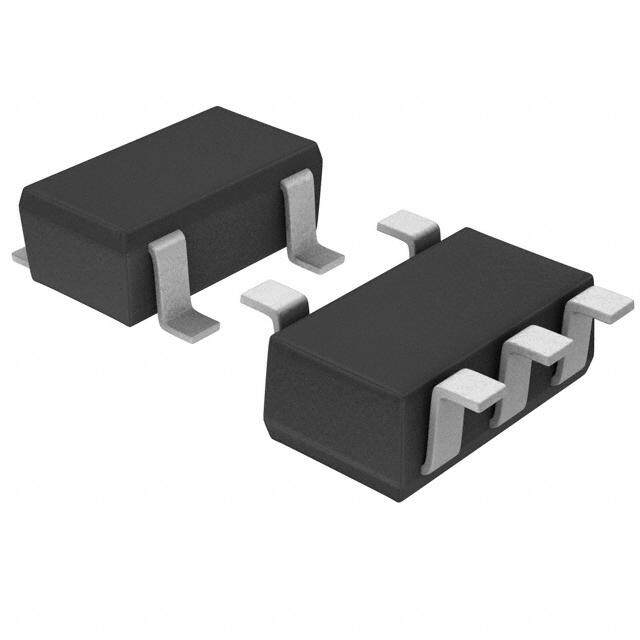
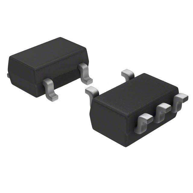
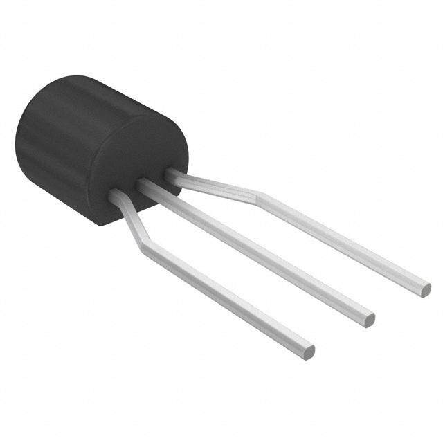
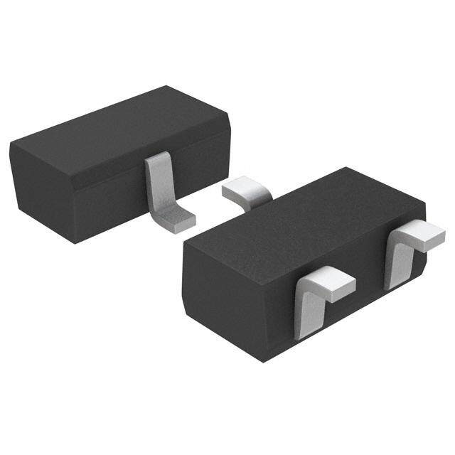
| 产品图片 |
|
| 产品型号 | MAX820TESE+ |
| rohs | 无铅 / 符合限制有害物质指令(RoHS)规范要求 |
| 产品系列 | - |
| 产品培训模块 | http://www.digikey.cn/PTM/IndividualPTM.page?site=cn&lang=zhs&ptm=25703http://www.digikey.cn/PTM/IndividualPTM.page?site=cn&lang=zhs&ptm=25705 |
| 供应商器件封装 | 16-SOIC |
| 包装 | 管件 |
| 受监控电压数 | 1 |
| 复位 | 高有效/低有效 |
| 复位超时 | 最小为 140 ms |
| 安装类型 | 表面贴装 |
| 封装/外壳 | 16-SOIC(0.154",3.90mm 宽) |
| 工作温度 | -40°C ~ 85°C |
| 标准包装 | 1 |
| 电压-阈值 | 3.06V |
| 类型 | 简单复位/加电复位 |
| 输出 | 推挽式,推挽式 |






- 商务部:美国ITC正式对集成电路等产品启动337调查
- 曝三星4nm工艺存在良率问题 高通将骁龙8 Gen1或转产台积电
- 太阳诱电将投资9.5亿元在常州建新厂生产MLCC 预计2023年完工
- 英特尔发布欧洲新工厂建设计划 深化IDM 2.0 战略
- 台积电先进制程称霸业界 有大客户加持明年业绩稳了
- 达到5530亿美元!SIA预计今年全球半导体销售额将创下新高
- 英特尔拟将自动驾驶子公司Mobileye上市 估值或超500亿美元
- 三星加码芯片和SET,合并消费电子和移动部门,撤换高东真等 CEO
- 三星电子宣布重大人事变动 还合并消费电子和移动部门
- 海关总署:前11个月进口集成电路产品价值2.52万亿元 增长14.8%



PDF Datasheet 数据手册内容提取
19-0147; Rev. 4; 11/05 Microprocessor and Nonvolatile Memory Supervisory Circuits General Description Features M The MAX792/MAX820 microprocessor (µP) supervisory ♦ Manual-Reset Input A circuits provide the most functions for power-supply ♦ 200ms Power-OK/Reset Time Delay X and watchdog monitoring in systems without battery ♦ Independent Watchdog Timer—Preset or Adjustable backup. Built-in features include the following: 7 • µP reset: Assertion of RESET and RESEToutputs during ♦ On-Board Gating of Chip-Enable Signals 9 power-up, power-down, and brownout conditions. ♦ Memory Write-Cycle Completion 2 RESETis guaranteed valid for VCCdown to 1V. ♦ 10ns (max) Chip-Enable Gate Propagation Delay / M • Manual-reset input. ♦ Voltage Monitor for Overvoltage Warning • Two-stage power-fail warning: A separate low-line ♦ ±2% Reset and Low-Line Threshold Accuracy A comparator compares VCC to a preset threshold (MAX820, external programming mode) X 120mV above the reset threshold; the low-line and Ordering Information 8 reset thresholds can be programmed externally. 2 • Watchdog fault output: Assertion of WDOif the watchdog PART** TEMP. RANGE PIN-PACKAGE 0 input is not toggled within a preset timeout MAX792_CPE 0°C to +70°C 16 Plastic DIP period. MAX792_CSE 0°C to +70°C 16 Narrow SO • Pulsed watchdog output: Advance warning of MAX792_C/D 0°C to +70°C Dice* impending WDOassertion from watchdog timeout that Ordering Information continued at end of data sheet. causes hardware shutdown. *Dice are tested at TA= +25°C, DC parameters only. • Write protection of CMOS RAM, EEPROM, or other **These parts offer a choice of five different reset threshold voltages. memory devices. Select the letter corresponding to the desired nominal reset threshold voltage and insert it into the blank to complete the part number. The MAX792 and MAX820 are identical, except the Devices in PDIP, SO and µMAX packages are available in both lead- MAX820 guarantees higher low-line and reset threshold ed and lead-free packaging. Specify lead free by adding the + sym- accuracy (±2%). bol at the end of the part number when ordering. Lead free not avail- able for CERDIP package. Applications SUFFIX RESET THRESHOLD (V) Computers L 4.62 M 4.37 Controllers T 3.06 Intelligent Instruments S 2.91 R 2.61 Critical µP Power Monitoring Typical Operating Circuit VCC 3 0.1µF VCC VCC 13 CE OUT 4 RESET IN/INT µP MAX792 RAM 5 LLIN/ CE IN 14 ADDRESS A0-A15 REFOUT DECODER 6 OVO 10 LOW LINE NMI 7 1 OVI RESET RESET 8 SWT MR 9 GND GND 12 ________________________________________________________________Maxim Integrated Products 1 For free samples and the latest literature, visit www.maxim-ic.com or phone 1-800-998-8800. For small orders, phone 1-800-835-8769.
Microprocessor and Nonvolatile Memory Supervisory Circuits 0 ABSOLUTE MAXIMUM RATINGS 2 Input Voltage (with respect to GND) Operating Temperature Ranges: 8 VCC.......................................................................-0.3V to +6V MAX792_C__/MAX820_C__...............................0°C to +70°C X All Other Inputs.......................................-0.3V to (VCC+ 0.3V) MAX792_E__/MAX820_E__.............................-40°C to +85°C Input Current MAX792_MJE__/MAX820_MJE__.................-55°C to +125°C A GND................................................................................25mA Storage Temperature Range.............................-65°C to +160°C All Other Outputs............................................................25mA Lead Temperature (soldering, 10s).................................+300°C M Continuous Power Dissipation (TA= +70°C) / Plastic DIP (derate 10.53mW/°C above +70°C)..........842mW 2 Narrow SO (derate 9.52mW/°C above +70°C)............762mW 9 CERDIP (derate 10.00mW/°C above +70°C)...............800mW 7 Stresses beyond those listed under “Absolute Maximum Ratings” may cause permanent damage to the device. These are stress ratings only, and functional X operation of the device at these or any other conditions beyond those indicated in the operational sections of the specifications is not implied. Exposure to A absolute maximum rating conditions for extended periods may affect device reliability. M ELECTRICAL CHARACTERISTICS (VCC= 2.75V to 5.5V, TA= TMINto TMAX, unless otherwise noted.) PARAMETER CONDITIONS MIN TYP MAX UNITS Operating Voltage Range 2.75 V (Note 1) Supply Current 70 150 µA RESET COMPARATOR MAX792L, MAX820L 4.50 4.62 4.75 MAX792M, MAX820M 4.25 4.37 4.50 MAX792R, MAX820R 2.55 2.61 2.70 MAX792S, MAX820S 2.85 2.91 3.00 Reset Threshold Voltage— MAX792T, MAX820T 3.00 3.06 3.15 Internal Threshold Mode V (VTH) MAX820L, TA= +25°C, VCCfalling 4.55 4.70 MAX820M, TA= +25°C, VCCfalling 4.30 4.45 MAX820R, TA= +25°C, VCCfalling 2.55 2.66 MAX820S, TA= +25°C, VCCfalling 2.85 2.96 MAX820T, TA= +25°C, VCCfalling 3.00 3.11 Reset Threshold Voltage MAX792, VCC= 5V or VCC= 3V 1.25 1.30 1.35 V External Threshold Mode (VTH) MAX820, VCC= 5V or VCC= 3V 1.274 1.30 1.326 RESET IN/INTMode Threshold Internal threshold mode 60 mV (Note 2) RESET IN/INTLeakage Current ±0.01 ±25 nA Reset Threshold Hysteresis 0.016 x VTH V Reset Comparator Delay VCCfalling 70 µs Reset Active Timeout Period VCCrising 140 200 280 ms ISINK= 50µA, VCC= 1V, VCCfalling 0.01 0.3 ISINK= 1.6mA 0.1 0.4 RESETOutput Voltage V ISOURCE= 1mA VCC- 1 ISOURCE= 100µA VCC- 0.5 ISINK= 1.6mA 0.1 0.4 RESET Output Voltage ISOURCE= 1mA VCC- 1 V ISOURCE= 100µA VCC- 0.5 2 _______________________________________________________________________________________
Microprocessor and Nonvolatile Memory Supervisory Circuits ELECTRICAL CHARACTERISTICS (continued) M (VCC= 2.75V to 5.5V, TA= TMINto TMAX, unless otherwise noted.) A PARAMETER CONDITIONS MIN TYP MAX UNITS X LOW-LINE COMPARATOR 7 Low-Line Threshold Voltage MAX792/MAX820L/M 50 120 210 9 mV (Internal Threshold Mode)—VTH MAX792/MAX820R/S/T 40 100 210 2 Low-Line Threshold Voltage MAX792, VCC= 5V OR VCC= 3V 1.25 1.30 1.35 / V M (External Programming Mode) MAX820, VCC= 5V OR VCC= 3V 1.274 1.30 1.326 Low-Line Hysteresis A 20 mV (Internal Threshold Mode) X LLIN/REFOUT Leakage Current 8 ±0.01 ±25 nA External Programming Mode 2 Low-Line Comparator Delay VCCfalling 450 µs 0 ISINK= 3.2mA 0.4 LOWLINEVoltage V ISOURCE= 1µA VCC- 1 LOWLINEShort-Circuit Current Output source current, VCC= 5.5V 10 50 µA WATCHDOG FUNCTION SWT connected to VCC, VCC = 5V 1.00 1.60 2.25 sec SWT connected to VCC, VCC = 3V 1.00 1.60 2.25 4.7nF capacitor connected from SWT to GND, Watchdog Timeout Period 70 VCC = 3V ms 4.7nF capacitor connected from SWT to GND, 100 VCC = 5V VCC= 5V 100 Watchdog Input Pulse Width VIL= 0V, VIH= VCC ns VCC= 3V 300 ISINK= 50µA, VCC= 1V, VCCfalling 0.01 0.30 ISINK= 1.6mA 0.1 0.4 WDOOutput Voltage V ISOURCE= 1mA VCC- 1 ISOURCE= 100µA VCC- 0.5 WDPOto WDODelay 70 ns WDPODuration 0.5 1.7 6.0 ms ISINK= 50µA, VCC= 1V, VCCfalling 0.01 0.3 ISINK= 1.6mA 0.1 0.4 WDPOOutput Voltage V ISOURCE= 1mA VCC- 1 ISOURCE= 100µA VCC- 0.5 VIH 0.75 x VCC VCC= 4.25V VIL 0.8 WDI Threshold Voltage V VIH 0.9 x VCC VCC= 2.55V VIL 0.2 WDI Input Current ±1 µA _______________________________________________________________________________________ 3
Microprocessor and Nonvolatile Memory Supervisory Circuits 0 ELECTRICAL CHARACTERISTICS (continued) 2 (VCC= +2.75V to +5.5V, TA= TMINto TMAX, unless otherwise noted.) 8 PARAMETER CONDITIONS MIN TYP MAX UNITS X OVERVOLTAGE COMPARATOR A OVI Input Threshold VCC= 5V or VCC= 3V 1.25 1.30 1.35 V M OVI Leakage Current ±0.01 ±25 nA ISINK= 3.2mA 0.4 / OVOOutput Voltage V 2 ISOURCE= 1µA VCC- 1 9 OVOShort-Circuit Current Output source current, VCC= 5.5V 10 50 µA 7 VOD= 100mV, OVI rising 13 X OVI to OVODelay µs VOD= 100mV, OVI falling 55 A CHIP-ENABLE GATING M VIH 0.75 x VCC VCC = 4.25V VIL 0.8 CEINThreshold Voltage V VIH 0.75 x VCC VCC= 2.55V VIL 0.2 CEIN Leakage Current Disabled mode ±0.005 ±1 µA CEIN to CEOUT Resistance Enabled mode VCC= 5V 75 150 Ω VCC= 3V 150 300 VCC= 5V 0.5 2.5 CEOUT Short-Circuit Current Disabled mode, CEOUT= 0V mA VCC= 3V 0.05 0.2 0.4 Chip-Enable Propagation Delay 50Ωsource impedance driver, VCC= 5V 6 10 ns (Note 3) CLOAD= 50pF VCC= 3V 8 13 Chip-Enable Output Voltage IOUT= -100µA VCC- 1 V High (Reset Active) IOUT= 10µA VCC- 0.5 Reset Active to CEOUT High VCC falling 15 µs MANUAL RESET MRMinimum Pulse Width 25 µs MRtoRESETPropagation Delay 12 µs MRThreshold Range 1.1 1.3 1.5 V VCC= 4.25V 5 23 80 MRPull-Up Current MR= 0V to VCC= 5.5V µA VCC= 2.5V 1 Note 1: The minimum operating voltage is 2.75V; however, the MAX792R and MAX820R are guaranteed to operate down to their preset reset thresholds. Note 2: Pulling RESET IN/INTbelow 60mV selects internal threshold mode and connects the internal voltage divider to the reset and low-line comparators. External programming mode allows an external resistor divider to set the low-line and reset thresholds (see Figure 4). Note 3: The Chip-Enable Propagation delay is measured from the 50% point at CEIN to the 50% point at CEOUT. 4 _______________________________________________________________________________________
Microprocessor and Nonvolatile Memory Supervisory Circuits __________________________________________Typical Operating Characteristics M (TA = +25°C, unless otherwise noted.) A X OVERVOLTAGE COMPARATOR RESET COMPARATOR 7 SUPPLY CURRENT vs. TEMPERATURE PROPAGATION DELAY vs. TEMPERATURE PROPAGATION DELAY vs. TEMPERATURE 9 19000 VCC = 5V SAWLLT O =U VTCPCUTS MAX792-1 70 MAX792-2 80 MAX792-3 2 µSUPPLY CURRENT (A) 8264135700000000 VCC = 4VVCC = 3V VCC = 2UVNLOADED µPROPAGATION DELAY (s) 546000 VVIIHN T=O 2 0VmOLV µPROPAGATION DELAY (s) 576000 V15CmC VF AOLVLEINRGDRIVE /MAX820 OVERDRIVE = 15mV EXTERNAL PROGRAMMING MODE 0 30 40 -60 -30 0 30 60 90 120 150 -60 -30 0 30 60 90 120 150 -60 -30 0 30 60 90 120 150 TEMPERATURE (°C) TEMPERATURE (°C) TEMPERATURE (°C) LOW-LINE COMPARATOR POWER-UP RESET DELAY NOMINAL WATCHDOG TIMEOUT PROPAGATION DELAY vs. TEMPERATURE vs. TEMPERATURE PERIOD vs. VCC 600 MAX792-3a 320500 MAX792-4 OD (s) 3.0 MAX792-5 500 RI µPROPAGATION DELAY (s) 430000 VVCCCC = = 3 5VV DELAY (ms) 121005000 L WATCHDOG TIMEOUT PE 212...055 200 VCC FALLING 50 MINA 15mV OVERDRIVE O EXTERNAL PROGRAMMING MODE N 100 0 1.0 -60 -30 0 30 60 90 120 150 -60 -30 0 30 60 90 120 150 2 3 4 5 TEMPERATURE (°C) TEMPERATURE (°C) VCC (V) _________________________________________________________________________________________________ 5
Microprocessor and Nonvolatile Memory Supervisory Circuits 0 Typical Operating Characteristics (continued) 2 (TA = +25°C, unless otherwise noted.) 8 X INTERNAL-MODE RESET THRESHOLD REF OUT VOLTAGE CHIP-ENABLE ON-RESISTANCE A vs. TEMPERATURE (NORMALIZED) vs. TEMPERATURE vs. TEMPERATURE M 11..110205 MAX792-6 11..3323 MAX792-7 128000 MAX792-8 2/ 1.075 1.31 160 VCC = 3V 9 LD 1.050 Ω) 140 VCE IN = 1.5V AX7 RESET THRESHO 110...009027055 REF OUT (V) 111...223890 N-RESISTANCE ( 11820000 O 60 M 0.950 THE RESET THRESHOLD IS SHOWN 1.27 40 VCC = 5V 0.925 NALOLR AMVAALIILZAEBDL TEO M 1A, XR7E9P2R/MESAEXN8T2I0NG 1.26 RESET IN / INT = 0V 20 VCE IN = 2.5V 0.900 1.25 0 -60 -30 0 30 60 90 120 150 -60 -30 0 30 60 90 120 150 -60 -30 0 30 60 90 120 150 TEMPERATURE (°C) TEMPERATURE (°C) TEMPERATURE (°C) WATCHDOG TIMEOUT PERIOD CHIP-ENABLE PROPAGATION DELAY vs. SWT LOAD CAPACITANCE vs. CE OUT LOAD CAPACITANCE OD (ms)11000kk MAX792-10 ns) 2105 VVDIMCCRPCEIV EI=NED R+=A 5 SN0VOVC UET RO=C 55E0VΩ MAX792-11 TCHDOG TIMEOUT PERI 1010k VCC = 5V VCC = 3V PROPAGATION DELAY ( 150 A W 10 0 1n 10n 100n 1m 0 25 50 75 100 125 150175 200 225250 CSWT (F) CLOAD (pF) 6 _______________________________________________________________________________________
Microprocessor and Nonvolatile Memory Supervisory Circuits ______________________________________________________________Pin Description M A PIN NAME FUNCTION X Active-Low Reset Output goes low whenever VCCfalls below the reset threshold in internal thresh- 7 1 RESET old programming mode, or RESET IN falls below 1.30V in external threshold programming mode. 9 RESETremains low for 200ms typ after the threshold is exceeded on power-up. 2 / 2 RESET Reset is the inverse of RESET. M 3 VCC Input Supply Voltage A X Reset-Input/Internal-Mode Select. Connect this input to GND to select internal threshold mode. 4 RESET IN/INT Select external programming mode by pulling this input 600mV or higher through an external volt- 8 age divider. 2 0 Low-Line Input/Reference Output connects directly to the low-line comparator in external program- 5 LLIN/REF OUT ming mode (RESET IN/INT≥600mV). Connects directly to the internal 1.30V reference in internal threshold mode (RESET IN/INT≤ 60mV). Overvoltage Comparator Output goes low when OVI is greater than 1.30V. This is an uncommitted 6 OVO comparator and has no effect on any other internal circuitry. Inverting Input to the Overvoltage Comparator. When OVI is greater than 1.30V, OVOgoes low. 7 OVI Connect OVI to GND or VCCwhen not used. Set Watchdog-Timeout Input. Connect this input to VCCto select the default 1.6sec watchdog timeout period. Connect a capacitor between this input and GND to select another watchdog- 8 SWT timeout period. Watchdog timeout period = k x (capacitor value in nF)mV, where k = 27 for VCC= 5V and k = 16.2 for VCC= 3V. If the watchdog function is unused, connect SWT to VCC. Manual-Reset Input. This input can be tied to an external momentary pushbutton switch, or to a 9 MR logic gate output. Internally pulled up to VCC. Low-Line Output. LOW LINEgoes low 120mV above the reset threshold in internal threshold mode, 10 LOW LINE or when LLIN/REFOUT goes below 1.30V in external programming mode. Watchdog Input. If WDI remains either high or low for longer than the watchdog timeout period, 11 WDI WDPOpulses low and WDOgoes low. WDOremains low until the next transition at WDI. Connect to GND or VCCif unused. 12 GND Ground Chip-Enable Output. CEOUT goes low only when CEIN is low and reset is not asserted. If CEIN is 13 CEOUT low when reset is asserted, CEOUT will stay low for 15µs or until CEIN goes high, whichever occurs first. Chip-Enable Input—the input to the chip-enable transmission gate. Connect to GND or VCCif not 14 CEIN used. Watchdog Output. WDOgoes low if WDI remains either high or low longer than the watchdog time- 15 WDO out period. WDOreturns high on the next transition at WDI. Watchdog-Pulse Output. Upon the absence of a transition at WDI, WDPOwill pulse low for a mini- 16 WDPO mumof 500µs. WDPOprecedes WDOby typically 70ns. _______________________________________________________________________________________ 7
Microprocessor and Nonvolatile Memory Supervisory Circuits 0 Detailed Description External Programming Mode 2 Connecting RESET IN/INT to a voltage above 600mV Manual-Reset Input 8 selects external programming mode. In this mode, the X Many µP-based products require manual-reset capabil- low-line and reset comparators disconnect from the inter- ity, allowing the operator to initiate a reset. The manu- nal voltage divider and connect to LLIN/REFOUT and A al/external-reset input (MR) can connect directly to a RESET IN/INT, respectively (Figure 1). This mode allows M switch without an external pull-up resistor or debounc- flexibility in determining where in the operating voltage ing network. MR internally connects to a 1.30V com- range the NMI and reset are generated. Set the low-line / 2 parator, and has a high-impedance pull-up to VCC, as and reset thresholds with an external resistor divider, as in 9 shown in Figure 1. The propagation delay from assert- Figure 4b or Figure 4c. RESET typically remains valid for ing MR to reset asserted is typically 12µs. Pulsing MR V down to 2.5V; RESET is guaranteed to be valid with 7 CC low for a minimum of 25µs asserts the reset function V down to 1V. X CC (see Reset Function section). The reset output remains Calculate the values for the resistor voltage divider in A active as long as MR is held low, and the reset timeout Figure 4b using the following equations: period begins after MR returns high (Figure 2). To pro- M vide extra noise immunity in high-noise environments, 1) R3 = (1.30 x VCCMAX)/(VLOW LINEx IMAX) pull MRup to VCCwith a 100kΩresistor. 2) R2 = [(1.30 x VCCMAX)/(VRESETx IMAX)] - R3 Use MRas either a digital logic input or as a second low- 3) R1 = (V MAX/I ) - (R2 + R3). CC MAX line comparator. Normal TTL/CMOS levels can be First choose the desired maximum current through the wire-OR connected via pull-down diodes (Figure 3), voltage divider (I ) when V is at its highest (V and open-drain/collector outputs can be wire-ORed MAX CC CC MAX). There are two things to consider here. First, I directly. MAX contributes to the overall supply current for the circuit, so Monitoring the Regulated Supply you would generally make it as small as possible. Second, I cannot be too small or leakage currents will MAX The MAX792/MAX820 offer two modes for monitoring adversely affect the programmed threshold voltages; 5µA the regulated supply and providing reset and non- is often appropriate. Determine R3 after you have chosen maskable interrupt (NMI) signals to the µP: internal I . Use the value for R3 to determine R2, then use both MAX threshold mode uses the factory preset low-line and R2 and R3 to determine R1. reset thresholds, and external programming mode For example, to program a 4.75V low-line threshold and a allows the low-line and reset thresholds to be pro- 4.4V reset threshold, first choose I to be 5µA when grammed externally using a resistor voltage divider MAX V = 5.5V and substitute into equation 1. (Figure 4). CC R3 = (1.30 x 5.5)/(4.75 x 5E-6) = 301.05kΩ. Internal Threshold Mode 301kΩ is the nearest standard 0.1% value. Substitute Connecting the reset-input/internal-mode select pin into equation 2: (RESET IN/INT) to ground selects internal threshold R2 = [(1.30 x 5.5)/(4.4 x 5E-6)] - 301kΩ= 23.95kΩ. mode (Figure 4a). In this mode, the low-line and reset thresholds are factory preset by an internal voltage The nearest 0.1% resistor value is 23.7kΩ. Finally, sub- divider (Figure 1) to the threshold voltages specified in stitute into equation 3: the Electrical Characteristics (Reset Threshold Voltage R1 = (5.5/5E-6) - (23.7kΩ+ 301kΩ) = 775kΩ. and Low-Line Threshold Voltage). Connect the low-line The nearest 0.1% value resistor is 787kΩ. Determine the output (LOWLINE) to the µP NMI pin, and connect the actual low-line threshold by rearranging equation 1 and active-high reset output (RESET) or active-low reset plugging in the standard resistor values. The actual low- output (RESET) to the µP reset input pin. line threshold is 4.75V and the actual reset threshold is Additionally, the low-line input/reference-output pin 4.40V. An additional resistor allows the MAX792/MAX820 (LLIN/REFOUT) connects to the internal 1.30V refer- to monitor the unregulated supply and provide an NMI ence in internal threshold mode. Buffer LLIN/REFOUT before the regulated supply begins to fall (Figure 4c). with a high-impedance buffer to use it with external Both of these thresholds will vary from circuit to circuit circuitry. In this mode, when V is falling, LOWLINE is CC with resistor tolerance, reference variation, and compara- guaranteed to be asserted prior to reset assertion. tor offset variation. The initial thresholds for each circuit will also vary with temperature due to reference and off- set drift. For highest accuracy, use the MAX820. 8 _______________________________________________________________________________________
Microprocessor and Nonvolatile Memory Supervisory Circuits M VCC 3 A X 7 2 VCC RESET 9 * RESET 2 RESET IN/ 4 COMPARATOR INT RESET /M GENERATOR 1 RESET A VCC X LLIN/ 5 10 REFOUT LOW LINE 8 VCC LOW-LINE VCC COMPARATOR 2 CHIP-ENABLE 0 9 VCC OUTPUT P MR CONTROL MANUAL RESET COMPARATOR 1.30V VCC INTERNAL/ EXTERNAL MODE CONTROL 60mV INTERNAL P EXTERNAL 14 13 CE IN CE OUT TIMEBASE FOR N RESET AND WATCHDOG 16 8 WATCHDOG WDPO SWT 15 TIMER WDO 11 WDI WATCHDOG VCC TRANSITION MAX792 DETECTOR OVERVOLTAGE MAX820 COMPARATOR 6 OVO 7 OVI 12 * SWITCHES ARE SHOWN IN INTERNAL GND THRESHOLD MODE POSITION Figure 1. MAX792/MAX820 Block Diagram _______________________________________________________________________________________ 9
Microprocessor and Nonvolatile Memory Supervisory Circuits 0 2 VIN 25µs MIN 8 MR 3 X 12µs TYP VCC RESET A 4 RESET IN/INT RESET 2 TO µP M CE IN OV MAX792 2/ CE OUT 15µs TYP 5 LLIN/REFOUT RESET 1 TO µP 9 7 LOW LINE 10 TO µP NMI X Figure 2. Manual-Reset Timing Diagram A GND M MANUAL RESET 12 9 MR Figure 4a. Connection for Internal Threshold Mode * OTHER RESET MAX792 VIN * SOURCES . MAX820 . . 3 R1 VCC RESET IN/INT RESET 2 TO µP * DIODES NOT REQUIRED ON OPEN-DRAIN OUTPUTS Figure 3. Diode "OR" connections allow multiple reset sources R2 MAX792 to connect to MR. LLIN/REFOUT RESET 1 TO µP Low-Line Output In internal threshold mode, the low-line comparator R3 LOW LINE 10 TO µP NMI monitors V with a threshold voltage typically 120mV CC above the reset threshold, and with 15mV of hysteresis. GND For normal operation (V above the reset threshold), 12 CC LOWLINEis pulled to VCC. Use LOWLINEto provide an NMI R3 = 1.30V x VCC MAX to the µP, as described in the previous section, when VLOW LINE x IMAX V begins to fall (Figure 4). CC R2 = 1.30V x VCC MAX – R3 IMAX = THE MAXIMUM DESIRED CURRENT VRESET x IMAX THROUGH THE VOLTAGE DIVIDED. Reset Function R1 = VCC MAX – (R2 + R3) The MAX792/MAX820 provide both RESET and RESET IMAX outputs. The RESET and RESET outputs ensure that the µP powers up in a known state, and prevent code-exe- Figure 4b. Connection for External Threshold Programming Mode cution errors during power-up, power-down, or brownout conditions. When reset is asserted, all the internal counters are The reset function will be asserted during the following reset, the watchdog output (WDO) and watchdog-pulse conditions: output (WDPO) are set high, and the set watchdog-time- out input (SWT) is set to (V - 0.6V) if it is not already CC 1) V less than the programmed reset threshold. CC connected to V (for internal timeouts). The chip- CC 2) MRless than 1.30V typ. enable transmission gate is also disabled while reset is 3) Reset remains asserted for 200ms typ after V asserted; the chip-enable input (CE IN) becomes high CC rises above the reset threshold or after MR has impedance and the chip-enable output (CE OUT) is exceeded 1.30V typ. pulled up to VCC. 10 ______________________________________________________________________________________
Microprocessor and Nonvolatile Memory Supervisory Circuits M A REGULATOR RESET 1 TO µP RESET X MAX792 10k 7 R3 VCC MAX820 9 RESET IN/INT RESET 2 TO µP 2 R1 / R4 MAX792 M MAX820 A LLIN/REFOUT RESET 1 TO µP X Figure 5. Adding an external pull-down resistor ensures RESET R2 is valid with VCCdown to GND. 8 LOW LINE 10 TO µP NMI 2 0 GND VOLTAGE REGULATOR VLOW LINE = 1.3 ( R1 + R2) R2 VRESET = 1.3 ( R 3 + R4) R4 3 VCC Figure 4c. Alternative Connection for External Programming Mode MAX792 Reset Outputs (RESET and RESET) MAX820 The RESEToutput is active low and typically sinks 1.6mA 7 OVI at 0.1V. When deasserted, RESETsources 1.6mA at typi- OVO 6 OVERVOLTAGE cally V - 1.5V. The RESET output is the inverse of CC RESET.RESETis guaranteed to be valid down to V = 1V, CC and an external 10kΩ pull-down resistor on RESET 1.30V ensures that it will be valid with V down to GND CC (Figure 5). As V goes below 1V, the gate drive to the CC GND RESEToutput switch reduces accordingly, increasing the 12 r and the saturation voltage. The 10kΩ pull-down DS(ON) resistor ensures that the parallel combination of switch plus resistor will be around 10kΩ and the saturation voltage will be below 0.4V while sinking 40µA. When Figure 6. Detecting an Overvoltage Condition using an external pull-down resistor of 10kΩ, the high state for the RESET output with V = 4.75V is typically CC Watchdog Function 4.60V. The watchdog monitors µP activity via the watchdog Overvoltage Comparator input (WDI). If the µP becomes inactive,WDOand WDPO The overvoltage comparator is an uncommitted com- are asserted. To use the watchdog function, connect parator that has no effect on the operation of other chip WDI to a µP bus line or I/O line. If WDI remains high or functions. Use this input to provide overvoltage indica- low for longer than the watchdog timeout period (1.6s tion by connecting a voltage divider from the input sup- nominal), WDPOand WDOare asserted, indicating a soft- ply, as in Figure 6. ware fault condition (see Watchdog-Pulse Output and Watchdog Outputsections). Connect OVI to ground if the overvoltage function is not used. OVO goes low when OVI goes above 1.30V. With Watchdog Input OVI below 1.30V, OVO is actively pulled to V and can CC source1µA. If the watchdog function is unused, connect WDI to VCC or GND. A change of state (high-to-low, low-to-high, or a minimum 100ns pulse) at WDI during the watchdog period resets the watchdog timer. The watchdog timer ______________________________________________________________________________________ 11
Microprocessor and Nonvolatile Memory Supervisory Circuits 0 2 MIN 100ns (VCC = 5V) MIN 300ns (VCC = 3V) 8 1.6s VCC X A WDI VCC3 0.1µF VCC WDPO M MAX792 µP POWER MAX820 / 70ns 1 2 WDO RESET RESET 11 9 WDI I/O 16 7 WDPO X VCC = 5V 9 15 CLOCK VCCQ MR WDO D A Figure 7. WDI, WDO,and WDPOTiming Diagram GND CLEAR Q M +5V 12 * CONSTEWCOUTIVE default is 1.6s. Select alternative timeout periods by WATCHDOG connecting an external capacitor from SWT to GND FAULT 0.1µF INDICATION (see Selecting an Alternative Watchdog Timeout sec- tion). When VCCis below the reset threshold, the watch- REACTIVATE dog function is disabled. * FOR SYSTEM RESET ON EVERY 4.7k WATCHDOG FAULT, OMIT THE Watchdog Output FLIP-FLOP, AND DIODE–OR CONNECT WDO TO MR. WDOremains high if there is a transition or pulse at WDI during the watchdog timeout period. The watchdog function is disabled and WDO is a logic high when V CC is below the reset threshold. If a system reset is desired Figure 8. Two consecutive watchdog faults latch the system in on every watchdog fault, simply diode-OR connect WDO reset. to MR (Figure 8). When a watchdog fault occurs in this mode, WDO goes low, pulling MR low and causing a reset pulse to be issued. As soon as reset is asserted, WDI, WDO remains low and the next WDPO following a the watchdog timer clears and WDO goes high. With second watchdog timeout period clocks a logic low to WDOconnected to MR, a continuous high or low on WDI the Q output, pulling MR low and causing the will cause 200ms reset pulses to be issued every MAX792/MAX820 latch in reset. If the watchdog timer is 1.6sec (SWT connected to V ). When reset is not reset by a transition at WDI, WDO will go high and the CC asserted, if no transition occurs at WDI during the flip-flop’s Q output will remain high. Thus a system watchdog timeout period, WDO goes low 70ns after the shutdown is only caused by two successive watchdog falling edge of WDPOand remains low until the next tran- faults. sition at WDI (Figure 7). A single additional flip-flop can Selecting an Alternative Watchdog Timeout Period force the system into a hardware shutdown if there are two successive watchdog faults (Figure 8). When the The SWT input controls the watchdog timeout period. MAX792/MAX820 are operated from a 5V supply, WDO Connecting SWT to VCC selects the internal 1.6sec has a 2 x TTL output characteristic. watchdog timeout period. Select an alternative watch- dog timeout period by connecting a capacitor between Watchdog-Pulse Output SWT and GND. Do not leave SWT floating and do not connect it to ground. The following formula determines As described in the preceding section, WDPO can be the watchdog timeout period: used as the clock input to an external D flip-flop. Upon the absence of a watchdog edge or pulse at WDI at the Watchdog Timeout Period = end of a watchdog timeout period, WDPO will pulse low k x (capacitor value in nF)ms for 1.7ms. The falling edge of WDPO precedes WDO by where k = 27 for V = 3V, and k = 16.2 for V = 5V. CC CC 70ns. Since WDO is high when WDPOgoes low, the flip- This applies for capacitor values in excess of 4.7nF. If flop’s Q output remains high after WDOgoes low (Figure the watchdog function is unused, connect SWT to V . 8). If the watchdog timer is not reset by a transition at CC 12 ______________________________________________________________________________________
Microprocessor and Nonvolatile Memory Supervisory Circuits Chip-Enable Signal Gating M The MAX792/MAX820 provide internal gating of chip- VCC A enable (CE) signals, which prevents erroneous data RESET THRESHOLD X from corrupting CMOS RAM in the event of an under- voltage condition. The MAX792/MAX820 use a series CE IN 7 transmission gate from CEIN to CEOUT (Figure 1). 9 During normal operation (reset not asserted), the CE 2 transmission gate is enabled and passes all CE transi- CE OUT 15µs / M tions. When reset is asserted, this path becomes dis- 70µs 70µs abled, preventing erroneous data from corrupting the A RESET CMOS RAM. The 10ns max CE propagation delay from CE IN to CE OUT enables the MAX792/MAX820 to be X RESET used with most µPs. If CE IN is low when reset asserts, 8 CE OUT remains low for a short period to permit com- 2 pletion of the current write cycle. 0 Figure 9. Reset and Chip-Enable Timing Chip-Enable Input The CE transmission gate is disabled and CE IN is high impedance (disabled mode) while reset is asserted. +5V 3 During a power-down sequence when V passes the CC VCC reset threshold, the CE transmission gate disables and CE IN immediately becomes high impedance if the volt- MAX792 age at CEIN is high. If CEIN is low when reset is assert- MAX820 ed, the CE transmission gate will disable at the moment 14 13 CE IN CE OUT CE IN goes high or 15µs after reset is asserted, whichever occurs first (Figure 9). This permits the cur- 50Ω DRIVER CLOAD rent write cycle to complete during power-down. GND During a power-up sequence, the CE transmission gate 12 remains disabled and CE IN remains high impedance regardless of CEIN activity, until reset is deasserted fol- lowing the reset timeout period. While disabled, CE IN is high impedance. When the CE Figure 10. CE Propagation Delay Test Circuit transmission gate is enabled, the impedance of CE IN will appear as a 75Ω (V = 5V) resistor in series with Chip-Enable Output CC the load at CEOUT. When the CE transmission gate is enabled, the imped- ance of CE OUT is equivalent to 75Ω in series with the The propagation delay through the CE transmission source driving CE IN. In the disabled mode, the 75Ω gate depends on V the source impedance of the CC, transmission gate is off and an active pull-up connects drive connected to CE IN, and the loading on CE OUT from CE OUT to V . This source turns off when the (see the Chip-Enable Propagation Delay vs. CE OUT CC transmission gate is enabled. Load Capacitance graph in the Typical Operating Characteristics). The CE propagation delay is produc- Applications Information tion tested from the 50% point on CE IN to the 50% point on CE OUT using a 50Ω driver and 50pF of load Connect a 0.1µF ceramic capacitor from VCC to GND, as close to the device pins as possible. This reduces capacitance (Figure 10). For minimum propagation the probability of resets due to high-frequency power- delay, minimize the capacitive load at CEOUT, and use supply transients. In a high-noise environment, addi- a low-output-impedance driver. tional bypass capacitance from V to ground may be CC required. If long leads connect to the chip inputs, ensure that these lines are free from ringing, etc., which would forward bias the chip’s protection diodes. ______________________________________________________________________________________ 13
Microprocessor and Nonvolatile Memory Supervisory Circuits 0 2 +5V RP* 8 CE 3 RAM 1 BUFFER X VCC CE TO OTHER A VCC SYSTEM RESET MAX792 CE 3 INPUTS M MAX820 14 13 RAM 2 VCC VCC 2/ CE IN CE OUT CE RESET 1 4.7k RESET µP 9 CE RAM 3 7 GND MAX792 CE X 12 MAX820 A CE M *MTHAEX NIMUUMMB ERRP OVFA LRUAEM DSE.PENDS ON CE RAM 4 GND12 GND MINIMUM RP VALUE IS 1kΩ ACTIVE-HIGH CE LINES FROM LOGIC Figure 11. Alternate CE Gating Figure 12. Interfacing to µPs with Bidirectional RESETPins Alternative Chip-Enable Gating going VCC pulses, starting at 5V and ending below the reset threshold by the magnitude indicated (reset- Using memory devices with both CE and CE inputs comparator overdrive). The graph shows the maximum allows the MAX792/MAX820 CE propagation delay pulse width a negative-going VCC transient may typi- to be bypassed. To do this, connect CE IN to ground, cally have without causing a reset pulse to be issued. pull up CE OUT to VCC, and connect CE OUT to the CE As the amplitude of the transient increases (i.e., goes input of each memory device (Figure 11). The CE input farther below the reset threshold), the maximum allow- of each memory device then connects directly to the able pulse width decreases. Typically, a VCC transient chip-select logic, which does not have to be gated by that goes 100mV below the reset threshold and lasts for the MAX792/MAX820. 30µs or less will not cause a reset pulse to be issued. Interfacing to µPs with Bidirectional A 100nF bypass capacitor mounted close to the VCC Reset Inputs pin provides additional transient immunity. µPs with bidirectional reset pins, such as the Motorola 68HC11 series, can contend with the MAX792/MAX820 RESEToutput. If, for example, the MAX792/MAX820 RESET 100 oicnuodtnpenuteetc rimts a ian 4sa.st7eekr Ωtleodgre ihcsii gsltehov rae bnlsed t mwtheaeey nµ r Pteh sweu aMltn.A tsTX ot7o 9 a2pv/uoMlild Ait X tl8ho2iws0,, ON (µs) 80 VCC = 5V MAX791 -13 RESET output and the µP reset I/O, as in Figure 12. RATI TA = +25°C U Buffer the MAX792/MAX820 RESET output to other sys- D 60 T tem components. N E SI N Negative-Going VCC Transients RA 40 T While issuing resets to the µP during power-up, power- M U M down, and brownout conditions, these supervisors are XI 20 relatively immune to short-duration negative-going VCC MA transients (glitches). It is usually undesirable to reset 0 the µP when VCCexperiences only small glitches. 10 100 1000 10,000 Figure 13 shows maximum transient duration vs. reset- RESET COMPARATOR OVERDRIVE, (VTH - VCC) (mV) comparator overdrive, for which reset pulses are not generated. The graph was produced using negative- Figure 13.Maximum Transient Duration Without Causing a Reset Pulse vs. Reset-Comparator Overdrive 14 ______________________________________________________________________________________
Microprocessor and Nonvolatile Memory Supervisory Circuits _Ordering Information (continued) Pin Configuration M A PART** TEMP. RANGE PIN-PACKAGE TOP VIEW X MAX792_EPE -40°C to +85°C 16 Plastic DIP MAX792_ESE -40°C to +85°C 16 Narrow SO RESET 1 16 WDPO 7 MAX792_EJE -40°C to +85°C 16 CERDIP RESET 2 15 WDO 9 MAX792_MJE -55°C to +125°C 16 CERDIP VCC 3 MAX792 14 CE IN 2 MAX820_CPE -0°C to +70°C 16 Plastic DIP RESET IN/INT 4 MAX820 13 CE OUT /M MAX820_CSE -0°C to +70°C 16 Narrow SO LLIN/REFOUT 5 12 GND A MAX820_EPE -40°C to +85°C 16 Plastic DIP MAX820_ESE -40°C to +85°C 16 Narrow SO OVO 6 11 WDI X MAX820_EJE -40°C to +85°C 16 CERDIP OVI 7 10 LOW LINE 8 MAX820_MJE -55°C to +125°C 16 CERDIP SWT 8 9 MR 2 *Dice are tested at TA= +25°C, DC parameters only. 0 **These parts offer a choice of five different reset threshold volt- DIP/SO ages. Select the letter corresponding to the desired nominal reset threshold voltage and insert it into the blank to complete the part number. ___________________Chip Topography Devices in PDIP, SO and µMAX packages are available in both leaded and lead-free packaging. Specify lead free by adding the + symbol at the end of the part number when ordering. Lead RESET WDO free not available for CERDIP package. RESET WDPO CE IN SUFFIX RESET THRESHOLD (V) CE OUT L 4.62 VCC M 4.37 T 3.06 S 2.91 RESET IN/ R 2.61 INT 0.078" GND LLIN/ (1.981mm) REF OUT OVO WDI OVI SWTMR LOWLINE 0.070" (1.778mm) TRANSISTOR COUNT: 950 SUBSTRATE CONNECTED TO VCC ______________________________________________________________________________________ 15
Microprocessor and Nonvolatile Memory Supervisory Circuits 0 ________________________________________________________Package Information 2 X8 N DIM MIINNCHEMSAX MMIILNLIMETMERASX SOICW.EPS A 0.093 0.104 2.35 2.65 A A1 0.004 0.012 0.10 0.30 B 0.014 0.019 0.35 0.49 M C 0.009 0.013 0.23 0.32 E H e 0.050 1.27 E 0.291 0.299 7.40 7.60 / H 0.394 0.419 10.00 10.65 2 L 0.016 0.050 0.40 1.27 9 VARIATIONS: 7 1 INCHES MILLIMETERS X TOP VIEW DIM MIN MAX MIN MAX N MS013 D 0.398 0.413 10.10 10.50 16 AA A D 0.447 0.463 11.35 11.75 18 AB D 0.496 0.512 12.60 13.00 20 AC D 0.598 0.614 15.20 15.60 24 AD M D D 0.697 0.713 17.70 18.10 28 AE A C e B A1 0∞-8∞ L FRONT VIEW SIDE VIEW PROPRIETARY INFORMATION TITLE: PACKAGE OUTLINE, .300" SOIC APPROVAL DOCUMENT CONTROL NO. REV. 1 21-0042 B 1 INCHES MILLIMETERS CN .EPS DIM MIN MAX MIN MAX SOI A 0.053 0.069 1.35 1.75 N A1 0.004 0.010 0.10 0.25 B 0.014 0.019 0.35 0.49 C 0.007 0.010 0.19 0.25 e 0.050 BSC 1.27 BSC E 0.150 0.157 3.80 4.00 E H H 0.228 0.244 5.80 6.20 L 0.016 0.050 0.40 1.27 VARIATIONS: 1 INCHES MILLIMETERS TOP VIEW DIM MIN MAX MIN MAX N MS012 D 0.189 0.197 4.80 5.00 8 AA D 0.337 0.344 8.55 8.75 14 AB D 0.386 0.394 9.80 10.00 16 AC D A C e B A1 0∞-8∞ L FRONT VIEW SIDE VIEW PROPRIETARY INFORMATION TITLE: PACKAGE OUTLINE, .150" SOIC APPROVAL DOCUMENT CONTROL NO. REV. 1 21-0041 B 1 Maxim cannot assume responsibility for use of any circuitry other than circuitry entirely embodied in a Maxim product. No circuit patent licenses are implied. Maxim reserves the right to change the circuitry and specifications without notice at any time. 16 ____________________Maxim Integrated Products, 120 San Gabriel Drive, Sunnyvale, CA 94086 408-737-7600 © 2005 Maxim Integrated Products Printed USA is a registered trademark of Maxim Integrated Products, Inc.

 Datasheet下载