ICGOO在线商城 > 集成电路(IC) > PMIC - 监控器 > STM809LWX6F
 Datasheet下载
- 型号: STM809LWX6F
- 制造商: STMicroelectronics
- 库位|库存: xxxx|xxxx
- 要求:
| 数量阶梯 | 香港交货 | 国内含税 |
| +xxxx | $xxxx | ¥xxxx |
查看当月历史价格
查看今年历史价格
STM809LWX6F产品简介:
ICGOO电子元器件商城为您提供STM809LWX6F由STMicroelectronics设计生产,在icgoo商城现货销售,并且可以通过原厂、代理商等渠道进行代购。 STM809LWX6F价格参考。STMicroelectronicsSTM809LWX6F封装/规格:PMIC - 监控器, 推挽式,图腾柱 监控器 1 通道 SOT-23-3。您可以下载STM809LWX6F参考资料、Datasheet数据手册功能说明书,资料中有STM809LWX6F 详细功能的应用电路图电压和使用方法及教程。
STM809LWX6F 是 STMicroelectronics(意法半导体)的一款 PMIC(电源管理集成电路),属于 PMIC - 监控器类别。该型号主要应用于需要高效电源管理和系统监控的场景,以下是其典型应用场景:

1. 嵌入式系统
   STM809LWX6F 可用于各种嵌入式系统中,提供精确的电压监测和保护功能。例如,在工业控制设备、家用电器或物联网终端中,它能够确保系统在安全电压范围内运行,避免因过压或欠压导致的损坏。

2. 消费电子设备
   在消费电子产品(如智能手表、健康监测设备、便携式音频设备等)中,这款 PMIC 能够优化电池使用效率,同时实时监控电池状态,延长设备续航时间。

3. 通信设备
   对于网络路由器、调制解调器或其他通信设备,STM809LWX6F 提供可靠的电源管理和复位功能,确保设备在复杂环境下稳定运行。

4. 汽车电子
   在汽车电子系统中(如信息娱乐系统、车载诊断设备等),该芯片可以监测电源电压并触发必要的保护机制,防止因电源波动导致的系统故障。

5. 工业自动化
   在工业自动化领域,这款 PMIC 适用于 PLC(可编程逻辑控制器)、传感器模块和其他关键设备中,提供高精度的电压监控和复位功能,保障系统的可靠性和安全性。

6. 医疗设备
   在便携式医疗设备(如血糖仪、脉搏血氧仪等)中,STM809LWX6F 的低功耗特性和高精度监控能力使其成为理想选择,确保设备的持续稳定运行。

总之,STM809LWX6F 适合需要高效电源管理、电压监控和系统保护的各种应用场合,尤其在对可靠性要求较高的环境中表现突出。
| 参数 | 数值 |
| 产品目录 | 集成电路 (IC)半导体 |
| 描述 | IC MPU RESET CIRC 4.63V SOT23监控电路 4.63V Reset 140ms |
| 产品分类 | |
| 品牌 | STMicroelectronics |
| 产品手册 | |
| 产品图片 |
|
| rohs | 符合RoHS无铅 / 符合限制有害物质指令(RoHS)规范要求 |
| 产品系列 | 电源管理 IC,监控电路,STMicroelectronics STM809LWX6F- |
| NumberofInputsMonitored | 1 Input |
| 数据手册 | |
| 产品型号 | STM809LWX6F |
| 产品培训模块 | http://www.digikey.cn/PTM/IndividualPTM.page?site=cn&lang=zhs&ptm=30015 |
| 产品目录页面 | |
| 产品种类 | 监控电路 |
| 人工复位 | No Manual Reset |
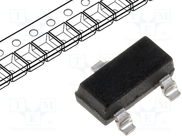
| 供应商器件封装 | SOT-23-3 |
| 其它名称 | 497-3378-1 |
| 其它有关文件 | http://www.st.com/web/catalog/sense_power/FM1946/SC665/PF78091?referrer=70071840 |
| 功率失效检测 | No |
| 包装 | 剪切带 (CT) |
| 受监控电压数 | 1 |
| 商标 | STMicroelectronics |
| 复位 | 低有效 |
| 复位超时 | 最小为 140 ms |
| 安装类型 | 表面贴装 |
| 安装风格 | SMD/SMT |
| 封装 | Reel |
| 封装/外壳 | TO-236-3,SC-59,SOT-23-3 |
| 封装/箱体 | SOT-23-3 |
| 工作温度 | -40°C ~ 85°C |
| 工作电源电流 | 15 uA |
| 工厂包装数量 | 3000 |
| 最大功率耗散 | 320 mW |
| 最大工作温度 | + 85 C |
| 最小工作温度 | - 40 C |
| 标准包装 | 1 |
| 欠电压阈值 | 4.56 V |
| 电压-阈值 | 4.63V |
| 电池备用开关 | No Backup |
| 电源电压-最大 | 5.5 V |
| 电源电压-最小 | 1 V |
| 监视器 | No Watchdog |
| 类型 | Voltage Supervisory |
| 系列 | STM809 |
| 芯片启用信号 | No Chip Enable |
| 被监测输入数 | 1 Input |
| 输出 | 推挽式,图腾柱 |
| 输出类型 | Active Low, Push-Pull |
| 过电压阈值 | 4.7 V |
| 重置延迟时间 | 280 ms |
| 阈值电压 | 3 V, 3.3 V, 5 V |


- 商务部:美国ITC正式对集成电路等产品启动337调查
- 曝三星4nm工艺存在良率问题 高通将骁龙8 Gen1或转产台积电
- 太阳诱电将投资9.5亿元在常州建新厂生产MLCC 预计2023年完工
- 英特尔发布欧洲新工厂建设计划 深化IDM 2.0 战略
- 台积电先进制程称霸业界 有大客户加持明年业绩稳了
- 达到5530亿美元!SIA预计今年全球半导体销售额将创下新高
- 英特尔拟将自动驾驶子公司Mobileye上市 估值或超500亿美元
- 三星加码芯片和SET,合并消费电子和移动部门,撤换高东真等 CEO
- 三星电子宣布重大人事变动 还合并消费电子和移动部门
- 海关总署:前11个月进口集成电路产品价值2.52万亿元 增长14.8%


PDF Datasheet 数据手册内容提取
STM809, STM810 STM811, STM812 Reset circuit Features ■ Precision monitoring of 3 V, 3.3 V, and 5 V supply voltages ■ Two output configurations – Push-pull RST output (STM809/811) – Push-pull RST output (STM810/812) SOT23-3 (WX) ■ 140 ms reset pulse width (min) ■ Low supply current - 6 µA (typ) ■ Guaranteed RST/RST assertion down to V = 1.0 V CC ■ Operating temperature: –40 °C to 85 °C (industrial grade) ■ Lead-free, small SOT23 and SOT143 package SOT143-4 (W1) Table 1. Device summary Active-low reset Active-high reset Manual reset input Package STM809 ✔ SOT23-3 STM810 ✔ SOT23-3 STM811 ✔ ✔ SOT143-4 STM812 ✔ ✔ SOT143-4 January 2010 Doc ID 9873 Rev 5 1/21 www.st.com 1
Contents STM809/810/811/812 Contents 1 Description . . . . . . . . . . . . . . . . . . . . . . . . . . . . . . . . . . . . . . . . . . . . . . . . . 5 2 Operation . . . . . . . . . . . . . . . . . . . . . . . . . . . . . . . . . . . . . . . . . . . . . . . . . . 7 2.1 Reset output . . . . . . . . . . . . . . . . . . . . . . . . . . . . . . . . . . . . . . . . . . . . . . . . 7 2.2 Push-button reset input (STM811/812) . . . . . . . . . . . . . . . . . . . . . . . . . . . 7 2.3 Negative-going V transients . . . . . . . . . . . . . . . . . . . . . . . . . . . . . . . . . . 7 CC 2.4 Valid RST output down to V = 0 V . . . . . . . . . . . . . . . . . . . . . . . . . . . . . 8 CC 3 Typical operating characteristics . . . . . . . . . . . . . . . . . . . . . . . . . . . . . . 9 4 Maximum ratings . . . . . . . . . . . . . . . . . . . . . . . . . . . . . . . . . . . . . . . . . . . 12 5 DC and AC parameters . . . . . . . . . . . . . . . . . . . . . . . . . . . . . . . . . . . . . . 13 6 Package mechanical data . . . . . . . . . . . . . . . . . . . . . . . . . . . . . . . . . . . . 16 7 Part numbering . . . . . . . . . . . . . . . . . . . . . . . . . . . . . . . . . . . . . . . . . . . . 18 8 Revision history . . . . . . . . . . . . . . . . . . . . . . . . . . . . . . . . . . . . . . . . . . . 20 2/21 Doc ID 9873 Rev 5
STM809/810/811/812 List of tables List of tables Table 1. Device summary. . . . . . . . . . . . . . . . . . . . . . . . . . . . . . . . . . . . . . . . . . . . . . . . . . . . . . . . . . 1 Table 2. Signal names . . . . . . . . . . . . . . . . . . . . . . . . . . . . . . . . . . . . . . . . . . . . . . . . . . . . . . . . . . . . 5 Table 3. Absolute maximum ratings. . . . . . . . . . . . . . . . . . . . . . . . . . . . . . . . . . . . . . . . . . . . . . . . . 12 Table 4. Operating and AC measurement conditions. . . . . . . . . . . . . . . . . . . . . . . . . . . . . . . . . . . . 13 Table 5. DC and AC characteristics . . . . . . . . . . . . . . . . . . . . . . . . . . . . . . . . . . . . . . . . . . . . . . . . . 14 Table 6. SOT23-3 – 3-lead small outline transistor package mechanical data. . . . . . . . . . . . . . . . . 16 Table 7. SOT143-4 – 4-lead small outline transistor package mechanical data. . . . . . . . . . . . . . . . 17 Table 8. Ordering information scheme. . . . . . . . . . . . . . . . . . . . . . . . . . . . . . . . . . . . . . . . . . . . . . . 18 Table 9. Marking description. . . . . . . . . . . . . . . . . . . . . . . . . . . . . . . . . . . . . . . . . . . . . . . . . . . . . . . 19 Table 10. Document revision history . . . . . . . . . . . . . . . . . . . . . . . . . . . . . . . . . . . . . . . . . . . . . . . . . 20 Doc ID 9873 Rev 5 3/21
List of figures STM809/810/811/812 List of figures Figure 1. Logic diagram (STM809/810). . . . . . . . . . . . . . . . . . . . . . . . . . . . . . . . . . . . . . . . . . . . . . . . 5 Figure 2. Logic diagram (STM811/812). . . . . . . . . . . . . . . . . . . . . . . . . . . . . . . . . . . . . . . . . . . . . . . . 5 Figure 3. SOT23-3 connections. . . . . . . . . . . . . . . . . . . . . . . . . . . . . . . . . . . . . . . . . . . . . . . . . . . . . . 6 Figure 4. SOT143-4 connections. . . . . . . . . . . . . . . . . . . . . . . . . . . . . . . . . . . . . . . . . . . . . . . . . . . . . 6 Figure 5. Block diagram. . . . . . . . . . . . . . . . . . . . . . . . . . . . . . . . . . . . . . . . . . . . . . . . . . . . . . . . . . . . 6 Figure 6. Hardware hookup. . . . . . . . . . . . . . . . . . . . . . . . . . . . . . . . . . . . . . . . . . . . . . . . . . . . . . . . . 6 Figure 7. Supply current vs. temperature, L/M/R/S/T (no load). . . . . . . . . . . . . . . . . . . . . . . . . . . . . . 9 Figure 8. Power-down reset delay vs. temperature - V = V – V (L/M). . . . . . . . . . . . . . . . . . . 9 OD TH CC Figure 9. Power-down reset delay vs. temperature - V = V – V (R/S/T) . . . . . . . . . . . . . . . . 10 OD TH CC Figure 10. Power-up t vs. temperature . . . . . . . . . . . . . . . . . . . . . . . . . . . . . . . . . . . . . . . . . . . . . . 10 rec Figure 11. Normalized reset threshold vs. temperature. . . . . . . . . . . . . . . . . . . . . . . . . . . . . . . . . . . . 11 Figure 12. Max transient duration NOT causing reset pulse vs. reset comparator overdrive . . . . . . . 11 Figure 13. AC testing input/output waveforms. . . . . . . . . . . . . . . . . . . . . . . . . . . . . . . . . . . . . . . . . . . 13 Figure 14. MR timing waveform. . . . . . . . . . . . . . . . . . . . . . . . . . . . . . . . . . . . . . . . . . . . . . . . . . . . . . 13 Figure 15. SOT23-3 – 3-lead small outline transistor package outline . . . . . . . . . . . . . . . . . . . . . . . . 16 Figure 16. SOT143-4 – 4-lead small outline transistor package outline . . . . . . . . . . . . . . . . . . . . . . . 17 4/21 Doc ID 9873 Rev 5
STM809/810/811/812 Description 1 Description The STM809/810/811/812 microprocessor reset circuits are low-power supervisory devices used to monitor power supplies. They perform a single function: asserting a reset signal whenever the V supply voltage drops below a preset value and keeping it asserted until CC V has risen above the preset threshold for a minimum period of time (t ). The CC rec STM811/812 also provide a push-button reset input (MR). Figure 1. Logic diagram (STM809/810) V CC STM809/810 RST (RST)(1) V SS AI07832 1. For STM810 Figure 2. Logic diagram (STM811/812) V CC MR STM811/812 RST (RST)(1) V SS AI07831 1. For STM812 Table 2. Signal names V Ground SS RST Active-low reset output RST(1) Active-high reset output V Supply voltage CC MR(2) Manual reset input 1. STM810/812 only 2. STM811/812 only Doc ID 9873 Rev 5 5/21
Description STM809/810/811/812 Figure 3. SOT23-3 connections V 1 SS 3 V RST (RST) 2 CC (For STM810) AI07833 Figure 4. SOT143-4 connections VSS 1 4 VCC RST (RST) 2 3 MR (For STM812) AI07834 Figure 5. Block diagram V CC VRST COMPARE t rec RST(2) Generator MR(1) DEBOUNCE AI07835 1. STM811/812 only 2. RST for STM810/812 Figure 6. Hardware hookup V CC V V CC CC STM809/810/ MCU 811/812 MR(2) RST(1) RESET Input Push-button RESET V V SS SS AI07836 1. STM809/811 only (RST for STM810/812) 2. STM811/812 only 6/21 Doc ID 9873 Rev 5
STM809/810/811/812 Operation 2 Operation 2.1 Reset output The STM809/810/811/812 microprocessor reset circuit asserts a reset signal to the MCU whenever V goes below the reset threshold (V ), or when the push-button reset input CC RST (MR) is taken low (see Figure14 on page13). RST (active high for STM810/812) is guaranteed valid down to V =1 V (0° to 70°C). CC During power-up, once V exceeds the reset threshold an internal timer keeps RST low for CC the reset time-out period, t . After this interval, RST returns high. rec If V drops below the reset threshold, RST goes low. Each time RST is asserted, it stays CC low for at least the reset time-out period. Any time V goes below the reset threshold, the CC internal timer clears. The reset timer starts when V returns above the reset threshold. The CC active-low reset (RST) and active-high reset (RST) both source and sink current. 2.2 Push-button reset input (STM811/812) A logic low on MR asserts RST. RST remains asserted while MR is low, and for t after it rec returns high. The MR input has an internal 20 kΩ pull-up resistor, allowing it to be left open if not used. This input can be driven with TTL/CMOS-logic levels or with open-drain/collector outputs. Connect a normally open push-button switch from MR to GND to create a manual reset function; external debounce circuitry is not required. If the device is used in a noisy environment, connect a 0.1 µF capacitor from MR to GND to provide additional noise immunity. 2.3 Negative-going V transients CC The STM809/810/811/812 are relatively immune to negative-going V transients (glitches). CC Figure12 on page11 shows typical transient duration versus reset comparator overdrive (for which the STM809/810/811/812 will NOT generate a reset pulse). The graph was generated using a negative pulse applied to V , starting at 0.5V above the actual reset CC threshold and ending below it by the magnitude indicated (comparator overdrive). The graph indicates the maximum pulse width a negative V transient can have without causing a CC reset pulse. As the magnitude of the transient increases (further below the threshold), the maximum allowable pulse width decreases. Any combination of duration and overdrive which lies under the curve will NOT generate a reset signal. Typically, a V transient that CC goes 100 mV below the reset threshold and lasts 20 µs or less will not cause a reset pulse. A 0.1 µF bypass capacitor mounted as close as possible to the V pin provides additional CC transient immunity. Doc ID 9873 Rev 5 7/21
Operation STM809/810/811/812 2.4 Valid RST output down to V = 0 V CC When V falls below 1 V, the RST (STM809/811) output no longer sinks current, but CC becomes an open circuit. In most systems this is not a problem, as most MCUs do not operate below 1 V. However, in applications where RST output must be valid down to 0 V, a pull-down resistor may be added to hold the RST output low. This resistor must be large enough to not load the RST output, and still be small enough to pull the output to ground. A 100 kΩ resistor is recommended. Note: The same situation applies for the active-high RST of the STM810/812. A 100 kΩ pull-up resistor to V should be used if RST must remain valid for V < 1.0 V. CC CC 8/21 Doc ID 9873 Rev 5
STM809/810/811/812 Typical operating characteristics 3 Typical operating characteristics Note: Typical values are at T = 25 °C, V = 5 V for L/M versions, V = 3.3 V for T/S versions, A CC CC and V = 3.0 V for R versions. CC Figure 7. Supply current vs. temperature, L/M/R/S/T (no load) 8.0 6.0 A) µ nt ( e 1V urr 4.0 3V C 3.6V ply 5.5V p u S 2.0 0.0 –40 –20 0 20 40 60 80 Temperature (°C) AI07879 Figure 8. Power-down reset delay vs. temperature - V = V – V (L/M) OD TH CC 140.00 120.00 µs) ay ( 100.00 el D et 80.00 VOD = 20mV wn Res 60.00 VVOODD == 122050mmVV o D er- 40.00 w o P 20.00 0.00 –40 –20 0 20 40 60 80 Temperature (°C) AI07880 Doc ID 9873 Rev 5 9/21
Typical operating characteristics STM809/810/811/812 Figure 9. Power-down reset delay vs. temperature - V = V – V (R/S/T) OD TH CC 100.00 80.00 µs) ay ( Del 60.00 et wn Res 40.00 VVVOOODDD === 21202005mmmVVV o D er- w Po 20.00 0.00 –40 –20 0 20 40 60 80 Temperature (°C) AI07878 Figure 10. Power-up t vs. temperature rec 250.00 240.00 s) up t (mrec 230.00 RL//MS/T er- 220.00 w o P 210.00 200.00 –40 –20 0 20 40 60 80 Temperature (°C) AI07881 10/21 Doc ID 9873 Rev 5
STM809/810/811/812 Typical operating characteristics Figure 11. Normalized reset threshold vs. temperature 1.003 1.002 1.001 1.000 d hol 0.999 es d Thr 0.998 L/M e R/S/T aliz 0.997 m or 0.996 N 0.995 0.994 0.993 –40 –20 0 20 40 60 80 Temperature (°C) AI07882 Figure 12. Max transient duration NOT causing reset pulse vs. reset comparator overdrive 700.00 600.00 µs) 500.00 n ( o Durati 400.00 R/S/T nt L/M e 300.00 nsi a Tr m 200.00 u m axi 100.00 M 0.00 1 10 100 1000 Reset Comparator Overdrive, VRST – VCC (mV) AI07883 Doc ID 9873 Rev 5 11/21
Maximum ratings STM809/810/811/812 4 Maximum ratings Stressing the device above the rating listed in the absolute maximum ratings table may cause permanent damage to the device. These are stress ratings only and operation of the device at these or any other conditions above those indicated in the operating sections of this specification is not implied. Exposure to absolute maximum rating conditions for extended periods may affect device reliability. Refer also to the STMicroelectronics SURE Program and other relevant quality documents. Table 3. Absolute maximum ratings Symbol Parameter Value Unit T Storage temperature (V off) –55 to 150 °C STG CC T (1) Lead solder temperature for 10 seconds 260 °C SLD V Input or output voltage –0.3 to V +0.3 V IO CC V Supply voltage –0.3 to 7.0 V CC I Output current 20 mA O P Power dissipation 320 mW D 1. Reflow at peak temperature of 260 °C. The time above 255 °C must not exceed 30 seconds. 12/21 Doc ID 9873 Rev 5
STM809/810/811/812 DC and AC parameters 5 DC and AC parameters This section summarizes the operating measurement conditions, and the DC and AC characteristics of the device. The parameters in the DC and AC characteristics tables that follow, are derived from tests performed under the measurement conditions summarized in Table 4.. Designers should check that the operating conditions in their circuit match the operating conditions when relying on the quoted parameters. Table 4. Operating and AC measurement conditions Parameter STM809/810/811/812 Unit V supply voltage 1.0 to 5.5 V CC Ambient operating temperature (T ) –40 to 85 °C A Input rise and fall times ≤ 5 ns Input pulse voltages 0.2 to 0.8 V V CC Input and output timing ref. voltages 0.3 to 0.7 V V CC Figure 13. AC testing input/output waveforms 0.8VCC 0.7VCC 0.3VCC 0.2VCC AI02568 Figure 14. MR timing waveform MR tMLRL RST (1) tMLMH trec AI07837a 1. RST for STM810/812 Doc ID 9873 Rev 5 13/21
DC and AC parameters STM809/810/811/812 Table 5. DC and AC characteristics Alter- Sym Description Test condition(1) Min Typ Max Unit native T = –40 to +85 °C 1.2 5.5 V A V Operating voltage CC T = 0 to +70 °C 1.0 5.5 V A V < 3.6 V 5.5 10 µA CC I V supply current CC CC V < 5.5 V 7 15 µA CC V > V (max), STM8XXL/M 2.2 V CC RST V MR input high voltage IH V > V (max), STM8XXR/S/T 0.7 V V CC RST CC V > V (max), STM8XXL/M 0.8 V CC RST V MR input low voltage IL V > V (max), STM8XXR/S/T 0.25 V V CC RST CC STM8XXR/S/T only, IOL = 1.2 mA 0.3 V RST output low voltage VCC = VRST (min) V OL (active high(2) or low) STM8XXL/M only, IOL = 3.2 mA 0.4 V V = V (min) CC RST V RST output low voltage I = 50 µA; V > 1.0 V 0.3 V OL OL CC STM8XXR/S/T only, 0.8 V V IOH = 500 µA CC RST output high voltage STM8XXL/M only, VOH IOH = 800 µA 0.8 VCC V I = 150 µA, RST output high voltage OH 0.8 V V 1.8 V < V < V (min) CC CC RST Reset thresholds 25 °C 4.56 4.63 4.70 V STM8XXL –40 to 85 °C 4.50 4.75 V 25 °C 4.31 4.38 4.45 V STM8XXM –40 to 85 °C 4.25 4.50 V 25 °C 3.04 3.08 3.11 V V Reset threshold STM8XXT RST –40 to 85 °C 3.00 3.15 V 25 °C 2.89 2.93 2.96 V STM8XXS –40 to 85 °C 2.85 3.00 V 25 °C 2.59 2.63 2.66 V STM8XXR –40 to 85 °C 2.55 2.70 V V temperature ppm/ RST V = 3.3 V 45 coefficient CC °C V = V to STM8XXL/M 40 µs V to RST delay CC RST CC (VRST – 100 mV) STM8XXR/S/T 20 µs 14/21 Doc ID 9873 Rev 5
STM809/810/811/812 DC and AC parameters Alter- Sym Description Test condition(1) Min Typ Max Unit native Push-button reset input t t MR pulse width 10 µs MLMH MR MR to RST output t t 0.5 µs MLRL MRD delay(3) MR glitch immunity(4) 100 ns MR pull-up resistance 10 20 30 kΩ t RST pulse width 140 210 280 ms rec 1. Valid for ambient operating temperature: TA = –40 to 85 °C; VCC = 1.2 V to 5.5 V (except where noted). 2. For active high (RST); VCC = VRST (max) 3. RST output for STM810/812 4. “Glitches” of 100 ns or less typically will not generate a reset pulse. Doc ID 9873 Rev 5 15/21
Package mechanical data STM809/810/811/812 6 Package mechanical data In order to meet environmental requirements, ST offers these devices in different grades of ECOPACK® packages, depending on their level of environmental compliance. ECOPACK® specifications, grade definitions and product status are available at: www.st.com. ECOPACK® is an ST trademark. Figure 15. SOT23-3 – 3-lead small outline transistor package outline E E1 B 0.15MCAB A1 1 e e1 D 3X 0.20MCAB A 0.10C A2 3X b C A C L1 C L SOT23-3 Note: Drawing is not to scale. Table 6. SOT23-3 – 3-lead small outline transistor package mechanical data mm inches Symbol Typ Min Max Typ Min Max A 0.89 1.12 0.035 0.044 A1 0.01 0.10 0.001 0.004 A2 0.88 1.02 0.035 0.042 b 0.30 0.50 0.012 0.020 C 0.08 0.20 0.003 0.008 D 2.80 3.04 0.110 0.120 E 2.10 2.64 0.083 0.104 E1 1.20 1.40 0.047 0.055 e 0.89 1.03 0.035 0.041 e1 1.78 2.05 0.070 0.081 L 0.54 0.021 L1 0.40 0.60 0.016 0.024 Θ 0° 8° 0° 8° N 3 3 16/21 Doc ID 9873 Rev 5
STM809/810/811/812 Package mechanical data Figure 16. SOT143-4 – 4-lead small outline transistor package outline E E1 0.15MCAB A1 B 1 e/2 e1 e D 0.15MCAB b2 4X 0.20MCAB A C0.10 A2 3X b C A C L1 C L SOT143-4 Note: Drawing is not to scale. Table 7. SOT143-4 – 4-lead small outline transistor package mechanical data mm inches Symbol Typ Min Max Typ Min Max A 0.89 1.12 0.035 0.044 A1 0.01 0.10 0.001 0.004 A2 0.88 1.02 0.035 0.042 b 0.37 0.51 0.015 0.020 b2 0.76 0.94 0.030 0.037 C 0.09 0.18 0.004 0.007 D 2.80 3.04 0.110 0.120 E 2.10 2.64 0.083 0.104 E1 1.20 1.40 0.047 0.055 e 1.92 0.076 e1 0.20 0.008 L 0.55 0.022 L1 0.40 0.60 0.016 0.024 Θ 0° 10° 0° 10° N 4 4 Doc ID 9873 Rev 5 17/21
Part numbering STM809/810/811/812 7 Part numbering Table 8. Ordering information scheme Example: STM8XX L WX 6 F Device type STM8XX Reset threshold voltage L = V = 4.50 V to 4.75 V RST M = V = 4.25 V to 4.50 V RST T = V = 3.00 V to 3.15 V RST S = V = 2.85 V to 3.00 V RST R = V = 2.55 V to 2.70 V RST Package WX = SOT23-3 (STM809, STM810) W1 = SOT143-4 (STM811, STM812) Temperature range 6 = –40 to 85 °C Shipping method F = ECOPACK® package, tape & reel For a list of available options (e.g., speed, package) or for further information on any aspect of this device, please contact the ST sales office nearest to you. 18/21 Doc ID 9873 Rev 5
STM809/810/811/812 Part numbering Table 9. Marking description Part number Reset threshold Output Topside marking(1) STM809L 4.63 V Push-pull RST 8AAx STM809M 4.38 V Push-pull RST 8ABx STM809T 3.08 V Push-pull RST 8ACx STM809S 2.93 V Push-pull RST 8ADx STM809R 2.63 V Push-pull RST 8AEx STM810L 4.63 V Push-pull RST 8AFx STM810M 4.38 V Push-pull RST 8AGx STM810T 3.08 V Push-pull RST 8AHx STM810S 2.93 V Push-pull RST 8AJx STM810R 2.63 V Push-pull RST 8AKx STM811L 4.63 V Push-pull RST 8ALx STM811M 4.38 V Push-pull RST 8AMx STM811T 3.08 V Push-pull RST 8ANx STM811S 2.93 V Push-pull RST 8APx STM811R 2.63 V Push-pull RST 8AQx STM812L 4.63 V Push-pull RST 8ARx STM812M 4.38 V Push-pull RST 8ASx STM812T 3.08 V Push-pull RST 8ATx STM812S 2.93 V Push-pull RST 8AUx STM812R 2.63 V Push-pull RST 8AVx 1. x = letter assigned to indicate assembly work week (i.e., A = WW01 and WW02, B = WW03 and WW04, C = WW05 and WW06..., Z = WW51, WW52, and WW53). Doc ID 9873 Rev 5 19/21
Revision history STM809/810/811/812 8 Revision history Table 10. Document revision history Date Revision Changes 02-Sep-2003 1 First issue Update operating characteristics (Figure7, Figure8, Figure9, 03-Oct-2003 1.1 Figure10, Figure11, Figure12) 16-Oct-2003 1.2 Update characteristics (Table5); modify illustration (Figure12) 17-Nov-2003 1.3 Modified with JEDEC timing symbols (Figure14;Table5) 04-Dec-2003 2 Reformatted; promoted; updated (Figure14; Table5, 6) 09-Dec-2003 2.1 Correct timing label, combine characteristics (Figure10; Table5) 10-Feb-2004 3 Clarify package; update DC characteristics (Table5, Table8) 19-Nov-2004 4 Update dimensions (Table6). Updated footnote in Table3, added text to Section6: Package 05-Jan-2010 5 mechanical data, added footnote to Table9. 20/21 Doc ID 9873 Rev 5
STM809/810/811/812 Please Read Carefully: Information in this document is provided solely in connection with ST products. STMicroelectronics NV and its subsidiaries (“ST”) reserve the right to make changes, corrections, modifications or improvements, to this document, and the products and services described herein at any time, without notice. All ST products are sold pursuant to ST’s terms and conditions of sale. Purchasers are solely responsible for the choice, selection and use of the ST products and services described herein, and ST assumes no liability whatsoever relating to the choice, selection or use of the ST products and services described herein. No license, express or implied, by estoppel or otherwise, to any intellectual property rights is granted under this document. If any part of this document refers to any third party products or services it shall not be deemed a license grant by ST for the use of such third party products or services, or any intellectual property contained therein or considered as a warranty covering the use in any manner whatsoever of such third party products or services or any intellectual property contained therein. UNLESS OTHERWISE SET FORTH IN ST’S TERMS AND CONDITIONS OF SALE ST DISCLAIMS ANY EXPRESS OR IMPLIED WARRANTY WITH RESPECT TO THE USE AND/OR SALE OF ST PRODUCTS INCLUDING WITHOUT LIMITATION IMPLIED WARRANTIES OF MERCHANTABILITY, FITNESS FOR A PARTICULAR PURPOSE (AND THEIR EQUIVALENTS UNDER THE LAWS OF ANY JURISDICTION), OR INFRINGEMENT OF ANY PATENT, COPYRIGHT OR OTHER INTELLECTUAL PROPERTY RIGHT. UNLESS EXPRESSLY APPROVED IN WRITING BY AN AUTHORIZED ST REPRESENTATIVE, ST PRODUCTS ARE NOT RECOMMENDED, AUTHORIZED OR WARRANTED FOR USE IN MILITARY, AIR CRAFT, SPACE, LIFE SAVING, OR LIFE SUSTAINING APPLICATIONS, NOR IN PRODUCTS OR SYSTEMS WHERE FAILURE OR MALFUNCTION MAY RESULT IN PERSONAL INJURY, DEATH, OR SEVERE PROPERTY OR ENVIRONMENTAL DAMAGE. ST PRODUCTS WHICH ARE NOT SPECIFIED AS "AUTOMOTIVE GRADE" MAY ONLY BE USED IN AUTOMOTIVE APPLICATIONS AT USER’S OWN RISK. Resale of ST products with provisions different from the statements and/or technical features set forth in this document shall immediately void any warranty granted by ST for the ST product or service described herein and shall not create or extend in any manner whatsoever, any liability of ST. ST and the ST logo are trademarks or registered trademarks of ST in various countries. Information in this document supersedes and replaces all information previously supplied. The ST logo is a registered trademark of STMicroelectronics. All other names are the property of their respective owners. © 2010 STMicroelectronics - All rights reserved STMicroelectronics group of companies Australia - Belgium - Brazil - Canada - China - Czech Republic - Finland - France - Germany - Hong Kong - India - Israel - Italy - Japan - Malaysia - Malta - Morocco - Philippines - Singapore - Spain - Sweden - Switzerland - United Kingdom - United States of America www.st.com Doc ID 9873 Rev 5 21/21