ICGOO在线商城 > 集成电路(IC) > PMIC - 配电开关,负载驱动器 > TPS2211IDB

 Datasheet下载
- 型号: TPS2211IDB
- 制造商: Texas Instruments
- 库位|库存: xxxx|xxxx
- 要求:
| 数量阶梯 | 香港交货 | 国内含税 |
| +xxxx | $xxxx | ¥xxxx |
查看当月历史价格
查看今年历史价格
TPS2211IDB产品简介:
ICGOO电子元器件商城为您提供TPS2211IDB由Texas Instruments设计生产,在icgoo商城现货销售,并且可以通过原厂、代理商等渠道进行代购。 TPS2211IDB价格参考¥6.13-¥6.13。Texas InstrumentsTPS2211IDB封装/规格:PMIC - 配电开关,负载驱动器, 。您可以下载TPS2211IDB参考资料、Datasheet数据手册功能说明书,资料中有TPS2211IDB 详细功能的应用电路图电压和使用方法及教程。
Texas Instruments 的 TPS2211IDB 是一款电源管理 IC,属于配电开关和负载驱动器类别。它主要用于控制和管理电源的分配,适用于需要高效、可靠电源开关控制的应用场景。

该器件的典型应用场景包括:

1. 计算机外设和扩展卡:如 PCI 插卡、服务器扩展模块等,用于在插拔时安全地控制电源供应,防止电流冲击。

2. 工业控制系统:用于控制电机、传感器或其他负载设备的电源通断,实现远程或自动化的电源管理。

3. 通信设备:如路由器、交换机等网络设备中的热插拔电源管理,确保在不关闭系统的情况下安全更换模块。

4. 测试与测量设备:用于控制不同测试通道或模块的电源供应,提高设备的安全性和可操作性。

5. 嵌入式系统和开发板:为各功能模块提供受控电源,便于调试和节能管理。

TPS2211IDB 支持热插拔、具有过流保护和软启动功能,能够有效保护系统免受电源异常的影响,提高系统的稳定性和安全性。
| 参数 | 数值 |
| 产品目录 | 集成电路 (IC)半导体 |
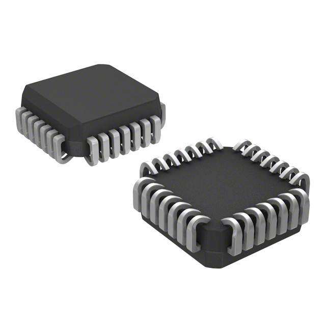
| 描述 | IC PWR I/F SWITCH PC CARD 16SSOP电源开关 IC - 配电 1A Sngl-Slot PC Card Power Switch |
| 产品分类 | PMIC - 电源分配开关开关 IC |
| 品牌 | Texas Instruments |
| 产品手册 | |
| 产品图片 |
|
| rohs | 符合RoHS无铅 / 符合限制有害物质指令(RoHS)规范要求 |
| 产品系列 | 电源开关 IC - 配电,Texas Instruments TPS2211IDB- |
| 数据手册 | |
| 产品型号 | TPS2211IDB |
| Rds(On) | 50 毫欧 |
| 产品 | PCI Power Management |
| 产品种类 | 电源开关 IC - 配电 |
| 供应商器件封装 | 16-SSOP |
| 其它名称 | 296-26919-5 |
| 内部开关 | 是 |
| 包装 | 管件 |
| 单位重量 | 128.600 mg |
| 商标 | Texas Instruments |
| 安装类型 | 表面贴装 |
| 安装风格 | SMD/SMT |
| 导通电阻—最大值 | 50 mOhms |
| 封装 | Tube |
| 封装/外壳 | 16-SSOP(0.209",5.30mm 宽) |
| 封装/箱体 | SSOP-16 |
| 工作温度 | -40°C ~ 85°C |
| 工厂包装数量 | 80 |
| 开关数量 | 1 Switch |
| 开关类型 | PCMCIA 个开关 |
| 最大输入电压 | 12 V |
| 最小输入电压 | 3.3 V |
| 标准包装 | 80 |
| 比率-输入:输出 | 3:2 |
| 特性 | - |
| 电压-负载 | 3.3V, 5V, 12V |
| 电压-输入 | 3.3V,5V,12V |
| 电流-输出(最大值) | 1A |
| 电流限制 | 1 A |
| 类型 | PCMCIA/Cardbus Switch Matrix |
| 系列 | TPS2211 |
| 输入类型 | - |
| 输出数 | 2 |
| 输出端数量 | 1 Output |
| 输出类型 | - |


- 商务部:美国ITC正式对集成电路等产品启动337调查
- 曝三星4nm工艺存在良率问题 高通将骁龙8 Gen1或转产台积电
- 太阳诱电将投资9.5亿元在常州建新厂生产MLCC 预计2023年完工
- 英特尔发布欧洲新工厂建设计划 深化IDM 2.0 战略
- 台积电先进制程称霸业界 有大客户加持明年业绩稳了
- 达到5530亿美元!SIA预计今年全球半导体销售额将创下新高
- 英特尔拟将自动驾驶子公司Mobileye上市 估值或超500亿美元
- 三星加码芯片和SET,合并消费电子和移动部门,撤换高东真等 CEO
- 三星电子宣布重大人事变动 还合并消费电子和移动部门
- 海关总署:前11个月进口集成电路产品价值2.52万亿元 增长14.8%


PDF Datasheet 数据手册内容提取
TPS2211 SINGLE-SLOT PC CARD POWER INTERFACE SWITCH FOR PARALLEL PCMCIA CONTROLLERS SLVS156E – JULY 1997 – REVISED JANUARY 2001 (cid:0) Fully Integrated VCC and Vpp Switching for DB PACKAGE (TOP VIEW) Single-Slot PC Card Interface (cid:0) Low r (90-mΩ 5-V V Switch and VCCD0 1 16 SHDN DS(on) CC VCCD1 2 15 VPPD0 3.3-V V Switch) CC 3.3V 3 14 VPPD1 (cid:0) Compatible With Controllers From Cirrus, 3.3V 4 13 AVCC Ricoh, O Micro, Intel, and Texas 5V 5 12 AVCC 2 Instruments 5V 6 11 AVCC (cid:0) GND 7 10 AVPP 3.3-V Low-Voltage Mode OC 8 9 12V (cid:0) Meets PC Card Standards (cid:0) 12-V Supply Can Be Disabled Except During 12-V Flash Programming (cid:0) Short-Circuit and Thermal Protection (cid:0) Space-Saving 16-Pin SSOP (DB) (cid:0) Compatible With 3.3-V, 5-V, and 12-V PC Cards (cid:0) Break-Before-Make Switching description The TPS2211 PC Card power-interface switch provides an integrated power-management solution for a single PC Card. All of the discrete power MOSFETs, a logic section, current limiting, and thermal protection for PC Card control are combined on a single integrated circuit, using the Texas Instruments LinBiCMOS process. The circuit allows the distribution of 3.3-V, 5-V, and/or 12-V card power, and is compatible with many PCMCIA controllers. The current-limiting feature eliminates the need for fuses, which reduces component count and improves reliability. Current-limit reporting can help the user isolate a system fault to the PC Card. The TPS2211 features a 3.3-V low-voltage mode that allows for 3.3-V switching without the need for 5 V. Bias power can be derived from either the 3.3-V or 5-V inputs. This facilitates low-power system designs such as sleep mode and pager mode where only 3.3 V is available. End equipment for the TPS2211 includes notebook computers, desktop computers, personal digital assistants (PDAs), digital cameras, and bar-code scanners. AVAILABLE OPTIONS PACKAGED DEVICE CCHHIIPP FFOORRMM TA SMALL OUTLINE (Y) (DB) –40°C to 85°C TPS2211IDBR TPS2211Y The DB package is only available taped and reeled, indicated by the R suffix on the device type. Please be aware that an important notice concerning availability, standard warranty, and use in critical applications of TexasInstruments semiconductor products and disclaimers thereto appears at the end of this data sheet. PC Card is a trademark of PCMCIA (Personal Computer Memory Card International Association). LinBiCMOS is a trademark of Texas Instruments Incorporated. PRODUCTION DATA information is current as of publication date. Copyright 2001, Texas Instruments Incorporated Products conform to specifications per the terms of Texas Instruments standard warranty. Production processing does not necessarily include testing of all parameters. POST OFFICE BOX 655303 • DALLAS, TEXAS 75265 1
TPS2211 SINGLE-SLOT PC CARD POWER INTERFACE SWITCH FOR PARALLEL PCMCIA CONTROLLERS SLVS156E – JULY 1997 – REVISED JANUARY 2001 typical PC-card power-distribution application TPS2211 AVCC AVCC AVCC VCC1 0.1 µF VCC2 PC Card Vpp1 Connector AVPP Vpp2 12 V 12V 0.1 µF 5 V 5V 0.1 µF 1 µF 5V PCMCIA Controller 3.3 V 3.3V VCCD0 VCC_EN0 0.1 µF 1 µF 3.3V VCCD1 VCC_EN1 VPPD0 VPP_EN0 VPPD1 VPP_EN1 OC To CPU CS GND SHDN Shutdown Signal From CPU 2 POST OFFICE BOX 655303 • DALLAS, TEXAS 75265
TPS2211 SINGLE-SLOT PC CARD POWER INTERFACE SWITCH FOR PARALLEL PCMCIA CONTROLLERS SLVS156E – JULY 1997 – REVISED JANUARY 2001 TPS2211Y chip information This chip, when properly assembled, displays characteristics similar to those of the TPS2211. Thermal compression or ultrasonic bonding may be used on the doped-aluminum bonding pads. The chips may be mounted with conductive epoxy or a gold-silicon preform. BONDING PAD ASSIGNMENTS 2 1 16 15 14 VCCD0 1 16 SHDN VCCD1 2 15 VPPD0 13 3.3V 3 14 VPPD1 3.3V 4 13 AVCC TPS2211Y 3 5V 5 12 AVCC 5V 6 11 AVCC 4 GND 7 10 AVPP OC 8 9 12V 13 140 12 CHIP THICKNESS: 15 TYPICAL BONDING PADS: 4 × 4 MINIMUM 5 TJmax = 150°C TOLERANCES ARE ±10%. 6 ALL DIMENSIONS ARE IN MILS. 11 7 10 8 9 77 POST OFFICE BOX 655303 • DALLAS, TEXAS 75265 3
TPS2211 SINGLE-SLOT PC CARD POWER INTERFACE SWITCH FOR PARALLEL PCMCIA CONTROLLERS SLVS156E – JULY 1997 – REVISED JANUARY 2001 Terminal Functions TERMINAL II//OO DDEESSCCRRIIPPTTIIOONN NAME NO. 3.3V 3, 4 I 3.3-V VCC input for card power and/or chip power if 5 V is not present 5V 5, 6 I 5-V VCC input for card power and/or chip power 12V 9 I 12-V Vpp input card power AVCC 11, 12, 13 O Switched output that delivers 0 V, 3.3-V, 5-V, or high impedance to card AVPP 10 O Switched output that delivers 0 V 3.3-V, 5-V, 12-V, or high impedance to card GND 7 Ground OC 8 O Logic-level overcurrent reporting output that goes low when an overcurrent conditions exists SHDN 16 I Logic input that shuts down the TPS2211 and sets all power outputs to high-impedance state VCCD0 1 I Logic input that controls voltage of AVCC (see control-logic table) VCCD1 2 I Logic input that controls voltage of AVCC (see control-logic table) VPPD0 15 I Logic input that controls voltage of AVPP (see control-logic table) VPPD1 14 I Logic input that controls voltage of AVPP (see control-logic table) absolute maximum ratings over operating free-air temperature (unless otherwise noted)† Input voltage range for card power: V . . . . . . . . . . . . . . . . . . . . . . . . . . . . . . . . . . . . . . . . . . . –0.3 V to 7 V I(5V) V . . . . . . . . . . . . . . . . . . . . . . . . . . . . . . . . . . . . . . . . . –0.3 V to 7 V I(3.3V) V . . . . . . . . . . . . . . . . . . . . . . . . . . . . . . . . . . . . . . . . . –0.3 V to 14 V I(12V) Logic input voltage . . . . . . . . . . . . . . . . . . . . . . . . . . . . . . . . . . . . . . . . . . . . . . . . . . . . . . . . . . . . . . . . . –0.3 V to 7 V Continuous total power dissipation . . . . . . . . . . . . . . . . . . . . . . . . . . . . . . . . . . . . . See Dissipation Rating Table Output current (each card): I . . . . . . . . . . . . . . . . . . . . . . . . . . . . . . . . . . . . . . . . . . . . . . internally limited O(VCC) I . . . . . . . . . . . . . . . . . . . . . . . . . . . . . . . . . . . . . . . . . . . . . . internally limited O(VPP) Operating virtual junction temperature range, TJ . . . . . . . . . . . . . . . . . . . . . . . . . . . . . . . . . . . . . –40°C to 150°C Operating free-air temperature range, T . . . . . . . . . . . . . . . . . . . . . . . . . . . . . . . . . . . . . . . . . . . . –40°C to 85°C A Storage temperature range, T . . . . . . . . . . . . . . . . . . . . . . . . . . . . . . . . . . . . . . . . . . . . . . . . . . . –55°C to 150°C stg Lead temperature 1.6 mm (1/16 inch) from case for 10 seconds . . . . . . . . . . . . . . . . . . . . . . . . . . . . . . . 260°C †Stresses beyond those listed under “absolute maximum ratings” may cause permanent damage to the device. These are stress ratings only, and functional operation of the device at these or any other conditions beyond those indicated under “recommended operating conditions” is not implied. Exposure to absolute-maximum-rated conditions for extended periods may affect device reliability. DISSIPATION RATING TABLE TA ≤ 25°C DERATING FACTOR TA = 70°C TA = 85°C PACKAGE POWER RATING ABOVE TA = 25°C POWER RATING POWER RATING DB 775 mW 6.2 mW/°C 496 mW 403 mW These devices are mounted on an FR4 board with no special thermal considerations. recommended operating conditions MIN MAX UNIT VI(5V) 0 5.25 V Input voltage, VI VI(3.3V) 0 5.25 V VI(12V) 0 13.5 V IO(AVCC) 1 A OOuuttppuutt ccuurrrreenntt IO(AVPP) 150 mA Operating virtual junction temperature, TJ –40 125 °C 4 POST OFFICE BOX 655303 • DALLAS, TEXAS 75265
TPS2211 SINGLE-SLOT PC CARD POWER INTERFACE SWITCH FOR PARALLEL PCMCIA CONTROLLERS SLVS156E – JULY 1997 – REVISED JANUARY 2001 electrical characteristics, T = –40°C to 85°C (unless otherwise noted) A power switch TPS2211 PPAARRAAMMEETTEERR TTEESSTT CCOONNDDIITTIIOONNSS†† UUNNIITT MIN TYP MAX 5 V to AVCC VI(5V) = 5 V 50 90 3.3 V to AVCC VI(5V) = 5 V, VI(3.3V) = 3.3 V 48 90 mΩ 3.3 V to AVCC VI(5V) = 0 V, VI(3.3V) = 3.3 V 48 90 SSwwiittcchh rreessiissttaannccee 5 V to AVPP TJ=25°C 6 3.3 V to AVPP TJ=25°C 6 Ω 12 V to AVPP TJ=25°C 1 VO(AVPP) Clamp low voltage Ipp at 10 mA 0.8 V VO(AVCC) Clamp low voltage ICC at 10 mA 0.8 V TA = 25°C 1 10 IIpp hhiigghh-iimmppeeddaannccee ssttaattee TA= 85°C 50 IIllkkg LLeeaakkaaggee ccuurrrreenntt µµAA TA = 25°C 1 10 IICCCC hhiigghh-iimmppeeddaannccee ssttaattee TA=85°C 50 VI(5V) = 5 V VO(AVCC) = 5 V, VO(AVPP) = 12 V 40 150 II Input current VVII((35.V3)V =) =0 3V.,3 V VO(AVCC) = 3.3 V, VO(AVPP) = 12 V 40 150 µA Shutdown mode VO(AVCC) = VO(AVPP) = Hi-Z 1 Short-circuit IO(AVCC) TJJ = 85°C, output powered into a 1 2.2 A IIOOSS output-current limit IO(AVPP) short to GND 120 400 mA †Pulse-testing techniques maintain junction temperature close to ambient temperature; thermal effects must be taken into account separately. logic section TPS2211 PPAARRAAMMEETTEERR TTEESSTT CCOONNDDIITTIIOONNSS†† UUNNIITT MIN MAX Logic input current 1 µA Logic input high level 2 V Logic input low level 0.8 V VI(5V) = 5 V, IO = 1 mA VI(5V) – 0.4 LLooggiicc oouuttppuutt hhiigghh lleevveell VV VI(5V) = 0 V, IO = 1 mA, VI(3.3V) = 3.3 V VI(3.3V) – 0.4 Logic output low level IO = 1 mA 0.4 V †Pulse-testing techniques maintain junction temperature close to ambient temperature; thermal effects must be taken into account separately. POST OFFICE BOX 655303 • DALLAS, TEXAS 75265 5
TPS2211 SINGLE-SLOT PC CARD POWER INTERFACE SWITCH FOR PARALLEL PCMCIA CONTROLLERS SLVS156E – JULY 1997 – REVISED JANUARY 2001 electrical characteristics, T = 25°C (unless otherwise noted) A power switch TPS2211Y PPAARRAAMMEETTEERR TTEESSTT CCOONNDDIITTIIOONNSS†† UUNNIITT MIN TYP MAX 5 V to AVCC VI(5V) = 5 V 50 3.3 V to AVCC VI(5V) = 5 V, VI(3.3V) = 3.3 V 48 mΩ 3.3 V to AVCC VI(5V) = 0 V, VI(3.3V) = 3.3 V 48 SSwwiittcchh rreessiissttaannccee 5 V to AVPP TJ=25°C 4.3 3.3 V to AVPP TJ=25°C 4.3 Ω 12 V to AVPP TJ=25°C 0.5 VO(AVPP) Clamp low voltage Ipp at 10 mA 0.28 V VO(AVCC) Clamp low voltage Ipp at 10 mA 0.28 V Ipp high-impedance state 1 IIllkkg LLeeaakkaaggee ccuurrrreenntt µµAA ICC high-impedance state 1 VI = 5 V VO(AVCC) = 5 V, VO(AVPP) = 12 V 42 II Input current VI(5V) = 5 V, µA VI(3.3V) = 3.3 V VO(AVCC) = 3.3 V, VO(AVPP) = 12 V 42 †Pulse-testing techniques maintain junction temperature close to ambient temperature; thermal effects must be taken into account separately. switching characteristics‡ TPS2211, PARAMETER TEST CONDITIONS§ TPS2211Y UNIT MIN TYP MAX VO(AVCC) 2.8 ttr RRiissee ttiimmeess, oouuttppuutt VO(AVPP) 6.4 mmss VO(AVCC) 4.5 ttff FFaallll ttiimmeess, oouuttppuutt VO(AVPP) 12 ton 6.8 VVII((VVPPPPDD00)) ttoo VVOO((AAVVPPPP)) toff 18 ton 4 ttpdd PPrrooppaaggaattiioonn ddeellaayy ((sseeee FFiigguurree11)) VVII((VVCCCCDD11)) ttoo VVOO((AAVVCCCC)) ((33.33VV)) mmss toff 17 ton 6.6 VVII((VVCCCCDD00)) ttoo VVOO((AAVVCCCC)) ((55VV)) toff 17 ‡Switching Characteristics are with CL = 150 µF. §Refer to Parameter Measurement Information 6 POST OFFICE BOX 655303 • DALLAS, TEXAS 75265
TPS2211 SINGLE-SLOT PC CARD POWER INTERFACE SWITCH FOR PARALLEL PCMCIA CONTROLLERS SLVS156E – JULY 1997 – REVISED JANUARY 2001 PARAMETER MEASUREMENT INFORMATION AVPP AVCC CL CL LOAD CIRCUIT LOAD CIRCUIT VI(VPPD0) VDD VI(VCCD1) VDD 50% 50% 50% 50% (VI(VPPD1) = 0 V) (VI(VCCD0) = VDD) GND GND toff toff ton ton VO(AVPP) 90% VI(12V) VO(AVCC) 90% VI(3.3V) 10% 10% GND GND VOLTAGE WAVEFORMS VOLTAGE WAVEFORMS Figure 1. Test Circuits and Voltage Waveforms Table of Timing Diagrams FIGURE AVCC Propagation Delay and Rise Time With 1-µF Load, 3.3-V Switch 2 AVCC Propagation Delay and Fall Time With 1-µF Load, 3.3-V Switch 3 AVCC Propagation Delay and Rise Time With 150-µF Load, 3.3-V Switch 4 AVCC Propagation Delay and Fall Time With 150-µF Load, 3.3-V Switch 5 AVCC Propagation Delay and Rise Time With 1-µF Load, 5-V Switch 6 AVCC Propagation Delay and Fall Time With 1-µF Load, 5-V Switch 7 AVCC Propagation Delay and Rise Time With 150-µF Load, 5-V Switch 8 AVCC Propagation Delay and Fall Time With 150-µF Load, 5-V Switch 9 AVPP Propagation Delay and Rise Time With 1-µF Load, 12-V Switch 10 AVPP Propagation Delay and Fall Time With 1-µF Load, 12-V Switch 11 AVPP Propagation Delay and Rise Time With 150-µF Load, 12-V Switch 12 AVPP Propagation Delay and Fall Time With 150-µF Load, 12-V Switch 13 POST OFFICE BOX 655303 • DALLAS, TEXAS 75265 7
TPS2211 SINGLE-SLOT PC CARD POWER INTERFACE SWITCH FOR PARALLEL PCMCIA CONTROLLERS SLVS156E – JULY 1997 – REVISED JANUARY 2001 PARAMETER MEASUREMENT INFORMATION VCCD0 = 3.3 V VCCD0 = 3.3 V VCCD1 VCCD1 (2 V/div) (2 V/div) AVCC AVCC (2 V/div) (2 V/div) 0 1 2 3 4 5 6 7 8 9 0 5 10 15 20 25 30 35 40 45 t – Time – ms t – Time – ms Figure 2. AVCC Propagation Delay and Rise Time Figure 3. AVCC Propagation Delay and Fall Time With 1-µF Load, 3.3-V Switch With 1-µF Load, 3.3-V Switch VCCD0 = 3.3 V VCCD0 = 3.3 V VCCD1 VCCD1 (2 V/div) (2 V/div) AVCC AVCC (2 V/div) (2 V/div) 0 1 2 3 4 5 6 7 8 9 0 5 10 15 20 25 30 35 40 45 t – Time – ms t – Time – ms Figure 4. AVCC Propagation Delay and Rise Time Figure 5. AVCC Propagation Delay and Fall Time With 150-µF Load, 3.3-V Switch With 150-µF Load, 3.3-V Switch 8 POST OFFICE BOX 655303 • DALLAS, TEXAS 75265
TPS2211 SINGLE-SLOT PC CARD POWER INTERFACE SWITCH FOR PARALLEL PCMCIA CONTROLLERS SLVS156E – JULY 1997 – REVISED JANUARY 2001 PARAMETER MEASUREMENT INFORMATION VCCD0 VCCD0 (2 V/div) (2 V/div) AVCC AVCC (2 V/div) VCCD1 = 5 V (2 V/div) VCCD1 = 5 V 0 2 4 6 8 10 12 14 16 18 0 5 10 15 20 25 30 35 40 45 t – Time – ms t – Time – ms Figure 6. AVCC Propagation Delay and Rise Time Figure 7. AVCC Propagation Delay and Fall Time With 1-µF Load, 5-V Switch With 1-µF Load, 5-V Switch VCCD0 VCCD0 (2 V/div) (2 V/div) AVCC AVCC (2 V/div) (2 V/div) VCCD1 = 5 V VCCD1 = 5 V 0 2 4 6 8 10 12 14 16 18 0 5 10 15 20 25 30 35 40 45 t – Time – ms t – Time – ms Figure 8. AVCC Propagation Delay and Rise Time Figure 9. AVCC Propagation Delay and Fall Time With 150-µF Load, 5-V Switch With 150-µF Load, 5-V Switch POST OFFICE BOX 655303 • DALLAS, TEXAS 75265 9
TPS2211 SINGLE-SLOT PC CARD POWER INTERFACE SWITCH FOR PARALLEL PCMCIA CONTROLLERS SLVS156E – JULY 1997 – REVISED JANUARY 2001 PARAMETER MEASUREMENT INFORMATION VPPD1 = 0 V VPPD0 VPPD0 (2 V/div) (2 V/div) AVPP AVPP (5 V/div) (5 V/div) VPPD1 = 0 V 0 0.2 0.4 0.6 0.8 1 1.2 1.4 1.6 1.8 0 1 2 3 4 5 6 7 8 9 t – Time – ms t – Time – ms Figure 10. AVPP Propagation Delay and Rise Time Figure 11. AVPP Propagation Delay and Fall Time With 1-µF Load, 12-V Switch With 1-µF Load, 12-V Switch VPPD1 = 0 V VPPD0 VPPD0 (2 V/div) (2 V/div) AVPP AVPP (5 V/div) (5 V/div) VPPD1 = 0 V 0 2 4 6 8 10 12 14 16 18 0 5 10 15 20 25 30 35 40 45 t – Time – ms t – Time – ms Figure 12. AVPP Propagation Delay and Rise Time Figure 13. AVPP Propagation Delay and Fall Time With 150-µF Load, 12-V Switch With 150-µF Load, 12-V Switch 10 POST OFFICE BOX 655303 • DALLAS, TEXAS 75265
TPS2211 SINGLE-SLOT PC CARD POWER INTERFACE SWITCH FOR PARALLEL PCMCIA CONTROLLERS SLVS156E – JULY 1997 – REVISED JANUARY 2001 TYPICAL CHARACTERISTICS Table of Graphs FIGURE ICC(5V) Supply current vs Junction temperature 14 ICC(3.3V) Supply current vs Junction temperature 15 rDS(on) Static drain-source on-state resistance, 5-V VCC switch vs Junction temperature 16 rDS(on) Static drain-source on-state resistance, 3.3-V VCC switch vs Junction temperature 17 rDS(on) Static drain-source on-state resistance, 12-V VPP switch vs Junction temperature 18 VO(AVCC) Output voltage, 5-V VCC switch vs Output current 19 VO(AVCC) Output voltage, 3.3-V VCC switch vs Output current 20 VO(AVPP) Output voltage, 12-V VPP switch vs Output current 21 IOS(AVCC) Short-circuit current, 5-V VCC switch vs Junction temperature 22 IOS(AVCC) Short-circuit current, 3.3-V VCC switch vs Junction temperature 23 IOS(AVPP) Short-circuit current, 12-V VPP switch vs Junction temperature 24 SUPPLY CURRENT SUPPLY CURRENT vs vs JUNCTION TEMPERATURE JUNCTION TEMPERATURE 45 45 VO(AVCC) = 5 V VO(AVCC) = 3.3 V VO(AVPP) = 12 V VO(AVPP) = 12 V No Load No Load 43 43 A A µ µ Current – 41 Current – 41 Supply 39 Supply 39 – – C C C C I 37 I 37 35 35 –50 –25 0 25 50 75 100 125 –50 –25 0 25 50 75 100 125 TJ – Junction Temperature – °C TJ – Junction Temperature – °C Figure 14 Figure 15 POST OFFICE BOX 655303 • DALLAS, TEXAS 75265 11
TPS2211 SINGLE-SLOT PC CARD POWER INTERFACE SWITCH FOR PARALLEL PCMCIA CONTROLLERS SLVS156E – JULY 1997 – REVISED JANUARY 2001 TYPICAL CHARACTERISTICS 5-V VCC SWITCH 3.3-V VCC SWITCH STATIC DRAIN-SOURCE ON-STATE RESISTANCE STATIC DRAIN-SOURCE ON-STATE RESISTANCE vs vs JUNCTION TEMPERATURE JUNCTION TEMPERATURE Ω Ω m m e – 110 VI(5V) e – 90 VI(3.3V) = 3.3 V nc VI(AVCC) = 5 V nc VI(AVCC) = 3.3 V a 100 a st st si si 80 e e R R e 90 e at at St St On- 80 On- 70 e e c c r r u u o 70 o S S 60 n- n- ai ai Dr 60 Dr c c ati ati 50 St 50 St – – n) n) o o S( 40 S( 40 D –50 –25 0 25 50 75 100 125 D –50 –25 0 25 50 75 100 125 r r TJ – Junction Temperature – °C TJ – Junction Temperature – °C Figure 16 Figure 17 12-V VPP SWITCH 5-V VCC SWITCH STATIC DRAIN-SOURCE ON-STATE RESISTANCE OUTPUT VOLTAGE vs vs JUNCTION TEMPERATURE OUTPUT CURRENT Ω m e – 1200 VI(5V) = 5 V 5 nc VI(AVPP) = 12 V –40°C a st 1100 4.98 esi V 25°C R – e e n-Stat 1000 Voltag 4.96 ce O 900 put 4.94 85°C ur ut o O 125°C S – Drain- 800 VCC) 4.92 Static 700 VO(A 4.9 – n) o S( 600 4.88 D –50 –25 0 25 50 75 100 125 0 0.2 0.4 0.6 0.8 1 r TJ – Junction Temperature – °C IO(AVCC) – Output Current – A Figure 18 Figure 19 12 POST OFFICE BOX 655303 • DALLAS, TEXAS 75265
TPS2211 SINGLE-SLOT PC CARD POWER INTERFACE SWITCH FOR PARALLEL PCMCIA CONTROLLERS SLVS156E – JULY 1997 – REVISED JANUARY 2001 TYPICAL CHARACTERISTICS 3.3-V VCC SWITCH 12-V VPP SWITCH OUTPUT VOLTAGE OUTPUT VOLTAGE vs vs OUTPUT CURRENT OUTPUT CURRENT 3.3 12 –40°C 11.98 –40°C 3.28 e – V 25°C e – V 11.96 25°C g g a a Volt 3.26 Volt 11.94 ut ut utp 85°C utp 11.92 O O – C) 3.24 125°C – P) 11.9 85°C C P O(AV O(AV 11.88 125°C V 3.22 V 11.86 3.2 11.84 0 0.2 0.4 0.6 0.8 1 0 0.03 0.06 0.09 0.12 IO(AVCC) – Output Current – A IO(AVPP) – Output Current – A Figure 20 Figure 21 5-V VCC SWITCH 3.3-V VCC SWITCH SHORT-CIRCUIT CURRENT SHORT-CIRCUIT CURRENT vs vs JUNCTION TEMPERATURE JUNCTION TEMPERATURE 1.8 1.7 A A – 1.6 – 1.65 nt nt e e r 1.4 r 1.6 r r u u C C ut 1.2 ut 1.55 p p ut ut O 1 O 1.5 uit uit c c Cir 0.8 Cir 1.45 rt- rt- o 0.6 o 1.4 h h S S – – C) 0.4 C) 1.35 C C V V A A S( 0.2 S( 1.3 O O I I 0 1.25 –50 –25 0 25 50 75 100 125 –50 –25 0 25 50 75 100 125 TJ – Junction Temperature – °C TJ – Junction Temperature – °C Figure 22 Figure 23 POST OFFICE BOX 655303 • DALLAS, TEXAS 75265 13
TPS2211 SINGLE-SLOT PC CARD POWER INTERFACE SWITCH FOR PARALLEL PCMCIA CONTROLLERS SLVS156E – JULY 1997 – REVISED JANUARY 2001 TYPICAL CHARACTERISTICS 12-V VPP SWITCH SHORT-CIRCUIT CURRENT vs JUNCTION TEMPERATURE 0.28 A – nt e 0.26 r r u C ut p ut 0.24 O uit c r Ci rt- 0.22 o h S – P) P 0.2 V A S( O I 0.18 –50 –25 0 25 50 75 100 125 TJ – Junction Temperature – °C Figure 24 APPLICATION INFORMATION overview PC Cards were initially introduced as a means to add EEPROM (flash memory) to portable computers with limited onboard memory. The idea of add-in cards quickly took hold; modems, wireless LANs, GPS systems, multimedia, and hard-disk versions were soon available. As the number of PC Card applications grew, the engineering community quickly recognized the need for a standard to ensure compatibility across platforms. To this end, the PCMCIA (Personal Computer Memory Card International Association) was established, comprised of members from leading computer, software, PC Card, and semiconductor manufacturers. One key goal was to realize the plug-and-play concept, i.e. cards and hosts from different vendors should be compatible. PC Card power specification System compatibility also means power compatibility. The most current set of specifications (PC Card Standard) set forth by the PCMCIA committee states that power is to be transferred between the host and the card through eight of the 68 terminals of the PC Card connectors. This power interface consists of two V , two V , and four CC pp ground terminals. Multiple V and ground terminals minimize connector-terminal and line resistance. The two CC V terminals were originally specified as separate signals but are commonly tied together in the host to form pp a single node to minimize voltage losses. Card primary power is supplied through the V terminals; flash- CC memory programming and erase voltage is supplied through the V terminals. pp 14 POST OFFICE BOX 655303 • DALLAS, TEXAS 75265
TPS2211 SINGLE-SLOT PC CARD POWER INTERFACE SWITCH FOR PARALLEL PCMCIA CONTROLLERS SLVS156E – JULY 1997 – REVISED JANUARY 2001 APPLICATION INFORMATION designing for voltage regulation The current PCMCIA specification for output voltage regulation of the 5-V output is 5% (250 mV). In a typical PC power-system design, the power supply will have an output voltage regulation (V ) of 2% (100 mV). PS(reg) Also, a voltage drop from the power supply to the PC Card will result from resistive losses (V ) in the PCB PCB traces and the PCMCIA connector. A typical design would limit the total of these resistive losses to less than 1% (50 mV) of the output voltage. Therefore, the allowable voltage drop (V ) for the TPS2211 is the PCMCIA DS voltage regulation less the power supply regulation and less the PCB and connector resistive drops: VDS (cid:0) VO(cid:1)reg(cid:2) – VPS(cid:1)reg(cid:2) – VPCB Typically, this would leave 100 mV for the allowable voltage drop across the TPS2211. The voltage drop is the output current multiplied by the switch resistance of the TPS2211. Therefore, the maximum output current that can be delivered to the PC Card in regulation is the allowable voltage drop across the TPS2211 divided by the output switch resistance. V DS IOmax (cid:0) r DS(cid:1)on(cid:2) The AVCC outputs deliver 1 A continuous at 5 V and 3.3 V within regulation over the operating temperature range. Using the same equations, the PCMCIA specification for output voltage regulation of the 3.3-V output is 300 mV. Using the voltage drop percentages for power supply regulation (2%) and PCB resistive loss (1%), the allowable voltage drop for the 3.3-V switch is 200 mV. The 12-V outputs (AVPP) of the TPS2211 can deliver 150 mA continuously. overcurrent and overtemperature protection PC Cards are inherently subject to damage from mishandling. Host systems require protection against short-circuited cards that could lead to power supply or PCB trace damage. Even systems sufficiently robust to withstand a short circuit would still undergo rapid battery discharge into the damaged PC Card, resulting in a sudden loss of system power. Most hosts include fuses for protection. The reliability of fused systems is poor and requires troubleshooting and repair, usually by the manufacturer, when fuses are blown. The TPS2211 uses sense FETs to check for overcurrent conditions in each of the AVCC and AVPP outputs. Unlike sense resistors or polyfuses, these FETs do not add to the series resistance of the switch; therefore voltage and power losses are reduced. Overcurrent sensing is applied to each output separately. When an overcurrent condition is detected, only the power output affected is limited; all other power outputs continue to function normally. The OC indicator, normally a logic high, is a logic low when an overcurrent condition is detected providing for initiation of system diagnostics and/or sending a warning message to the user. During power up, the TPS2211 controls the rise time of the AVCC and AVPP outputs and limits the current into a faulty card or connector. If a short circuit is applied after power is established (e.g., hot insertion of a bad card), current is initially limited only by the impedance between the short and the power supply. In extreme cases, as much as 10 A to 15 A may flow into the short before the current limiting of the TPS2211 engages. If the AVCC or AVPP outputs are driven below ground, the TPS2211 may latch nondestructively in an off state. Cycling power will reestablish normal operation. Overcurrent limiting for the AVCC outputs is designed to activate if powered up into a short in the range of 1 A to 2.2 A, typically at about 1.6 A. The AVPP outputs limit from 120 mA to 400 mA, typically around 280 mA. The protection circuitry acts by linearly limiting the current passing through the switch rather than initiating a full shutdown of the supply. Shutdown occurs only during thermal limiting. Thermal limiting prevents destruction of the IC from overheating if the package power dissipation ratings are exceeded. Thermal limiting disables power output until the device has cooled. POST OFFICE BOX 655303 • DALLAS, TEXAS 75265 15
TPS2211 SINGLE-SLOT PC CARD POWER INTERFACE SWITCH FOR PARALLEL PCMCIA CONTROLLERS SLVS156E – JULY 1997 – REVISED JANUARY 2001 APPLICATION INFORMATION 12-V supply not required Most PC Card switches use the externally supplied 12 V to power gate drive and other chip functions, which require that power be present at all times. The TPS2211 offers considerable power savings by using an internal charge pump to generate the required higher voltages from the 5-V input. Therefore, the external 12-V supply can be disabled except when needed for flash-memory functions, thereby extending battery lifetime. Do not ground the 12-V switch inputs when the 12-V input is not used. Additional power savings are realized by the TPS2211 during a software shutdown in which quiescent current drops to a maximum of 1 µA. 3.3-V low-voltage mode The TPS2211 will operate in a 3.3-V low-voltage mode when 3.3 V is the only available input voltage (V = 0). This allows host and PC Cards to be operated in low-power 3.3-volts-only modes such as sleep or I(5V) pager modes. Note that in these operation modes, the TPS2211 will derive its bias current from the 3.3-V input pin and only 3.3 V can be delivered to the PC Card. voltage transitioning requirement PC Cards are migrating from 5 V to 3.3 V to minimize power consumption, optimize board space, and increase logic speeds. The TPS2211 meets all combinations of power delivery as currently defined in the PCMCIA standard. The latest protocol accommodates mixed 3.3-V/5-V systems by first powering the card with 5 V, then polling it to determine its 3.3-V compatibility. The PCMCIA specification requires that the capacitors on 3.3-V compatible cards be discharged to below 0.8 V before applying 3.3-V power. This functions as a power reset and ensures that sensitive 3.3-V circuitry is not subjected to any residual 5-V charge. The TPS2211 offers a selectable V and V ground state, in accordance with PCMCIA 3.3-V/5-V switching specifications. CC pp output ground switches PC Card specification requires that V be discharged within 100 ms. PC Card resistance can not be relied on CC to provide a discharge path for voltages stored on PC Card capacitance because of possible high-impedance isolation by power-management schemes. power-supply considerations The TPS2211 has multiple pins for each of its 3.3-V and 5-V power inputs and for the switched AVCC outputs. Any individual pin can conduct the rated input or output current. Unless all pins are connected in parallel, the series resistance is significantly higher than that specified, resulting in increased voltage drops and lost power. It is recommended that all input and output power pins be paralleled for optimum operation. To increase the noise immunity of the TPS2211, the power supply inputs should be bypassed with a 1-µF electrolytic or tantalum capacitor paralleled by a 0.047-µF to 0.1-µF ceramic capacitor. It is strongly recommended that the switched outputs be bypassed with a 0.1-µF, or larger, ceramic capacitor; doing so improves the immunity of the TPS2211 to electrostatic discharge (ESD). Care should be taken to minimize the inductance of PCB traces between the TPS2211 and the load. High switching currents can produce large negative voltage transients, which forward biases substrate diodes, resulting in unpredictable performance. Similarly, no pin should be taken below –0.3 V. 16 POST OFFICE BOX 655303 • DALLAS, TEXAS 75265
TPS2211 SINGLE-SLOT PC CARD POWER INTERFACE SWITCH FOR PARALLEL PCMCIA CONTROLLERS SLVS156E – JULY 1997 – REVISED JANUARY 2001 APPLICATION INFORMATION calculating junction temperature The switch resistance, r , is dependent on the junction temperature, T , of the die and the current through DS(on) J the switch. To calculate T , first find r from Figures 16 through 18 using an initial temperature estimate J DS(on) about 50°C above ambient. Then calculate the power dissipation for each switch, using the formula: PD (cid:2) rDS(cid:4)on(cid:5) (cid:0) I2 Next, sum the power dissipation and calculate the junction temperature: TJ (cid:2) (cid:4)(cid:6)PD (cid:0) R(cid:0)JA(cid:5) (cid:1) TA, R(cid:0)JA (cid:2) 108°C(cid:3)W Compare the calculated junction temperature with the initial temperature estimate. If the temperatures are not within a few degrees of each other, recalculate using the calculated temperature as the initial estimate. ESD protection All TPS2211 inputs and outputs incorporate ESD-protection circuitry designed to withstand a 2-kV human-body- model discharge as defined in MIL-STD-883C, Method 3015. The AVCC and AVPP outputs can be exposed to potentially higher discharges from the external environment through the PC Card connector. Bypassing the out- puts with 0.1-µF capacitors protects the devices from discharges up to 10 kV. TPS2211 Card B 3 S1 13 17 3.3 V CS VCC1 3.3 V 4 S2 12 51 VCC2 11 5 S3 5 V S4 6 5 V S5 18 9 S6 10 52 Vpp1 12 V CS Vpp2 See Note A Internal Current Monitor 16 CPU SHDN Thermal 15 VPPD0 14 VPPD1 1 Controller VCCD0 2 VCCD1 8 GND OC 7 NOTE A: MOSFET switch S6 has a back-gate diode from the source to the drain. Unused switch inputs should never be grounded. Figure 25. Internal Switching Matrix, TPS2211 Control Logic POST OFFICE BOX 655303 • DALLAS, TEXAS 75265 17
TPS2211 SINGLE-SLOT PC CARD POWER INTERFACE SWITCH FOR PARALLEL PCMCIA CONTROLLERS SLVS156E – JULY 1997 – REVISED JANUARY 2001 APPLICATION INFORMATION TPS2211 control logic AVPP CONTROL SIGNALS INTERNAL SWITCH SETTINGS OUTPUT SHDN VPPD0 VPPD1 S4 S5 S6 AVPP 1 0 0 CLOSED OPEN OPEN 0 V 1 0 1 OPEN CLOSED OPEN AVCC† 1 1 0 OPEN OPEN CLOSED VPP (12 V) 1 1 1 OPEN OPEN OPEN Hi-Z 0 X X OPEN OPEN OPEN Hi-Z †Output depends on AVCC AVCC CONTROL SIGNALS INTERNAL SWITCH SETTINGS OUTPUT SHDN VCCD1 VCCD0 S1 S2 S3 AVCC 1 0 0 CLOSED OPEN OPEN 0 V 1 0 1 OPEN CLOSED OPEN 3.3 V 1 1 0 OPEN OPEN CLOSED 5 V 1 1 1 CLOSED OPEN OPEN 0 V 0 X X OPEN OPEN OPEN Hi-Z 12-V flash memory supply The TPS6734 is a fixed 12-V output boost converter capable of delivering 120 mA from inputs as low as 2.7 V. The device is pin-for-pin compatible with the MAX734 regulator and offers the following advantages: lower supply current, wider operating input-voltage range, and higher output currents. As shown in Figure 1, the only external components required are: an inductor, a Schottky rectifier, an output filter capacitor, an input filter capacitor, and a small capacitor for loop compensation. The entire converter occupies less than 0.7 in2 of PCB space when implemented with surface-mount components. An enable input is provided to shut the converter down and reduce the supply current to 3 µA when 12 V is not needed. The TPS6734 is a 170-kHz current-mode PWM ( pulse-width modulation) controller with an n-channel MOSFET power switch. Gate drive for the switch is derived from the 12-V output after start-up to minimize the die area needed to realize the 0.7-Ω MOSFET and improve efficiency at input voltages below 5 V. Soft start is accomplished with the addition of one small capacitor. A 1.22-V reference (pin 2) is brought out for external use. For additional information, see the TPS6734 data sheet (SLVS127). 18 POST OFFICE BOX 655303 • DALLAS, TEXAS 75265
TPS2211 SINGLE-SLOT PC CARD POWER INTERFACE SWITCH FOR PARALLEL PCMCIA CONTROLLERS SLVS156E – JULY 1997 – REVISED JANUARY 2001 APPLICATION INFORMATION 3.3 V or 5 V R1 TPS6734 10 kΩ 1 8 EN VCC ENABLE C1 + L1 (see Note A) 33 µF, 20 V 2 7 18 µH REF FB U1 D1 3 6 12 V SS OUT TPS2211 4 5 C5 AVCC COMP GND + AVCC C2 0.01 µF 33 µF, 20 V AVCC 12V 0.1 µF C4 0.001 µF AVPP 0.1 µF 5 V 5V 0.1 µF 1 µF 5V 3.3 V 3.3V VCCD0 0.1 µF 1 µF 3.3V VCCD1 VPPD0 VPPD1 OC To CPU GND SHDN NOTE A: The enable terminal can be tied to a general-purpose I/O terminal on the PCMCIA controller or tied high. Figure 26. TPS2211 With TPS6734 12-V, 120-mA Supply POST OFFICE BOX 655303 • DALLAS, TEXAS 75265 19
PACKAGE OPTION ADDENDUM www.ti.com 6-Feb-2020 PACKAGING INFORMATION Orderable Device Status Package Type Package Pins Package Eco Plan Lead/Ball Finish MSL Peak Temp Op Temp (°C) Device Marking Samples (1) Drawing Qty (2) (6) (3) (4/5) TPS2211IDB ACTIVE SSOP DB 16 80 Green (RoHS NIPDAU Level-1-260C-UNLIM PU2211 & no Sb/Br) TPS2211IDBG4 ACTIVE SSOP DB 16 80 Green (RoHS NIPDAU Level-1-260C-UNLIM PU2211 & no Sb/Br) TPS2211IDBR ACTIVE SSOP DB 16 2000 Green (RoHS NIPDAU Level-1-260C-UNLIM -40 to 85 PU2211 & no Sb/Br) (1) The marketing status values are defined as follows: ACTIVE: Product device recommended for new designs. LIFEBUY: TI has announced that the device will be discontinued, and a lifetime-buy period is in effect. NRND: Not recommended for new designs. Device is in production to support existing customers, but TI does not recommend using this part in a new design. PREVIEW: Device has been announced but is not in production. Samples may or may not be available. OBSOLETE: TI has discontinued the production of the device. (2) RoHS: TI defines "RoHS" to mean semiconductor products that are compliant with the current EU RoHS requirements for all 10 RoHS substances, including the requirement that RoHS substance do not exceed 0.1% by weight in homogeneous materials. Where designed to be soldered at high temperatures, "RoHS" products are suitable for use in specified lead-free processes. TI may reference these types of products as "Pb-Free". RoHS Exempt: TI defines "RoHS Exempt" to mean products that contain lead but are compliant with EU RoHS pursuant to a specific EU RoHS exemption. Green: TI defines "Green" to mean the content of Chlorine (Cl) and Bromine (Br) based flame retardants meet JS709B low halogen requirements of <=1000ppm threshold. Antimony trioxide based flame retardants must also meet the <=1000ppm threshold requirement. (3) MSL, Peak Temp. - The Moisture Sensitivity Level rating according to the JEDEC industry standard classifications, and peak solder temperature. (4) There may be additional marking, which relates to the logo, the lot trace code information, or the environmental category on the device. (5) Multiple Device Markings will be inside parentheses. Only one Device Marking contained in parentheses and separated by a "~" will appear on a device. If a line is indented then it is a continuation of the previous line and the two combined represent the entire Device Marking for that device. (6) Lead/Ball Finish - Orderable Devices may have multiple material finish options. Finish options are separated by a vertical ruled line. Lead/Ball Finish values may wrap to two lines if the finish value exceeds the maximum column width. Important Information and Disclaimer:The information provided on this page represents TI's knowledge and belief as of the date that it is provided. TI bases its knowledge and belief on information provided by third parties, and makes no representation or warranty as to the accuracy of such information. Efforts are underway to better integrate information from third parties. TI has taken and continues to take reasonable steps to provide representative and accurate information but may not have conducted destructive testing or chemical analysis on incoming materials and chemicals. TI and TI suppliers consider certain information to be proprietary, and thus CAS numbers and other limited information may not be available for release. Addendum-Page 1
PACKAGE OPTION ADDENDUM www.ti.com 6-Feb-2020 In no event shall TI's liability arising out of such information exceed the total purchase price of the TI part(s) at issue in this document sold by TI to Customer on an annual basis. Addendum-Page 2
PACKAGE MATERIALS INFORMATION www.ti.com 20-Dec-2018 TAPE AND REEL INFORMATION *Alldimensionsarenominal Device Package Package Pins SPQ Reel Reel A0 B0 K0 P1 W Pin1 Type Drawing Diameter Width (mm) (mm) (mm) (mm) (mm) Quadrant (mm) W1(mm) TPS2211IDBR SSOP DB 16 2000 330.0 16.4 8.35 6.6 2.5 12.0 16.0 Q1 PackMaterials-Page1
PACKAGE MATERIALS INFORMATION www.ti.com 20-Dec-2018 *Alldimensionsarenominal Device PackageType PackageDrawing Pins SPQ Length(mm) Width(mm) Height(mm) TPS2211IDBR SSOP DB 16 2000 367.0 367.0 38.0 PackMaterials-Page2
IMPORTANTNOTICEANDDISCLAIMER TI PROVIDES TECHNICAL AND RELIABILITY DATA (INCLUDING DATASHEETS), DESIGN RESOURCES (INCLUDING REFERENCE DESIGNS), APPLICATION OR OTHER DESIGN ADVICE, WEB TOOLS, SAFETY INFORMATION, AND OTHER RESOURCES “AS IS” AND WITH ALL FAULTS, AND DISCLAIMS ALL WARRANTIES, EXPRESS AND IMPLIED, INCLUDING WITHOUT LIMITATION ANY IMPLIED WARRANTIES OF MERCHANTABILITY, FITNESS FOR A PARTICULAR PURPOSE OR NON-INFRINGEMENT OF THIRD PARTY INTELLECTUAL PROPERTY RIGHTS. These resources are intended for skilled developers designing with TI products. You are solely responsible for (1) selecting the appropriate TI products for your application, (2) designing, validating and testing your application, and (3) ensuring your application meets applicable standards, and any other safety, security, or other requirements. These resources are subject to change without notice. TI grants you permission to use these resources only for development of an application that uses the TI products described in the resource. Other reproduction and display of these resources is prohibited. No license is granted to any other TI intellectual property right or to any third party intellectual property right. TI disclaims responsibility for, and you will fully indemnify TI and its representatives against, any claims, damages, costs, losses, and liabilities arising out of your use of these resources. TI’s products are provided subject to TI’s Terms of Sale (www.ti.com/legal/termsofsale.html) or other applicable terms available either on ti.com or provided in conjunction with such TI products. TI’s provision of these resources does not expand or otherwise alter TI’s applicable warranties or warranty disclaimers for TI products. Mailing Address: Texas Instruments, Post Office Box 655303, Dallas, Texas 75265 Copyright © 2020, Texas Instruments Incorporated