ICGOO在线商城 > 集成电路(IC) > PMIC - 配电开关,负载驱动器 > TPS2055AD
 Datasheet下载
- 型号: TPS2055AD
- 制造商: Texas Instruments
- 库位|库存: xxxx|xxxx
- 要求:
| 数量阶梯 | 香港交货 | 国内含税 |
| +xxxx | $xxxx | ¥xxxx |
查看当月历史价格
查看今年历史价格
TPS2055AD产品简介:
ICGOO电子元器件商城为您提供TPS2055AD由Texas Instruments设计生产,在icgoo商城现货销售,并且可以通过原厂、代理商等渠道进行代购。 TPS2055AD价格参考¥3.99-¥8.97。Texas InstrumentsTPS2055AD封装/规格:PMIC - 配电开关,负载驱动器, Power Switch/Driver 1:1 N-Channel 250mA 8-SOIC。您可以下载TPS2055AD参考资料、Datasheet数据手册功能说明书,资料中有TPS2055AD 详细功能的应用电路图电压和使用方法及教程。
TPS2055AD是德州仪器(Texas Instruments)推出的一款集成式电源管理IC,属于配电开关和负载驱动器类别。该器件主要用于需要过流保护和可控上电时序的电源分配系统中。其典型应用场景包括:便携式设备、计算机外设、工业控制系统以及各类采用USB供电或需要多路电源管理的电子系统。

TPS2055AD内置N沟道MOSFET,支持高达1A的持续负载电流,具备过载和短路保护功能,可通过限流机制防止下游电路损坏。它具有低导通电阻(通常为65mΩ),有助于减少功耗和发热,提升系统效率。此外,该芯片提供热关断保护和自动恢复模式,在异常情况下可自动切断输出,并在故障排除后恢复正常工作,增强了系统的可靠性。

常见应用包括硬盘驱动器、打印机、网络设备中的热插拔电源控制,以及需要对多个子系统进行独立电源管理的主板设计。由于其具备使能引脚(ON/OFF控制),可实现远程控制和节能管理,适用于需要动态电源分配的智能系统。同时,TPS2055AD符合USB电源规范,常用于USB集线器或接口端口的电源开关,防止总线过载。

总之,TPS2055AD广泛应用于需要安全、可靠、高效电源分配与负载控制的电子设备中,尤其适合对电源稳定性和保护功能有较高要求的工业与消费类电子产品。
| 参数 | 数值 |
| 产品目录 | 集成电路 (IC)半导体 |
| 描述 | IC 500MA POWER DIST SW 8-SOICUSB开关IC .345A 2.7-5.5V Hi |
| DevelopmentKit | TPS2055AEVM-290 |
| 产品分类 | PMIC - 电源分配开关集成电路 - IC |
| 品牌 | Texas Instruments |
| 产品手册 | |
| 产品图片 |
|
| rohs | 符合RoHS无铅 / 符合限制有害物质指令(RoHS)规范要求 |
| 产品系列 | 开关 IC,USB开关IC,Texas Instruments TPS2055AD- |
| 数据手册 | |
| 产品型号 | TPS2055AD |
| Rds(On) | 80 毫欧 |
| 产品目录页面 | |
| 产品种类 | USB开关IC |
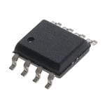
| 供应商器件封装 | 8-SOIC |
| 其它名称 | 296-3418-5 |
| 内部开关 | 是 |
| 包装 | 管件 |
| 单位重量 | 72.600 mg |
| 商标 | Texas Instruments |
| 安装类型 | 表面贴装 |
| 安装风格 | SMD/SMT |
| 封装 | Tube |
| 封装/外壳 | 8-SOIC(0.154",3.90mm 宽) |
| 封装/箱体 | SOIC-8 |
| 工作温度 | 0°C ~ 85°C |
| 工作温度范围 | 0 C to + 85 C |
| 工厂包装数量 | 75 |
| 开关数量 | Single |
| 开关类型 | 通用 |
| 最大工作温度 | + 85 C |
| 最小工作温度 | 0 C |
| 标准包装 | 75 |
| 比率-输入:输出 | 1:1 |
| 特性 | - |
| 电压-负载 | 2.7 V ~ 5.5 V |
| 电压-输入 | 2.7 V ~ 5.5 V |
| 电流-输出(最大值) | 250mA |
| 电流限制 | 500mA |
| 电源电压-最大 | 5.5 V |
| 电源电压-最小 | 2.7 V |
| 类型 | 高端开关 |
| 系列 | TPS2055A |
| 输入类型 | 非反相 |
| 输出数 | 1 |
| 输出类型 | N 通道 |
| 配用 | /product-detail/zh/TPS2055AEVM-290/TPS2055AEVM-290-ND/1907596 |


- 商务部:美国ITC正式对集成电路等产品启动337调查
- 曝三星4nm工艺存在良率问题 高通将骁龙8 Gen1或转产台积电
- 太阳诱电将投资9.5亿元在常州建新厂生产MLCC 预计2023年完工
- 英特尔发布欧洲新工厂建设计划 深化IDM 2.0 战略
- 台积电先进制程称霸业界 有大客户加持明年业绩稳了
- 达到5530亿美元!SIA预计今年全球半导体销售额将创下新高
- 英特尔拟将自动驾驶子公司Mobileye上市 估值或超500亿美元
- 三星加码芯片和SET,合并消费电子和移动部门,撤换高东真等 CEO
- 三星电子宣布重大人事变动 还合并消费电子和移动部门
- 海关总署:前11个月进口集成电路产品价值2.52万亿元 增长14.8%


PDF Datasheet 数据手册内容提取
TPS2045A,, TPS2046A TPS2047A, TPS2048A, TPS2055A TPS2056A, TPS2057A, TPS2058A www.ti.com SLVS251C–SEPTEMBER2000–REVISEDJANUARY2008 CURRENT-LIMITED POWER-DISTRIBUTION SWITCHES FEATURES 1• 80-mΩHigh-SideMOSFETSwitch TPS2D0 4P5AAC, KTAPSG2E055A TPS2D0 4P6AAC, KTAPSG2E056A • 250mAContinuousCurrentPerChannel (TOP VIEW) (TOP VIEW) • IndependentThermalandShort-Circuit GND 1 8 OUT GND 1 8 OC1 ProtectionWithOvercurrentLogicOutput IN 2 7 OUT IN 2 7 OUT1 • OperatingRange:2.7-Vto5.5-V IN 3 6 OUT EN1† 3 6 OUT2 • CMOS-andTTL-CompatibleEnableInputs EN† 4 5 OC EN2† 4 5 OC2 • 2.5-msTypicalRiseTime • UndervoltageLockout TPS2047A, TPS2057A TPS2048A, TPS2058A • 10m AMaximumStandbySupplyCurrent D PACKAGE D PACKAGE (TOP VIEW) (TOP VIEW) forSingleandDual (20m AforTripleandQuad) GNDA 1 16 OC1 GNDA 1 16 OC1 • BidirectionalSwitch IN1 2 15 OUT1 IN1 2 15 OUT1 • AmbientTemperatureRange,0(cid:176) Cto85(cid:176) C EN1† 3 14 OUT2 EN1† 3 14 OUT2 EN2† 4 13 OC2 EN2† 4 13 OC2 • ESDProtection GNDB 5 12 OC3 GNDB 5 12 OC3 IN2 6 11 OUT3 IN2 6 11 OUT3 DESCRIPTION EN3† 7 10 NC EN3† 7 10 OUT4 The TPS2045A through TPS2048A and TPS2055A NC 8 9 NC EN4† 8 9 OC4 through TPS2058A power-distribution switches are intended for applications where heavy capacitive †All enable inputs are active high for the TPS205xA series. loadsandshortcircuitsarelikelytobeencountered. NC – No connect These devices incorporate 80-mΩ N-channel MOSFET high-side power switches for power-distribution systems that require multiple power switches in a single package. Each switch is controlled by an independent logic enable input. Gate drive is provided by an internal charge pump designed to control the power-switch rise times and fall times to minimize current surges during switching. The charge pump requires no external components andallowsoperationfromsuppliesaslowas2.7V. When the output load exceeds the current-limit threshold or a short is present, these devices limit the output current to a safe level by switching into a constant-current mode, pulling the overcurrent (OCx) logic output low. When continuous heavy overloads and short circuits increase the power dissipation in the switch, causing the junction temperature to rise, a thermal protection circuit shuts off the switch to prevent damage. Recovery from a thermal shutdown is automatic once the device has cooled sufficiently. Internal circuitry ensures the switch remains off until valid input voltage is present. These power-distribution switches are designed to current limit at 0.5A. 1 Pleasebeawarethatanimportantnoticeconcerningavailability,standardwarranty,anduseincriticalapplicationsof TexasInstrumentssemiconductorproductsanddisclaimerstheretoappearsattheendofthisdatasheet. PRODUCTIONDATAinformationiscurrentasofpublicationdate. Copyright©2000–2008,TexasInstrumentsIncorporated Products conform to specifications per the terms of the Texas Instruments standard warranty. Production processing does not necessarilyincludetestingofallparameters.
TPS2045A,, TPS2046A TPS2047A, TPS2048A, TPS2055A TPS2056A, TPS2057A, TPS2058A www.ti.com SLVS251C–SEPTEMBER2000–REVISEDJANUARY2008 Thesedeviceshavelimitedbuilt-inESDprotection.Theleadsshouldbeshortedtogetherorthedeviceplacedinconductivefoam duringstorageorhandlingtopreventelectrostaticdamagetotheMOSgates. AVAILABLEOPTIONS(1) RECOMMENDED PACKAGEDDEVICES TYPICALSHORT-CIRCUIT T ENABLE MAXIMUMCONTINUOUS CURRENTLIMITAT25(cid:176) C NUMBEROF A LOADCURRENT (A) SWITCHES SOIC(D)(2) (A) Activelow TPS2045AD Single Activehigh TPS2055AD Activelow TPS2046AD Dual Activehigh TPS2056AD 0(cid:176) Cto85(cid:176) C 0.25 0.5 Activelow TPS2047AD Triple Activehigh TPS2057AD Activelow TPS2048AD Quad Activehigh TPS2058AD (1) Forthemostcurrentpackageandorderinginformation,seethePackageOptionAddendumattheendofthisdocument,orseetheTI websiteatwww.ti.com. (2) TheDpackageisavailabletapedandreeled.AddanRsuffixtodevicetype(e.g.,TPS2045ADR) 2 SubmitDocumentationFeedback Copyright©2000–2008,TexasInstrumentsIncorporated ProductFolderLink(s):TPS2045ATPS2046A TPS2047A TPS2048A TPS2055ATPS2056A TPS2057A TPS2058A
TPS2045A,, TPS2046A TPS2047A, TPS2048A, TPS2055A TPS2056A, TPS2057A, TPS2058A www.ti.com SLVS251C–SEPTEMBER2000–REVISEDJANUARY2008 FUNCTIONAL BLOCK DIAGRAMS TPS2045A Power Switch † IN CS OUT Charge Pump Current EN‡ Driver Limit OC UVLO Thermal GND Sense †Current sense ‡Active high for TPS205xA series TPS2046A OC1 GND Thermal Sense EN1‡ Current Driver Limit Charge Pump † CS OUT1 UVLO Power Switch † IN CS OUT2 Charge Pump Current Driver Limit OC2 EN2‡ Thermal Sense †Current sense ‡Active high for TPS205xA series Copyright©2000–2008,TexasInstrumentsIncorporated SubmitDocumentationFeedback 3 ProductFolderLink(s):TPS2045ATPS2046A TPS2047A TPS2048A TPS2055ATPS2056A TPS2057A TPS2058A
TPS2045A,, TPS2046A TPS2047A, TPS2048A, TPS2055A TPS2056A, TPS2057A, TPS2058A www.ti.com SLVS251C–SEPTEMBER2000–REVISEDJANUARY2008 TPS2047A OC1 GNDA Thermal Sense EN1‡ Current Driver Limit Charge Pump † CS OUT1 UVLO Power Switch † IN1 CS OUT2 Charge Pump Current Driver Limit OC2 EN2‡ Thermal Sense Power Switch † IN2 CS OUT3 Charge Pump Current EN3‡ Driver Limit OC3 UVLO Thermal GNDB Sense †Current sense ‡Active high for TPS205xA series 4 SubmitDocumentationFeedback Copyright©2000–2008,TexasInstrumentsIncorporated ProductFolderLink(s):TPS2045ATPS2046A TPS2047A TPS2048A TPS2055ATPS2056A TPS2057A TPS2058A
TPS2045A,, TPS2046A TPS2047A, TPS2048A, TPS2055A TPS2056A, TPS2057A, TPS2058A www.ti.com SLVS251C–SEPTEMBER2000–REVISEDJANUARY2008 TPS2048A OC1 GNDA Thermal Sense EN1‡ Current Driver Limit Charge Pump † CS OUT UVLO 1 Power Switch † IN1 CS OUT 2 Charge Pump Current Driver Limit OC2 EN2‡ Thermal Sense OC3 GNDB Thermal Sense EN3‡ Current Driver Limit Charge Pump † CS OUT3 UVLO Power Switch † IN2 CS OUT4 Charge Pump Current Driver Limit OC4 EN4‡ Thermal Sense †Current sense ‡Active high for TPS205xA series Copyright©2000–2008,TexasInstrumentsIncorporated SubmitDocumentationFeedback 5 ProductFolderLink(s):TPS2045ATPS2046A TPS2047A TPS2048A TPS2055ATPS2056A TPS2057A TPS2058A
TPS2045A,, TPS2046A TPS2047A, TPS2048A, TPS2055A TPS2056A, TPS2057A, TPS2058A www.ti.com SLVS251C–SEPTEMBER2000–REVISEDJANUARY2008 TerminalFunctions TPS2045AANDTPS2055A TERMINAL NO. I/O DESCRIPTION NAME TPS2045A TPS2055A EN 4 - I Enableinput.Logiclowturnsonpowerswitch. EN - 4 I Enableinput.Logichighturnsonpowerswitch. GND 1 1 I Ground IN 2,3 2,3 I Inputvoltage OC 5 5 O Overcurrent.Opendrainoutputactivelow OUT 6,7,8 6,7,8 O Power-switchoutput TPS2046AANDTPS2056A TERMINAL NO. I/O DESCRIPTION NAME TPS2046A TPS2056A EN1 3 - I Enableinput.Logiclowturnsonpowerswitch,IN-OUT1. EN2 4 - I Enableinput.Logiclowturnsonpowerswitch,IN-OUT2. EN1 - 3 I Enableinput.Logichighturnsonpowerswitch,IN-OUT1. EN2 - 4 I Enableinput.Logichighturnsonpowerswitch,IN-OUT2. GND 1 1 I Ground IN 2 2 I Inputvoltage OC1 8 8 O Overcurrent.Opendrainoutputactivelow,forpowerswitch,IN-OUT1 OC2 5 5 O Overcurrent.Opendrainoutputactivelow,forpowerswitch,IN-OUT2 OUT1 7 7 O Power-switchoutput OUT2 6 6 O Power-switchoutput 6 SubmitDocumentationFeedback Copyright©2000–2008,TexasInstrumentsIncorporated ProductFolderLink(s):TPS2045ATPS2046A TPS2047A TPS2048A TPS2055ATPS2056A TPS2057A TPS2058A
TPS2045A,, TPS2046A TPS2047A, TPS2048A, TPS2055A TPS2056A, TPS2057A, TPS2058A www.ti.com SLVS251C–SEPTEMBER2000–REVISEDJANUARY2008 TerminalFunctions(continued) TPS2047AANDTPS2057A TERMINAL NO. I/O DESCRIPTION NAME TPS2047A TPS2057A EN1 3 - I Enableinput,logiclowturnsonpowerswitch,IN1-OUT1. EN2 4 - I Enableinput,logiclowturnsonpowerswitch,IN1-OUT2. EN3 7 - I Enableinput,logiclowturnsonpowerswitch,IN2-OUT3. EN1 - 3 I Enableinput,logichighturnsonpowerswitch,IN1-OUT1. EN2 - 4 I Enableinput,logichighturnsonpowerswitch,IN1-OUT2. EN3 - 7 I Enableinput,logichighturnsonpowerswitch,IN2-OUT3. GNDA 1 1 GroundforIN1switchandcircuitry. GNDB 5 5 GroundforIN2switchandcircuitry. IN1 2 2 I Inputvoltage IN2 6 6 I Inputvoltage NC 8,9,10 8,9,10 Noconnection OC1 16 16 O Overcurrent,opendrainoutputactivelow,IN1-OUT1 OC2 13 13 O Overcurrent,opendrainoutputactivelow,IN1-OUT2 OC3 12 12 O Overcurrent,opendrainoutputactivelow,IN2-OUT3 OUT1 15 15 O Power-switchoutput,IN1-OUT1 OUT2 14 14 O Power-switchoutput,IN1-OUT2 OUT3 11 11 O Power-switchoutput,IN2-OUT3 TPS2048AANDTPS2058A TERMINAL NO. I/O DESCRIPTION NAME TPS2048A TPS2058A EN1 3 - I Enableinput.logiclowturnsonpowerswitch,IN1-OUT1. EN2 4 - I Enableinput.Logiclowturnsonpowerswitch,IN1-OUT2. EN3 7 - I Enableinput.Logiclowturnsonpowerswitch,IN2-OUT3. EN4 8 - I Enableinput.Logiclowturnsonpowerswitch,IN2-OUT4. EN1 - 3 I Enableinput.Logichighturnsonpowerswitch,IN1-OUT1. EN2 - 4 I Enableinput.Logichighturnsonpowerswitch,IN1-OUT2. EN3 - 7 I Enableinput.Logichighturnsonpowerswitch,IN2-OUT3. EN4 - 8 I Enableinput.Logichighturnsonpowerswitch,IN2-OUT4. GNDA 1 1 GroundforIN1switchandcircuitry. GNDB 5 5 GroundforIN2switchandcircuitry. IN1 2 2 I Inputvoltage IN2 6 6 I Inputvoltage OC1 16 16 O Overcurrent.Opendrainoutputactivelow,IN1-OUT1 OC2 13 13 O Overcurrent.Opendrainoutputactivelow,IN1-OUT2 OC3 12 12 O Overcurrent.Opendrainoutputactivelow,IN2-OUT3 OC4 9 9 O Overcurrent.Opendrainoutputactivelow,IN2-OUT4 OUT1 15 15 O Power-switchoutput,IN1-OUT1 OUT2 14 14 O Power-switchoutput,IN1-OUT2 OUT3 11 11 O Power-switchoutput,IN2-OUT3 OUT4 10 10 O Power-switchoutput,IN2-OUT4 Copyright©2000–2008,TexasInstrumentsIncorporated SubmitDocumentationFeedback 7 ProductFolderLink(s):TPS2045ATPS2046A TPS2047A TPS2048A TPS2055ATPS2056A TPS2057A TPS2058A
TPS2045A,, TPS2046A TPS2047A, TPS2048A, TPS2055A TPS2056A, TPS2057A, TPS2058A www.ti.com SLVS251C–SEPTEMBER2000–REVISEDJANUARY2008 DETAILED DESCRIPTION POWER SWITCH The power switch is an N-channel MOSFET with a maximum on-state resistance of 135 mΩ (V = 5 V). I(IN) Configured as a high-side switch, the power switch prevents current flow from OUT to IN and IN to OUT when disabled.Thepowerswitchsuppliesaminimumof250mAperswitch. CHARGE PUMP An internal charge pump supplies power to the driver circuit and provides the necessary voltage to pull the gate of the MOSFET above the source. The charge pump operates from input voltages as low as 2.7 V and requires verylittlesupplycurrent. DRIVER The driver controls the gate voltage of the power switch. To limit large current surges and reduce the associated electromagnetic interference (EMI) produced, the driver incorporates circuitry that controls the rise times and fall timesoftheoutputvoltage.Theriseandfalltimesaretypicallyinthe2-msto4-msrange. ENABLE (ENx, ENx) Thelogicenabledisablesthepowerswitchandthebiasforthechargepump,driver,andothercircuitryto reduce the supply current. The supply current is reduced to less than 10 m A on the single and dual devices (20 m A on the triple and quad devices) when a logic high is present on ENx (TPS204xA 1) or a logic low is present on ENx (TPS205xA1). A logic zero input on ENx or a logic high on ENx restores bias to the drive and control circuits and turnsthepoweron.TheenableinputiscompatiblewithbothTTLandCMOSlogiclevels. OVERCURRENT (OCx) The OCx open-drain output is asserted (active low) when an overcurrent or over temperature condition is encountered.Theoutputwillremainasserteduntiltheovercurrentorovertemperatureconditionisremoved. CURRENT SENSE A sense FET monitors the current supplied to the load. The sense FET measures current more efficiently than conventional resistance methods. When an overload or short circuit is encountered, the current-sense circuitry sends a control signal to the driver. The driver in turn reduces the gate voltage and drives the power FET into its saturation region, which switches the output into a constant-current mode and holds the current constant while varyingthevoltageontheload. THERMAL SENSE The TPS204xA and TPS205xA implement a dual-threshold thermal trip to allow fully independent operation of the power distribution switches. In an overcurrent or short-circuit condition the junction temperature rises. When the die temperature rises to approximately 140(cid:176) C, the internal thermal sense circuitry checks to determine which power switch is in an overcurrent condition and turns off that switch, thus isolating the fault without interrupting operationoftheadjacentpowerswitch.Hysteresisisbuiltintothethermalsense,andafterthe device has cooled approximately 20 degrees, the switch turns back on. The switch continues to cycle off and on until the fault is removed.The(OCx)open-drainoutputisasserted(activelow)whenovertemperatureorovercurrentoccurs. UNDERVOLTAGE LOCKOUT A voltage sense circuit monitors the input voltage. When the input voltage is below approximately 2 V, a control signalturnsoffthepowerswitch. 8 SubmitDocumentationFeedback Copyright©2000–2008,TexasInstrumentsIncorporated ProductFolderLink(s):TPS2045ATPS2046A TPS2047A TPS2048A TPS2055ATPS2056A TPS2057A TPS2058A
TPS2045A,, TPS2046A TPS2047A, TPS2048A, TPS2055A TPS2056A, TPS2057A, TPS2058A www.ti.com SLVS251C–SEPTEMBER2000–REVISEDJANUARY2008 ABSOLUTE MAXIMUM RATINGS overoperatingfree-airtemperaturerange(unlessotherwisenoted)(1) UNIT V Inputvoltagerange(2) 0.3Vto6V I(IN) V Outputvoltagerange(2) –0.3VtoV +0.3V O(OUT) I(IN) V orV Inputvoltagerange –0.3Vto6V I(ENx) I(ENx) I Continuousoutputcurrent internallylimited O(OUT) Continuoustotalpowerdissipation SeeDissipationRatingTable T Operatingvirtualjunctiontemperaturerange 0(cid:176) Cto125(cid:176) C J T Storagetemperaturerange –65(cid:176) Cto150(cid:176) C stg Leadtemperaturesoldering1,6mm(1/16inch)fromcasefor10seconds 260(cid:176) C HumanbodymodelMIL-STD-883C 2kV ESD Electrostaticdischargeprotection Machinemodel 0.2kV (1) Stressesbeyondthoselistedunder"absolutemaximumratings"maycausepermanentdamagetothedevice.Thesearestressratings only,andfunctionaloperationofthedeviceattheseoranyotherconditionsbeyondthoseindicatedunder"recommendedoperating conditions"isnotimplied.Exposuretoabsolute-maximum-ratedconditionsforextendedperiodsmayaffectdevicereliability. (2) AllvoltagesarewithrespecttoGND. DISSIPATION RATING TABLE T ≤25(cid:176) C DERATINGFACTOR T =70(cid:176) C T =85(cid:176) C PACKAGE POWAERRATING ABOVET =25(cid:176) C POWAERRATING POWAERRATING A D-8 725mW 5.9mW/(cid:176) C 464mW 377mW D-16 1123mW 9mW/(cid:176) C 719mW 584mW RECOMMENDED OPERATING CONDITIONS MIN MAX UNIT V Inputvoltage 2.7 5.5 V I(IN) V orV Inputvoltage 0 5.5 V I(EN) I(EN) I Continuousoutputcurrent(perswitch) 0 250 mA O(OUT) T Operatingvirtualjunctiontemperature 0 125 (cid:176) C J Copyright©2000–2008,TexasInstrumentsIncorporated SubmitDocumentationFeedback 9 ProductFolderLink(s):TPS2045ATPS2046A TPS2047A TPS2048A TPS2055ATPS2056A TPS2057A TPS2058A
TPS2045A,, TPS2046A TPS2047A, TPS2048A, TPS2055A TPS2056A, TPS2057A, TPS2058A www.ti.com SLVS251C–SEPTEMBER2000–REVISEDJANUARY2008 ELECTRICAL CHARACTERISTICS OVER RECOMMENDED OPERATING JUNCTION TEMPERATURE RANGE V =5.5V,I =ratedcurrent,V =V (unlessotherwisenoted) I(IN) O I(EN) I(IN) TPS204xA TPS205xA PARAMETER TESTCONDITIONS(1) UNIT MIN TYP MAX MIN TYP MAX V =5V, T =25(cid:176) C, I(IN) J 80 100 80 100 I =0.25A O Staticdrain-sourceon-stateresistance, V =5V, T =85(cid:176) C, I(IN) J 90 120 90 120 5-Voperation I =0.25A O V =5V, T =125(cid:176) C, I(IN) J 100 135 100 135 I =0.25A O r mΩ DS(on) V =3.3V, T =25(cid:176) C, I(IN) J 90 125 90 125 I =0.25A O Staticdrain-sourceon-stateresistance, V =3.3V, T =85(cid:176) C, I(IN) J 110 145 110 145 3.3-Voperation I =0.25A O V =3.3V, T =125(cid:176) C, I(IN) J 120 160 120 160 I =0.25A O V =5.5V, T =25(cid:176) C, CI(IN=)1m F, RJ =20Ω 2.5 2.5 L L t Risetime,output ms r V =2.7V, T =25(cid:176) C, CI(IN=)1m F, RJ =20Ω 3 3 L L V =5.5V, T =25(cid:176) C, CI(IN=)1m F, RJ =20Ω 4.4 4.4 L L t Falltime,output ms f V =2.7V, T =25(cid:176) (cid:176) C, CI(IN=)1m F, RJ =20Ω 2.5 2.5 L L (1) Pulse-testingtechniquesmaintainjunctiontemperatureclosetoambienttemperature;thermaleffectsmustbetakenintoaccount separately. ENABLE INPUT ENx OR ENx TPS204xA TPS205xA PARAMETER TESTCONDITIONS UNIT MIN TYP MAX MIN TYP MAX V high-levelinputvoltage 2.7V≤V ≤5.5V 2 2 V IH I(IN) 4.5V≤V ≤5.5V 0.8 0.8 I(IN) V Low-levelinputvoltage V IL 2.7V≤V ≤4.5V 0.4 0.4 I(IN) TPS204xA V =0VorV =V –0.5 0.5 I Inputcurrent I(ENx) I(ENx) I(IN) m A I TPS205xA V =V orV =0V –0.5 0.5 I(ENx) I(IN) I(ENx) t Turnontime C =100m F,R =20Ω 20 20 on L L ms t Turnofftime C =100m F,R =20Ω 40 40 off L L CURRENT LIMIT TPS204xA TPS205xA PARAMETER TESTCONDITIONS(1) UNIT MIN TYP MAX MIN TYP MAX V =5V,OUTconnectedtoGND, I Short-circuitoutputcurrent I(IN) 0.3 0.5 0.7 0.3 0.5 0.7 A OS Deviceenabledintoshortcircuit (1) Pulse-testingtechniquesmaintainjunctiontemperatureclosetoambienttemperature;thermaleffectsmustbetakenintoaccount separately. 10 SubmitDocumentationFeedback Copyright©2000–2008,TexasInstrumentsIncorporated ProductFolderLink(s):TPS2045ATPS2046A TPS2047A TPS2048A TPS2055ATPS2056A TPS2057A TPS2058A
TPS2045A,, TPS2046A TPS2047A, TPS2048A, TPS2055A TPS2056A, TPS2057A, TPS2058A www.ti.com SLVS251C–SEPTEMBER2000–REVISEDJANUARY2008 SUPPLY CURRENT (TPS2045A, TPS2055A) TPS2045A TPS2055A PARAMETER TESTCONDITIONS UNIT MIN TYP MAX MIN TYP MAX T =25(cid:176) C 0.025 1 J V =V Supplycurrent, NoLoad I(EN) I(IN) 40(cid:176) C≤TJ≤125(cid:176) C 10 m A low-leveloutput onOUT T =25(cid:176) C 0.025 1 J V =0V I(EN) 40(cid:176) C≤T ≤125(cid:176) C 10 J T =25(cid:176) C 85 110 J V =0V Supplycurrent, NoLoad I(EN) 40(cid:176) C≤TJ≤125(cid:176) C 100 m A high-leveloutput onOUT T =25(cid:176) C 85 110 J V =V I(EN) I(IN) 40(cid:176) C≤T ≤125(cid:176) C 100 J OUT V =V 40(cid:176) C≤T ≤125(cid:176) C 100 I(EN) I(IN) J Leakagecurrent connected m A toground VI(EN)=0V 40(cid:176) C≤TJ≤125(cid:176) C 100 Reverseleakage IN=High VI(EN)=0V T =25(cid:176) C 0.3 m A current impedance V =V J 0.3 I(EN) I(IN) SUPPLY CURRENT (TPS2046A, TPS2056A) TPS2046A TPS2056A PARAMETER TESTCONDITIONS UNIT MIN TYP MAX MIN TYP MAX T =25(cid:176) C 0.025 1 J V =V Supplycurrent, NoLoad I(ENx) I(IN) 40(cid:176) C≤TJ≤125(cid:176) C 10 m A low-leveloutput onOUT T =25(cid:176) C 0.025 1 J V =0V I(ENx) 40(cid:176) C≤T ≤125(cid:176) C 10 J T =25(cid:176) C 85 110 J V =0V Supplycurrent, NoLoad I(ENx) 40(cid:176) C≤TJ≤125(cid:176) C 100 m A high-leveloutput onOUT T =25(cid:176) C 85 110 J V =V I(ENx) I(IN) 40(cid:176) C≤T ≤125(cid:176) C 100 J OUT V =V 40(cid:176) C≤T ≤125(cid:176) C 100 I(ENx) I(IN) J Leakagecurrent connected m A toground VI(ENx)=0V 40(cid:176) C≤TJ≤125(cid:176) C 100 Reverseleakage IN=high VI(EN)=0V T =25(cid:176) C 0.3 m A current impedance V =V J 0.3 I(EN) I(IN) Copyright©2000–2008,TexasInstrumentsIncorporated SubmitDocumentationFeedback 11 ProductFolderLink(s):TPS2045ATPS2046A TPS2047A TPS2048A TPS2055ATPS2056A TPS2057A TPS2058A
TPS2045A,, TPS2046A TPS2047A, TPS2048A, TPS2055A TPS2056A, TPS2057A, TPS2058A www.ti.com SLVS251C–SEPTEMBER2000–REVISEDJANUARY2008 SUPPLY CURRENT (TPS2047A, TPS2057A) TPS2047A TPS2057A PARAMETER TESTCONDITIONS UNIT MIN TYP MAX MIN TYP MAX T =25(cid:176) C 0.05 2 J V =V Supplycurrent, Noloadon I(ENx) I(INx) 40(cid:176) C≤TJ≤125(cid:176) C 20 m A low-leveloutput OUTx T =25(cid:176) C 0.05 2 J V =0V I(ENx) 40(cid:176) C≤T ≤125(cid:176) C 20 J T =25(cid:176) C 160 200 J V =0V Supplycurrent, Noloadon I(ENx) 40(cid:176) C≤TJ≤125(cid:176) C 200 m A high-leveloutput OUTx T =25(cid:176) C 160 200 J V =V I(ENx) I(INx) 40(cid:176) C≤T ≤125(cid:176) C 200 J OUTx V =V 40(cid:176) C≤T ≤125(cid:176) C 200 I(ENx) I(INx) J Leakagecurrent connected m A toground VI(ENx)=0V 40(cid:176) C≤TJ≤125(cid:176) C 200 Reverseleakage IN=high VI(ENx)=0V T =25(cid:176) C 0.3 m A current impedance V =V J 0.3 I(ENx) I(IN) SUPPLY CURRENT (TPS2048A, TPS2058A) TPS2048A TPS2058A PARAMETER TESTCONDITIONS UNIT MIN TYP MAX MIN TYP MAX T =25(cid:176) C 0.05 2 J V =V Supplycurrent, NoLoadon I(ENx) I(INx) 40(cid:176) C≤TJ≤125(cid:176) C 20 m A low-leveloutput OUTx T =25(cid:176) C 0.05 2 J V =0V I(ENx) 40(cid:176) C≤T ≤125(cid:176) C 20 J T =25(cid:176) C 170 220 J V =0V Supplycurrent, NoLoadon I(ENx) 40(cid:176) C≤TJ≤125(cid:176) C 200 m A high-leveloutput OUTx T =25(cid:176) C 170 220 J V =V I(ENx) I(INx) 40(cid:176) C≤T ≤125(cid:176) C 200 J OUTx V =V 40(cid:176) C≤T ≤125(cid:176) C 200 I(ENx) I(INx) J Leakagecurrent connected m A toground VI(ENx)=0V 40(cid:176) C≤TJ≤125(cid:176) C 200 Reverseleakage IN=high VI(EN)=0V T =25(cid:176) C 0.3 m A current impedance V =V J 0.3 I(EN) I(IN) UNDERVOLTAGE LOCKOUT TPS204xA TPS205xA PARAMETER TESTCONDITIONS UNIT MIN TYP MAX MIN TYP MAX Low-levelinputvoltage 2 2.5 2 2.5 V Hysteresis T =25(cid:176) C 100 100 mV J OVERCURRENT OC TPS204xA TPS205xA PARAMETER TESTCONDITIONS UNIT MIN TYP MAX MIN TYP MAX Sinkcurrent(1) V =5V 10 10 mA O Outputlowvoltage I =5V,V 0.5 0.5 V O OL(OC) Off-statecurrent(1) V =5V,V =3.3V 1 1 m A O O (1) Specifiedbydesign,notproductiontested. 12 SubmitDocumentationFeedback Copyright©2000–2008,TexasInstrumentsIncorporated ProductFolderLink(s):TPS2045ATPS2046A TPS2047A TPS2048A TPS2055ATPS2056A TPS2057A TPS2058A
TPS2045A,, TPS2046A TPS2047A, TPS2048A, TPS2055A TPS2056A, TPS2057A, TPS2058A www.ti.com SLVS251C–SEPTEMBER2000–REVISEDJANUARY2008 PARAMETER MEASUREMENT INFORMATION OUT tr tf RL CL VO(OUT) 90% 90% 10% 10% TEST CIRCUIT VI(EN) 50% 50% VI(EN) 50% 50% ton toff ton toff VO(OUT) 90% VO(OUT) 90% 10% 10% VOLTAGE WAVEFORMS Figure1.TestCircuitandVoltageWaveforms VI(EN) VI(EN) (5 V/div) (5 V/div) VI(IN) = 5 V VI(IN) = 5 V TA = 25°C TA = 25°C VO(OUT) CL = 0.1 m F VO(OUT) CL = 0.1 m F (2 V/div) RL = 20 W (2 V/div) RL = 20 W 0 1 2 3 4 5 6 7 8 9 10 0 2 4 6 8 10 12 14 16 18 20 t − Time − ms t − Time − ms Figure2.TurnonDelayandRiseTime Figure3.TurnoffDelayandRiseTime With0.1-m FLoad With0.1-m FLoad Copyright©2000–2008,TexasInstrumentsIncorporated SubmitDocumentationFeedback 13 ProductFolderLink(s):TPS2045ATPS2046A TPS2047A TPS2048A TPS2055ATPS2056A TPS2057A TPS2058A
TPS2045A,, TPS2046A TPS2047A, TPS2048A, TPS2055A TPS2056A, TPS2057A, TPS2058A www.ti.com SLVS251C–SEPTEMBER2000–REVISEDJANUARY2008 PARAMETER MEASUREMENT INFORMATION (continued) VI(EN) VI(EN) (5 V/div) (5 V/div) (V2 OV(/OdUivT)) VTCRAILL( I =N== ) 2 21=50 m°5 WCF V V(2O (VO/dUiTv)) VTCRAILL( I =N== ) 2 21=50 m°5 WCF V 0 1 2 3 4 5 6 7 8 9 10 0 2 4 6 8 10 12 14 16 18 20 t − Time − ms t − Time − ms Figure4.TurnonDelayandRiseTime Figure5.TurnoffDelayandFallTime With1-m FLoad With1-m FLoad VI(IN) = 5 V TA = 25°C VI(ENx) RAMP: 1A/10ms (5 V/div) VO(OUT) (2 V/div) VI(IN) = 5 V IO(OUTx) TA = 25°C IO(OUT) (0.2 A/div) (0.2 A/div) 0 1 2 3 4 5 6 7 8 9 10 0 10 20 30 40 50 60 70 80 90 100 t − Time − ms t − Time − ms Figure6.TPS2055A,Short-CircuitCurrent, Figure7.TPS2055A,ThresholdTripCurrent DeviceEnabledIntoShort WithRampedLoadonEnabledDevice 14 SubmitDocumentationFeedback Copyright©2000–2008,TexasInstrumentsIncorporated ProductFolderLink(s):TPS2045ATPS2046A TPS2047A TPS2048A TPS2055ATPS2056A TPS2057A TPS2058A
TPS2045A,, TPS2046A TPS2047A, TPS2048A, TPS2055A TPS2056A, TPS2057A, TPS2058A www.ti.com SLVS251C–SEPTEMBER2000–REVISEDJANUARY2008 PARAMETER MEASUREMENT INFORMATION (continued) VI(IN) = 5 V TA = 25°C RAMP: 1A/100 ms VO(OC) VI(EN) (5 V/div) (5 V/div) 220 m F 100 m F 47 m F VI(IN) = 5 V IO(OUT) IO(OUT) TA = 25°C (0.2 A/div) (0.2 A/div) RL = 20 W 0 20 40 60 80 100 120 140 160 180 200 0 2 4 6 8 10 12 14 16 18 20 t − Time − ms t − Time − ms Figure8.OCResponseWithRampedLoad Figure9.InrushCurrentWith47-m F,100-m F onEnabledDevice and220-m FLoadCapacitance VI(IN) = 5 V VI(IN) = 5 V TA = 25°C TA = 25°C VO(OC) VO(OC) (5 V/div) (5 V/div) IO(OUT) IO(OUT) (0.5 A/div) (1 A/div) 0 200 400 600 800 1000 0 200 400 600 800 1000 t − Time − m s t − Time − m s Figure10.4-ΩLoadConnectedto Figure11.1-ΩLoadConnectedto EnabledDevice EnabledDevice Copyright©2000–2008,TexasInstrumentsIncorporated SubmitDocumentationFeedback 15 ProductFolderLink(s):TPS2045ATPS2046A TPS2047A TPS2048A TPS2055ATPS2056A TPS2057A TPS2058A
TPS2045A,, TPS2046A TPS2047A, TPS2048A, TPS2055A TPS2056A, TPS2057A, TPS2058A www.ti.com SLVS251C–SEPTEMBER2000–REVISEDJANUARY2008 TYPICAL CHARACTERISTICS TURNONDELAYTIME TURNOFFDELAYTIME vs vs INPUTVOLTAGE INPUTVOLTAGE 3.9 10 CL = 1 m F CL = 1 m F RL = 20 W RL = 20 W 3.6 TA = 25°C TA = 25°C 8 s s m m − − e e m 3.3 m Ti Ti ay ay 6 el el D D n 3 n o o n n ur ur T T 4 2.7 2.4 2 2.5 3 3.5 4 4.5 5 5.5 6 2.5 3 3.5 4 4.5 5 5.5 6 VI − Input Voltage − V VI − Input Voltage − V Figure12. Figure13. RISETIME FALLTIME vs vs INPUTVOLTAGE INPUTVOLTAGE 2.7 1.9 CL = 1 m F CL = 1 m F RL = 20 W RL = 20 W 2.6 TA = 25°C 1.8 TA = 25°C 2.5 ms ms 1.7 − − e 2.4 e m m Ti Ti 1.6 Rise 2.3 Fall − − t t 1.5 r f 2.2 1.4 2.1 2 1.3 2.5 3 3.5 4 4.5 5 5.5 6 2.5 3 3.5 4 4.5 5 5.5 6 VI − Input Voltage − V VI − Input Voltage − V Figure14. Figure15. 16 SubmitDocumentationFeedback Copyright©2000–2008,TexasInstrumentsIncorporated ProductFolderLink(s):TPS2045ATPS2046A TPS2047A TPS2048A TPS2055ATPS2056A TPS2057A TPS2058A
TPS2045A,, TPS2046A TPS2047A, TPS2048A, TPS2055A TPS2056A, TPS2057A, TPS2058A www.ti.com SLVS251C–SEPTEMBER2000–REVISEDJANUARY2008 TYPICAL CHARACTERISTICS (continued) SUPPLYCURRENT,OUTPUTENABLED SUPPLYCURRENT,OUTPUTDISABLED vs vs JUNCTIONTEMPERATURE JUNCTIONTEMPERATURE 100 160 A A n md − 90 ed − 140 VI(IN) = 5.5 V ble VI(IN) = 5.5 V abl 120 na VI(IN) = 5 V Dis nt, Output E 7800 VI(IN) = 4.5 V ent, Output 18000 VI(IN) V=I (4IN.5) =V 5 V urre VI(IN) = 2.7 V Curr 60 VI(IN) = 3.3 V ply C 60 pply VI(IN) = 2.7 V p u 40 u S − S 50 VI(IN) = 3.3 V − N) N) 20 II(I II(I 40 0 −40 0 25 85 125 −40 0 25 85 125 TJ − Junction Temperature − °C TJ − Junction Temperature − °C Figure16. Figure17. STATICDRAIN-SOURCEON-STATERESISTANCE INPUT-TO-OUTPUTVOLTAGE vs vs JUNCTIONTEMPERATURE LOADCURRENT 160 70 Wnce − m 140 VI(IN) = 2.7 V VI(IN) = 3.3 V ge − mV 60 TA = 25°C VI(IN) = 2.7 V a a sist 120 Volt 50 VI(IN) = 4.5 V ate Re 100 VI(IN) = 3 V utput VI(IN) = 3.3 V ource On-St 6800 VI(IN) = 5 V VI(IN) = 4.5 V − Input-to-O 3400 VI(IN) = 5 V n-S UT) 20 Drai 40 O(O c V Stati 20 −N) 10 − n) 0 VI(I 0 S(o 0 25 85 125 100 200 300 400 500 rD TJ − Junction Temperature − °C IL − Load Current − A Figure18. Figure19. Copyright©2000–2008,TexasInstrumentsIncorporated SubmitDocumentationFeedback 17 ProductFolderLink(s):TPS2045ATPS2046A TPS2047A TPS2048A TPS2055ATPS2056A TPS2057A TPS2058A
TPS2045A,, TPS2046A TPS2047A, TPS2048A, TPS2055A TPS2056A, TPS2057A, TPS2058A www.ti.com SLVS251C–SEPTEMBER2000–REVISEDJANUARY2008 TYPICAL CHARACTERISTICS (continued) SHORT-CIRCUITOUTPUTCURRENT THRESHOLDTRIPCURRENT vs vs JUNCTIONTEMPERATURE INPUTVOLTAGE 500 0.67 ent − mA 448900 VI(IN) = 3.3 V VI(IN) = 2.7 V A 0.65 TLAo a=d 2 R5°aCmp = 1 A/10 ms Curr 470 nt − ut 460 rre 0.63 cuit Outp 450 VI(IN) V= I(5INV) = 5 .5V VI(IN) = 4 .5V d Trip Cu Cir 440 hol 0.61 ort- 430 res h h S T − 420 0.59 S O I 410 0.57 400 −40 0 25 85 125 2.5 3 3.5 4 4.5 5 5.5 6 TJ − Junction Temperature − °C VI − Input Voltage − V Figure20. Figure21. UNDERVOLTAGELOCKOUT CURRENT-LIMITRESPONSE vs vs JUNCTIONTEMPERATURE PEAKCURRENT 2.36 300 2.34 Start Threshold 250 − V 2.32 ut s o 2.3 m− e Lock 2.28 ponse 200 g s a e rvolt 2.26 mit R 150 de 2.24 Li Un Stop Threshold nt- 100 O − 2.22 urre L C V 2.2 U 50 2.18 2.16 0 −40 0 25 85 125 0 2 4 6 8 10 TJ − Junction Temperature − °C Peak Current − A Figure22. Figure23. 18 SubmitDocumentationFeedback Copyright©2000–2008,TexasInstrumentsIncorporated ProductFolderLink(s):TPS2045ATPS2046A TPS2047A TPS2048A TPS2055ATPS2056A TPS2057A TPS2058A
TPS2045A,, TPS2046A TPS2047A, TPS2048A, TPS2055A TPS2056A, TPS2057A, TPS2058A www.ti.com SLVS251C–SEPTEMBER2000–REVISEDJANUARY2008 APPLICATION INFORMATION TPS2045A Power Supply 2,3 IN 2.7 V to 5.5 V 0.1 m F OUT 6,7,8 Load 0.1 m F 22 m F 5 OC 4 EN GND 1 Figure24.TypicalApplication(Example,TPS2045A) POWER-SUPPLY CONSIDERATIONS A 0.01-m F to 0.1-m F ceramic bypass capacitor between INx and GND, close to the device, is recommended. Placing a high-value electrolytic capacitor on the output pin(s) is recommended when the output load is heavy. This precaution reduces power-supply transients that may cause ringing on the input. Additionally, bypassing the outputwitha0.01-m Fto0.1-m Fceramiccapacitorimprovestheimmunityofthedevicetoshort-circuittransients. OVERCURRENT A sense FET is employed to check for overcurrent conditions. Unlike current-sense resistors, sense FETs do not increase the series resistance of the current path. When an overcurrent condition is detected, the device maintains a constant output current and reduces the output voltage accordingly. Complete shutdown occurs only ifthefaultispresentlongenoughtoactivatethermallimiting. Three possible overload conditions can occur. In the first condition, the output has been shorted before the device is enabled or before V has been applied (see Figure 6). The TPS204xA and TPS205xA sense the I(IN) shortandimmediatelyswitchintoaconstant-currentoutput. In the second condition, a short or an overload occurs while the device is enabled. At the instant the overload occurs, very high currents may flow for a short time before the current-limit circuit can react. After the current-limit circuit has tripped (reached the overcurrent trip threshold) the device switches into constant-current mode. In the third condition, the load has been gradually increased beyond the recommended operating current. The current is permitted to rise until the current-limit threshold is reached or until the thermal limit of the device is exceeded (see Figure 7). The TPS204xA and TPS205xA are capable of delivering current up to the current-limit threshold without damaging the device. Once the threshold has been reached, the device switches into its constant-currentmode. OC RESPONSE The OC open-drain output is asserted (active low) when an overcurrent or over temperature condition is encountered. The output will remain asserted until the overcurrent or over temperature condition is removed. Connecting a heavy capacitive load to an enabled device can cause momentary false overcurrent reporting from the inrush current flowing through the device, charging the downstream capacitor. The TPS204xA and TPS205xA family of devices are designed to reduce false overcurrent reporting. An internal overcurrent transient filter eliminates the need for external components to remove unwanted pulses. Using low-ESR electrolytic capacitors on the output lowers the inrush current flow through the device during hot-plug events by providing a low-impedanceenergysource,alsoreducingerroneousovercurrentreporting. Copyright©2000–2008,TexasInstrumentsIncorporated SubmitDocumentationFeedback 19 ProductFolderLink(s):TPS2045ATPS2046A TPS2047A TPS2048A TPS2055ATPS2056A TPS2057A TPS2058A
TPS2045A,, TPS2046A TPS2047A, TPS2048A, TPS2055A TPS2056A, TPS2057A, TPS2058A www.ti.com SLVS251C–SEPTEMBER2000–REVISEDJANUARY2008 TPS2045A GND OUT V+ IN OUT Rpullup IN OUT EN OC Figure25.TypicalCircuitforOCPin(Example,TPS2045A) POWER DISSIPATION AND JUNCTION TEMPERATURE The low on-resistance on the n-channel MOSFET allows small surface-mount packages, such as SOIC, to pass large currents. The thermal resistance of these packages is high compared to those of power packages; it is good design practice to check power dissipation and junction temperature. Begin by determining the r of the DS(on) N-channel MOSFET relative to the input voltage and operating temperature. As an initial estimate, use the highest operating ambient temperature of interest and read r from Figure 18. Using this value, the power DS(on) dissipationperswitchcanbecalculatedby: P (cid:2)r (cid:1)I2 D DS(on) Depending on which device is being used, multiply this number by the number of switches being used. This step willrenderthetotalpowerdissipationfromtheN-channelMOSFETs. Finally,calculatethejunctiontemperature: T (cid:3)P (cid:1)R (cid:2)T J D (cid:1)JA A Where: T = Ambient temperature (cid:176) C R = Thermal resistance SOIC = 172(cid:176) C/W (for 8 pin), 111(cid:176) C/W (for 16 A ΘJA pin)P =Totalpowerdissipationbasedonnumberofswitchesbeingused. D Compare the calculated junction temperature with the initial estimate. If they do not agree within a few degrees, repeat the calculation, using the calculated value as the new estimate. Two or three iterations are generally sufficienttogetareasonableanswer. THERMAL PROTECTION Thermal protection prevents damage to the IC when heavy-overload or short-circuit faults are present for extended periods of time. The faults force the TPS204xA and TPS205xA into constant-current mode, which causes the voltage across the high-side switch to increase; under short-circuit conditions, the voltage across the switch is equal to the input voltage. The increased dissipation causes the junction temperature to rise to high levels. The protection circuit senses the junction temperature of the switch and shuts it off. Hysteresis is built into the thermal sense circuit, and after the device has cooled approximately 20 degrees, the switch turns back on. Theswitchcontinuestocycleinthismanneruntiltheloadfaultorinputpowerisremoved. The TPS204xA and TPS205xA implement a dual thermal trip to allow fully independent operation of the power distribution switches. In an overcurrent or short-circuit condition the junction temperature will rise. Once the die temperaturerisestoapproximately140(cid:176) C,theinternalthermalsensecircuitry checks which power switch is in an overcurrent condition and turns that power switch off, thus isolating the fault without interrupting operation of the adjacent power switch. Should the die temperature exceed the first thermal trip point of 140(cid:176) C and reach 160(cid:176) C, both switches turn off. The OC open-drain output is asserted (active low) when overtemperature or overcurrent occurs. UNDERVOLTAGE LOCKOUT (UVLO) An undervoltage lockout ensures that the power switch is in the off state at power up. Whenever the input voltage falls below approximately 2 V, the power switch will be quickly turned off. This facilitates the design of hot-insertion systems where it is not possible to turn off the power switch before input power is removed. The UVLO will also keep the switch from being turned on until the power supply has reached at least 2 V, even if the switch is enabled. Upon reinsertion, the power switch will be turned on, with a controlled rise time to reduce EMI andvoltageovershoots. 20 SubmitDocumentationFeedback Copyright©2000–2008,TexasInstrumentsIncorporated ProductFolderLink(s):TPS2045ATPS2046A TPS2047A TPS2048A TPS2055ATPS2056A TPS2057A TPS2058A
TPS2045A,, TPS2046A TPS2047A, TPS2048A, TPS2055A TPS2056A, TPS2057A, TPS2058A www.ti.com SLVS251C–SEPTEMBER2000–REVISEDJANUARY2008 UNIVERSAL SERIAL BUS (USB) APPLICATIONS The universal serial bus (USB) interface is a 12-Mb/s, or 1.5-Mb/s, multiplexed serial bus designed for low-to-medium bandwidth PC peripherals (e.g., keyboards, printers, scanners, and mice). The four-wire USB interface is conceived for dynamic attach-detach (hot plug-unplug) of peripherals. Two lines are provided for differentialdata,andtwolinesareprovidedfor5-Vpowerdistribution. USB data is a 3.3-V level signal, but power is distributed at 5 V to allow for voltage drops in cases where power is distributed through more than one hub across long cables. Each function must provide its own regulated 3.3V fromthe5-Vinputoritsowninternalpowersupply. The USB specification defines the following five classes of devices, each differentiated by power-consumption requirements: • Hosts/self-poweredhubs(SPH) • Bus-poweredhubs(BPH) • Low-power,bus-poweredfunctions • High-power,bus-poweredfunctions • Self-poweredfunctions Self-powered and bus-powered hubs distribute data and power to downstream functions. The TPS204xA and TPS205xAcanprovidepower-distributionsolutionsformanyoftheseclassesofdevices. HOST/SELF-POWERED AND BUS-POWERED HUBS Hosts and self-powered hubs have a local power supply that powers the embedded functions and the downstream ports. This power supply must provide from 5.25 V to 4.75 V to the board side of the downstream connection under full-load and no-load conditions. Hosts and SPHs are required to have current-limit protection and must report overcurrent conditions to the USB controller. Typical SPHs are desktop PCs, monitors, printers, andstand-alonehubs. Bus-powered hubs obtain all power from upstream ports and often contain an embedded function. The hubs are required to power up with less than one unit load. The BPH usually has one embedded function, and power is always available to the controller of the hub. If the embedded function and hub require more than 100 mA on power up, the power to the embedded function may need to be kept off until enumeration is completed. This can be accomplished by removing power or by shutting off the clock to the embedded function. Power switching the embedded function is not necessary if the aggregate power draw for the function and controller is less than one unit load. The total current drawn by the bus-powered device is the sum of the current to the controller, the embeddedfunction,andthedownstreamports,anditislimitedto500mAfromanupstreamport. LOW-POWER BUS-POWERED FUNCTIONS AND HIGH-POWER BUS-POWERED FUNCTIONS Both low-power and high-power bus-powered functions obtain all power from upstream ports; low-power functions always draw less than 100 mA (see Figure 26); high-power functions must draw less than 100 mA at power up and can draw up to 500 mA after enumeration. If the load of the function is more than the parallel combinationof44Ωand10m Fatpowerup,thedevicemustimplementinrushcurrentlimiting. Power Supply D+ 3.3 V TPS2045A D– 2,3 VBUS 10 m F 0.1 m F IN 6, 7, 8 GND OUT Internal 0.1 m F 10 m F Function 5 USB OC Control 4 EN GND 1 Figure26.Low-PowerBus-PoweredFunction(Example,TPS2045A) Copyright©2000–2008,TexasInstrumentsIncorporated SubmitDocumentationFeedback 21 ProductFolderLink(s):TPS2045ATPS2046A TPS2047A TPS2048A TPS2055ATPS2056A TPS2057A TPS2058A
TPS2045A,, TPS2046A TPS2047A, TPS2048A, TPS2055A TPS2056A, TPS2057A, TPS2058A www.ti.com SLVS251C–SEPTEMBER2000–REVISEDJANUARY2008 USB POWER-DISTRIBUTION REQUIREMENTS USB can be implemented in several ways, and, regardless of the type of USB device being developed, several power-distributionfeaturesmustbeimplemented. • Hosts/self-poweredhubsmust: – Current-limitdownstreamports – ReportovercurrentconditionsonUSBV BUS – Enable/disablepowertodownstreamports – Powerupat<100mA – Limitinrushcurrent(<44Ωand10m F) – Limitinrushcurrents – Powerupat<100mA • Bus-poweredhubsmust: – Enable/disablepowertodownstreamports – Powerupat<100mA – Limitinrushcurrent(<44Ωand10m F) – Limitinrushcurrents – Powerupat<100mA • Functionsmust: – Limitinrushcurrents – Powerupat<100mA The feature set of the TPS204xA and TPS205xA allows them to meet each of these requirements. The integrated current-limiting and overcurrent reporting is required by hosts and self-powered hubs. The logic-level enable and controlled rise times meet the need of both input and output ports on bus-power hubs, as well as the inputportsforbus-powerfunctions. 22 SubmitDocumentationFeedback Copyright©2000–2008,TexasInstrumentsIncorporated ProductFolderLink(s):TPS2045ATPS2046A TPS2047A TPS2048A TPS2055ATPS2056A TPS2057A TPS2058A
TPS2045A,, TPS2046A TPS2047A, TPS2048A, TPS2055A TPS2056A, TPS2057A, TPS2058A www.ti.com SLVS251C–SEPTEMBER2000–REVISEDJANUARY2008 TUSB2040 Hub Controller SN75240 BUSPWR Upstream A C Downstream Port B D GANGE Ports D DP1 D + D + DP0 D − DM0 DM1 Ferrite Beads D − A C GND GND B D SN75240 DP2 5 V DM2 33 m F† DP3 5 V DM3 D + A C B D D − TPS76333 Ferrite Beads SN75240 GND IN DP4 0.1 m F DM4 4.7 m F 3.3 V 4.7 m F VCC TPS2045A 5 V GND GND PWRON1 EN IN 33 m F† OVRCUR1 OC 0.1 m F OUT D + TPS2045A D − 48-MHz XTAL1 PWRON2 EN IN Ferrite Beads Crystal OVRCUR2 OC 0.1 m F GND OUT Tuning 5 V XTAL2 TPS2045A Circuit PWRON3 EN IN 33 m F† OCSOFF OVRCUR3 OC 0.1 m F OUT D + GND TPS2045A D − Ferrite Beads PWRON4 EN IN GND OVRCUR4 OC 0.1 m F OUT 5 V 33 m F† †USB rev 1.1 requires 120 m F per hub. Figure27.Bus-PoweredHubImplementation,TPS2045A Copyright©2000–2008,TexasInstrumentsIncorporated SubmitDocumentationFeedback 23 ProductFolderLink(s):TPS2045ATPS2046A TPS2047A TPS2048A TPS2055ATPS2056A TPS2057A TPS2058A
TPS2045A,, TPS2046A TPS2047A, TPS2048A, TPS2055A TPS2056A, TPS2057A, TPS2058A www.ti.com SLVS251C–SEPTEMBER2000–REVISEDJANUARY2008 TUSB2040 Hub Controller SN75240 BUSPWR Upstream A C Downstream Port B D GANGE Ports D DP1 D + D + DP0 D − DM0 DM1 Ferrite Beads D − A C GND GND B D SN75240 DP2 5 V DM2 33 m F† DP3 5 V DM3 D + A C B D D − Ferrite Beads TPS76333 SN75240 GND IN DP4 0.1 m F DM4 4.7 m F 3.3 V 4.7 m F VCC TPS2046A 5 V GND GND PWRON1 EN1 OUT1 33 m F† OVRCUR1 OC1 OUT2 PWRON2 EN2 D + OVRCUR2 OC2 IN D − 48-MHz XTAL1 0.1 m F Ferrite Beads Crystal GND TPS2046A Tuning PWRON3 EN1 OUT1 5 V XTAL2 Circuit OVRCUR3 OC1 OUT2 33 m F† PWRON4 EN2 OCSOFF OVRCUR4 OC2 IN GND 0.1 m F D + D − Ferrite Beads GND 5 V 33 m F† †USB rev 1.1 requires 120 m F per hub. Figure28.Bus-PoweredHubImplementation,TPS2046A 24 SubmitDocumentationFeedback Copyright©2000–2008,TexasInstrumentsIncorporated ProductFolderLink(s):TPS2045ATPS2046A TPS2047A TPS2048A TPS2055ATPS2056A TPS2057A TPS2058A
TPS2045A,, TPS2046A TPS2047A, TPS2048A, TPS2055A TPS2056A, TPS2057A, TPS2058A www.ti.com SLVS251C–SEPTEMBER2000–REVISEDJANUARY2008 TUSB2040 Hub Controller 1/2 SN75240 BUSPWR Upstream A C Downstream Port B D GANGE Ports D DP1 D + D + DP0 D − DM0 DM1 Ferrite Beads D − A C GND GND B D SN75240 DP2 5 V DM2 47 m F† DP3 5 V DM3 D + A C B D D − Ferrite Beads TPS76333 1/2 SN75240 GND IN DP4 0.1 m F DM4 4.7 m F 3.3 V 4.7 m F VCC TPS2047A 5 V GND GND PWRON1 EN1 OUT1 47 m F† OVRCUR1 OC1 OUT2 PWRON2 EN2 D + OVRCUR2 OC2 IN1 D − 48-MHz XTAL1 0.1 m F Ferrite Beads Crystal GND Tuning PWRON3 EN3 OUT3 5 V XTAL2 Circuit OVRCUR3 OC3 47 m F† OCSOFF IN2 GND 0.1 m F GNDA GNDB †USB rev 1.1 requires 120 m F per hub. Figure29.Bus-PoweredHubImplementation,TPS2047A Copyright©2000–2008,TexasInstrumentsIncorporated SubmitDocumentationFeedback 25 ProductFolderLink(s):TPS2045ATPS2046A TPS2047A TPS2048A TPS2055ATPS2056A TPS2057A TPS2058A
TPS2045A,, TPS2046A TPS2047A, TPS2048A, TPS2055A TPS2056A, TPS2057A, TPS2058A www.ti.com SLVS251C–SEPTEMBER2000–REVISEDJANUARY2008 TUSB2040 Hub Controller SN75240 BUSPWR Upstream A C Downstream Port B D GANGE Ports D DP1 D + D + DP0 D − DM0 DM1 Ferrite Beads D − A C GND GND B D SN75240 DP2 5 V TPS2041A DM2 33 m F† DP3 5 V DM3 D + A C B D D − Ferrite Beads TPS76333 SN75240 GND IN DP4 0.1 m F DM4 4.7 m F 3.3 V 4.7 m F VCC TPS2048A 5 V GND GND PWRON1 EN1 OUT1 33 m F† OVRCUR1 OC1 OUT2 PWRON2 EN2 D + OVRCUR2 OC2 IN1 D − 48-MHz XTAL1 0.1 m F Ferrite Beads Crystal GND Tuning PWRON3 EN3 OUT3 5 V XTAL2 Circuit OVRCUR3 OC3 OUT4 33 m F† PWRON4 EN4 OCSOFF OVRCUR4 OC4 IN2 GND 0.1 m F D + D − Ferrite Beads GNDA GND GNDB 5 V 33 m F† †USB rev 1.1 requires 120 m F per hub. Figure30.Bus-PoweredHubImplementation,TPS2048A 26 SubmitDocumentationFeedback Copyright©2000–2008,TexasInstrumentsIncorporated ProductFolderLink(s):TPS2045ATPS2046A TPS2047A TPS2048A TPS2055ATPS2056A TPS2057A TPS2058A
TPS2045A,, TPS2046A TPS2047A, TPS2048A, TPS2055A TPS2056A, TPS2057A, TPS2058A www.ti.com SLVS251C–SEPTEMBER2000–REVISEDJANUARY2008 GENERIC HOT-PLUG APPLICATIONS (see Figure 31) In many applications it may be necessary to remove modules or pc boards while the main unit is still operating. These are considered hot-plug applications. Such implementations require the control of current surges seen by the main power supply and the card being inserted. The most effective way to control these surges is to limit and slowly ramp the current and voltage being applied to the card, similar to the way in which a power supply normally turns on. Due to the controlled rise times and fall times of the TPS204xA and TPS205xA, these devices can be used to provide a softer start-up to devices being hot-plugged into a powered system. The UVLO feature of the TPS204xA and TPS205xA also ensures the switch will be off after the card has been removed, and the switch will be off during the next insertion. The UVLO feature insures a soft start with a controlled rise time for everyinsertionofthecardormodule. PC Board TPS2045A Power Block of Supply GND OUT Circuitry 2.7 V to 5.5 V IN OUT 1000 m F 0.1 m F IN OUT Optimum EN OC Overcurrent Response Figure31.TypicalHot-PlugImplementation(Example,TPS2045A) By placing the TPS204xA and TPS205xA between the V input and the rest of the circuitry, the input power will CC reach these devices first after insertion. The typical rise time of the switch is approximately 2.5 ms, providing a slow voltage ramp at the output of the device. This implementation controls system surge currents and provides ahot-pluggingmechanismforanydevice. Copyright©2000–2008,TexasInstrumentsIncorporated SubmitDocumentationFeedback 27 ProductFolderLink(s):TPS2045ATPS2046A TPS2047A TPS2048A TPS2055ATPS2056A TPS2057A TPS2058A
PACKAGE OPTION ADDENDUM www.ti.com 6-Feb-2020 PACKAGING INFORMATION Orderable Device Status Package Type Package Pins Package Eco Plan Lead/Ball Finish MSL Peak Temp Op Temp (°C) Device Marking Samples (1) Drawing Qty (2) (6) (3) (4/5) TPS2045AD ACTIVE SOIC D 8 75 Green (RoHS NIPDAU Level-1-260C-UNLIM 0 to 85 2045A & no Sb/Br) TPS2045ADR ACTIVE SOIC D 8 2500 Green (RoHS NIPDAU Level-1-260C-UNLIM 0 to 85 2045A & no Sb/Br) TPS2045ADRG4 ACTIVE SOIC D 8 2500 Green (RoHS NIPDAU Level-1-260C-UNLIM 0 to 85 2045A & no Sb/Br) TPS2046AD ACTIVE SOIC D 8 75 Green (RoHS NIPDAU Level-1-260C-UNLIM 0 to 85 2046A & no Sb/Br) TPS2048AD ACTIVE SOIC D 16 40 Green (RoHS NIPDAU Level-1-260C-UNLIM 0 to 85 2048A & no Sb/Br) TPS2048ADR ACTIVE SOIC D 16 2500 Green (RoHS NIPDAU Level-1-260C-UNLIM 0 to 85 2048A & no Sb/Br) TPS2048ADRG4 ACTIVE SOIC D 16 2500 Green (RoHS NIPDAU Level-1-260C-UNLIM 0 to 85 2048A & no Sb/Br) TPS2055AD ACTIVE SOIC D 8 75 Green (RoHS NIPDAU Level-1-260C-UNLIM 0 to 85 2055A & no Sb/Br) TPS2055ADR ACTIVE SOIC D 8 2500 Green (RoHS NIPDAU Level-1-260C-UNLIM 0 to 85 2055A & no Sb/Br) TPS2055ADRG4 ACTIVE SOIC D 8 2500 Green (RoHS NIPDAU Level-1-260C-UNLIM 0 to 85 2055A & no Sb/Br) TPS2056AD ACTIVE SOIC D 8 75 Green (RoHS NIPDAU Level-1-260C-UNLIM 0 to 85 2056A & no Sb/Br) TPS2056ADG4 ACTIVE SOIC D 8 75 Green (RoHS NIPDAU Level-1-260C-UNLIM 0 to 85 2056A & no Sb/Br) TPS2056ADR ACTIVE SOIC D 8 2500 Green (RoHS NIPDAU Level-1-260C-UNLIM 0 to 85 2056A & no Sb/Br) TPS2056ADRG4 ACTIVE SOIC D 8 2500 Green (RoHS NIPDAU Level-1-260C-UNLIM 0 to 85 2056A & no Sb/Br) TPS2057AD ACTIVE SOIC D 16 40 Green (RoHS NIPDAU Level-1-260C-UNLIM 0 to 85 2057A & no Sb/Br) TPS2057ADG4 ACTIVE SOIC D 16 40 Green (RoHS NIPDAU Level-1-260C-UNLIM 0 to 85 2057A & no Sb/Br) TPS2057ADR ACTIVE SOIC D 16 2500 Green (RoHS NIPDAU Level-1-260C-UNLIM 0 to 85 2057A & no Sb/Br) Addendum-Page 1
PACKAGE OPTION ADDENDUM www.ti.com 6-Feb-2020 Orderable Device Status Package Type Package Pins Package Eco Plan Lead/Ball Finish MSL Peak Temp Op Temp (°C) Device Marking Samples (1) Drawing Qty (2) (6) (3) (4/5) TPS2058AD ACTIVE SOIC D 16 40 Green (RoHS NIPDAU Level-1-260C-UNLIM 0 to 85 2058A & no Sb/Br) (1) The marketing status values are defined as follows: ACTIVE: Product device recommended for new designs. LIFEBUY: TI has announced that the device will be discontinued, and a lifetime-buy period is in effect. NRND: Not recommended for new designs. Device is in production to support existing customers, but TI does not recommend using this part in a new design. PREVIEW: Device has been announced but is not in production. Samples may or may not be available. OBSOLETE: TI has discontinued the production of the device. (2) RoHS: TI defines "RoHS" to mean semiconductor products that are compliant with the current EU RoHS requirements for all 10 RoHS substances, including the requirement that RoHS substance do not exceed 0.1% by weight in homogeneous materials. Where designed to be soldered at high temperatures, "RoHS" products are suitable for use in specified lead-free processes. TI may reference these types of products as "Pb-Free". RoHS Exempt: TI defines "RoHS Exempt" to mean products that contain lead but are compliant with EU RoHS pursuant to a specific EU RoHS exemption. Green: TI defines "Green" to mean the content of Chlorine (Cl) and Bromine (Br) based flame retardants meet JS709B low halogen requirements of <=1000ppm threshold. Antimony trioxide based flame retardants must also meet the <=1000ppm threshold requirement. (3) MSL, Peak Temp. - The Moisture Sensitivity Level rating according to the JEDEC industry standard classifications, and peak solder temperature. (4) There may be additional marking, which relates to the logo, the lot trace code information, or the environmental category on the device. (5) Multiple Device Markings will be inside parentheses. Only one Device Marking contained in parentheses and separated by a "~" will appear on a device. If a line is indented then it is a continuation of the previous line and the two combined represent the entire Device Marking for that device. (6) Lead/Ball Finish - Orderable Devices may have multiple material finish options. Finish options are separated by a vertical ruled line. Lead/Ball Finish values may wrap to two lines if the finish value exceeds the maximum column width. Important Information and Disclaimer:The information provided on this page represents TI's knowledge and belief as of the date that it is provided. TI bases its knowledge and belief on information provided by third parties, and makes no representation or warranty as to the accuracy of such information. Efforts are underway to better integrate information from third parties. TI has taken and continues to take reasonable steps to provide representative and accurate information but may not have conducted destructive testing or chemical analysis on incoming materials and chemicals. TI and TI suppliers consider certain information to be proprietary, and thus CAS numbers and other limited information may not be available for release. In no event shall TI's liability arising out of such information exceed the total purchase price of the TI part(s) at issue in this document sold by TI to Customer on an annual basis. Addendum-Page 2
PACKAGE MATERIALS INFORMATION www.ti.com 10-Oct-2018 TAPE AND REEL INFORMATION *Alldimensionsarenominal Device Package Package Pins SPQ Reel Reel A0 B0 K0 P1 W Pin1 Type Drawing Diameter Width (mm) (mm) (mm) (mm) (mm) Quadrant (mm) W1(mm) TPS2045ADR SOIC D 8 2500 330.0 12.4 6.4 5.2 2.1 8.0 12.0 Q1 TPS2048ADR SOIC D 16 2500 330.0 16.4 6.5 10.3 2.1 8.0 16.0 Q1 TPS2055ADR SOIC D 8 2500 330.0 12.4 6.4 5.2 2.1 8.0 12.0 Q1 TPS2056ADR SOIC D 8 2500 330.0 12.4 6.4 5.2 2.1 8.0 12.0 Q1 TPS2057ADR SOIC D 16 2500 330.0 16.4 6.5 10.3 2.1 8.0 16.0 Q1 PackMaterials-Page1
PACKAGE MATERIALS INFORMATION www.ti.com 10-Oct-2018 *Alldimensionsarenominal Device PackageType PackageDrawing Pins SPQ Length(mm) Width(mm) Height(mm) TPS2045ADR SOIC D 8 2500 340.5 338.1 20.6 TPS2048ADR SOIC D 16 2500 333.2 345.9 28.6 TPS2055ADR SOIC D 8 2500 340.5 338.1 20.6 TPS2056ADR SOIC D 8 2500 340.5 338.1 20.6 TPS2057ADR SOIC D 16 2500 333.2 345.9 28.6 PackMaterials-Page2
None
None
PACKAGE OUTLINE D0008A SOIC - 1.75 mm max height SCALE 2.800 SMALL OUTLINE INTEGRATED CIRCUIT C SEATING PLANE .228-.244 TYP [5.80-6.19] .004 [0.1] C A PIN 1 ID AREA 6X .050 [1.27] 8 1 2X .189-.197 [4.81-5.00] .150 NOTE 3 [3.81] 4X (0 -15 ) 4 5 8X .012-.020 B .150-.157 [0.31-0.51] .069 MAX [3.81-3.98] .010 [0.25] C A B [1.75] NOTE 4 .005-.010 TYP [0.13-0.25] 4X (0 -15 ) SEE DETAIL A .010 [0.25] .004-.010 0 - 8 [0.11-0.25] .016-.050 [0.41-1.27] DETAIL A (.041) TYPICAL [1.04] 4214825/C 02/2019 NOTES: 1. Linear dimensions are in inches [millimeters]. Dimensions in parenthesis are for reference only. Controlling dimensions are in inches. Dimensioning and tolerancing per ASME Y14.5M. 2. This drawing is subject to change without notice. 3. This dimension does not include mold flash, protrusions, or gate burrs. Mold flash, protrusions, or gate burrs shall not exceed .006 [0.15] per side. 4. This dimension does not include interlead flash. 5. Reference JEDEC registration MS-012, variation AA. www.ti.com
EXAMPLE BOARD LAYOUT D0008A SOIC - 1.75 mm max height SMALL OUTLINE INTEGRATED CIRCUIT 8X (.061 ) [1.55] SYMM SEE DETAILS 1 8 8X (.024) [0.6] SYMM (R.002 ) TYP [0.05] 5 4 6X (.050 ) [1.27] (.213) [5.4] LAND PATTERN EXAMPLE EXPOSED METAL SHOWN SCALE:8X SOLDER MASK SOLDER MASK METAL OPENING OPENING METAL UNDER SOLDER MASK EXPOSED METAL EXPOSED METAL .0028 MAX .0028 MIN [0.07] [0.07] ALL AROUND ALL AROUND NON SOLDER MASK SOLDER MASK DEFINED DEFINED SOLDER MASK DETAILS 4214825/C 02/2019 NOTES: (continued) 6. Publication IPC-7351 may have alternate designs. 7. Solder mask tolerances between and around signal pads can vary based on board fabrication site. www.ti.com
EXAMPLE STENCIL DESIGN D0008A SOIC - 1.75 mm max height SMALL OUTLINE INTEGRATED CIRCUIT 8X (.061 ) [1.55] SYMM 1 8 8X (.024) [0.6] SYMM (R.002 ) TYP [0.05] 5 4 6X (.050 ) [1.27] (.213) [5.4] SOLDER PASTE EXAMPLE BASED ON .005 INCH [0.125 MM] THICK STENCIL SCALE:8X 4214825/C 02/2019 NOTES: (continued) 8. Laser cutting apertures with trapezoidal walls and rounded corners may offer better paste release. IPC-7525 may have alternate design recommendations. 9. Board assembly site may have different recommendations for stencil design. www.ti.com
IMPORTANTNOTICEANDDISCLAIMER TI PROVIDES TECHNICAL AND RELIABILITY DATA (INCLUDING DATASHEETS), DESIGN RESOURCES (INCLUDING REFERENCE DESIGNS), APPLICATION OR OTHER DESIGN ADVICE, WEB TOOLS, SAFETY INFORMATION, AND OTHER RESOURCES “AS IS” AND WITH ALL FAULTS, AND DISCLAIMS ALL WARRANTIES, EXPRESS AND IMPLIED, INCLUDING WITHOUT LIMITATION ANY IMPLIED WARRANTIES OF MERCHANTABILITY, FITNESS FOR A PARTICULAR PURPOSE OR NON-INFRINGEMENT OF THIRD PARTY INTELLECTUAL PROPERTY RIGHTS. These resources are intended for skilled developers designing with TI products. You are solely responsible for (1) selecting the appropriate TI products for your application, (2) designing, validating and testing your application, and (3) ensuring your application meets applicable standards, and any other safety, security, or other requirements. These resources are subject to change without notice. TI grants you permission to use these resources only for development of an application that uses the TI products described in the resource. Other reproduction and display of these resources is prohibited. No license is granted to any other TI intellectual property right or to any third party intellectual property right. TI disclaims responsibility for, and you will fully indemnify TI and its representatives against, any claims, damages, costs, losses, and liabilities arising out of your use of these resources. TI’s products are provided subject to TI’s Terms of Sale (www.ti.com/legal/termsofsale.html) or other applicable terms available either on ti.com or provided in conjunction with such TI products. TI’s provision of these resources does not expand or otherwise alter TI’s applicable warranties or warranty disclaimers for TI products. Mailing Address: Texas Instruments, Post Office Box 655303, Dallas, Texas 75265 Copyright © 2020, Texas Instruments Incorporated