ICGOO在线商城 > 集成电路(IC) > PMIC - 配电开关,负载驱动器 > FTL75939UCX
 Datasheet下载
- 型号: FTL75939UCX
- 制造商: Fairchild Semiconductor
- 库位|库存: xxxx|xxxx
- 要求:
| 数量阶梯 | 香港交货 | 国内含税 |
| +xxxx | $xxxx | ¥xxxx |
查看当月历史价格
查看今年历史价格
FTL75939UCX产品简介:
ICGOO电子元器件商城为您提供FTL75939UCX由Fairchild Semiconductor设计生产,在icgoo商城现货销售,并且可以通过原厂、代理商等渠道进行代购。 FTL75939UCX价格参考。Fairchild SemiconductorFTL75939UCX封装/规格:PMIC - 配电开关,负载驱动器, 。您可以下载FTL75939UCX参考资料、Datasheet数据手册功能说明书,资料中有FTL75939UCX 详细功能的应用电路图电压和使用方法及教程。
ON Semiconductor(现为安森美半导体)的FTL75939UCX是一款PMIC(电源管理集成电路),属于配电开关和负载驱动器类别。其主要应用场景包括以下几个方面:

1. 消费电子设备:FTL75939UCX适用于需要高效电源管理和负载切换的消费类电子产品,例如智能手机、平板电脑、笔记本电脑和其他便携式设备。它能够提供稳定的电流输出,并支持快速响应动态负载变化。

2. 工业自动化:在工业领域中,该器件可用于控制各种传感器、执行器和小型电机的供电。其高可靠性和低功耗特性使其非常适合于工厂自动化系统中的电源分配任务。

3. 汽车电子:此型号也广泛应用于汽车电子系统中,如信息娱乐系统、导航模块、车载网络接口等部分。它可以确保这些子系统的正常运行并优化整体能耗表现。

4. 通信基础设施:对于基站、路由器以及其他通信设备而言,FTL75939UCX能有效管理多个组件之间的电力传输,保证信号处理单元及其他关键部件获得适当电能供应。

5. 物联网(IoT)节点:随着IoT技术的发展,越来越多的智能设备需要精确控制其内部各个模块的工作状态。这款IC可以帮助实现对不同功能模块的独立供电管理,在延长电池寿命的同时提高工作效率。

总之,FTL75939UCX凭借其出色的性能参数和灵活性,成为众多现代电子产品中不可或缺的一部分,无论是便携式设备还是复杂的大规模系统都能找到它的身影。
| 参数 | 数值 |
| 产品目录 | 集成电路 (IC)半导体 |
| 描述 | IC LOAD CONFIG SW/RESET 12WLCSP计时器和支持产品 MOBILE SWITCH |
| 产品分类 | PMIC - 电源分配开关集成电路 - IC |
| 品牌 | Fairchild Semiconductor |
| 产品手册 | |
| 产品图片 | |
| 产品系列 | 时钟和计时器IC,计时器和支持产品,Fairchild Semiconductor FTL75939UCX- |
| 数据手册 | |
| 产品型号 | FTL75939UCX |
| Rds(On) | 25 毫欧 |
| rohs | 无铅 / 符合限制有害物质指令(RoHS)规范要求 |
| 产品种类 | 计时器和支持产品 |
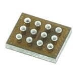
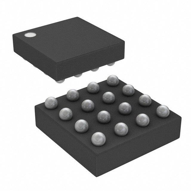
| 供应商器件封装 | 12-WLCSP (1.6x1.3) |
| 关闭 | Yes |
| 其它名称 | FTL75939UCXCT |
| 内部定时器数量 | 1 |
| 内部开关 | 是 |
| 包装 | 剪切带 (CT) |
| 单位重量 | 63 mg |
| 商标 | Fairchild Semiconductor |
| 安装类型 | 表面贴装 |
| 安装风格 | SMD/SMT |
| 封装 | Reel |
| 封装/外壳 | 12-UFBGA,WLCSP |
| 封装/箱体 | WLCSP-12 |
| 工作温度 | -40°C ~ 85°C |
| 工厂包装数量 | 3000 |
| 最大功率耗散 | 0.41 W |
| 最大工作温度 | + 85 C |
| 最小工作温度 | - 40 C |
| 标准包装 | 1 |
| 电压-输入 | 1.2 V ~ 5.5 V |
| 电流限制 | 4.5A |
| 电源电压-最大 | 5.5 V |
| 电源电压-最小 | 1.2 V |
| 电源电流 | 5 uA |
| 类型 | Timer |
| 系列 | FTL75939 |
| 输出数 | 1 |


- 商务部:美国ITC正式对集成电路等产品启动337调查
- 曝三星4nm工艺存在良率问题 高通将骁龙8 Gen1或转产台积电
- 太阳诱电将投资9.5亿元在常州建新厂生产MLCC 预计2023年完工
- 英特尔发布欧洲新工厂建设计划 深化IDM 2.0 战略
- 台积电先进制程称霸业界 有大客户加持明年业绩稳了
- 达到5530亿美元!SIA预计今年全球半导体销售额将创下新高
- 英特尔拟将自动驾驶子公司Mobileye上市 估值或超500亿美元
- 三星加码芯片和SET,合并消费电子和移动部门,撤换高东真等 CEO
- 三星电子宣布重大人事变动 还合并消费电子和移动部门
- 海关总署:前11个月进口集成电路产品价值2.52万亿元 增长14.8%


PDF Datasheet 数据手册内容提取
Is Now Part of To learn more about ON Semiconductor, please visit our website at www.onsemi.com Please note: As part of the Fairchild Semiconductor integration, some of the Fairchild orderable part numbers will need to change in order to meet ON Semiconductor’s system requirements. Since the ON Semiconductor product management systems do not have the ability to manage part nomenclature that utilizes an underscore (_), the underscore (_) in the Fairchild part numbers will be changed to a dash (-). This document may contain device numbers with an underscore (_). Please check the ON Semiconductor website to verify the updated device numbers. The most current and up-to-date ordering information can be found at www.onsemi.com. Please email any questions regarding the system integration to Fairchild_questions@onsemi.com. ON Semiconductor and the ON Semiconductor logo are trademarks of Semiconductor Components Industries, LLC dba ON Semiconductor or its subsidiaries in the United States and/or other countries. ON Semiconductor owns the rights to a number of patents, trademarks, copyrights, trade secrets, and other intellectual property. A listing of ON Semiconductor’s product/patent coverage may be accessed at www.onsemi.com/site/pdf/Patent-Marking.pdf. ON Semiconductor reserves the right to make changes without further notice to any products herein. ON Semiconductor makes no warranty, representation or guarantee regarding the suitability of its products for any particular purpose, nor does ON Semiconductor assume any liability arising out of the application or use of any product or circuit, and specifically disclaims any and all liability, including without limitation special, consequential or incidental damages. Buyer is responsible for its products and applications using ON Semiconductor products, including compliance with all laws, regulations and safety requirements or standards, regardless of any support or applications information provided by ON Semiconductor. “Typical” parameters which may be provided in ON Semiconductor data sheets and/or specifications can and do vary in different applications and actual performance may vary over time. All operating parameters, including “Typicals” must be validated for each customer application by customer’s technical experts. ON Semiconductor does not convey any license under its patent rights nor the rights of others. ON Semiconductor products are not designed, intended, or authorized for use as a critical component in life support systems or any FDA Class 3 medical devices or medical devices with a same or similar classification in a foreign jurisdiction or any devices intended for implantation in the human body. Should Buyer purchase or use ON Semiconductor products for any such unintended or unauthorized application, Buyer shall indemnify and hold ON Semiconductor and its officers, employees, subsidiaries, affiliates, and distributors harmless against all claims, costs, damages, and expenses, and reasonable attorney fees arising out of, directly or indirectly, any claim of personal injury or death associated with such unintended or unauthorized use, even if such claim alleges that ON Semiconductor was negligent regarding the design or manufacture of the part. ON Semiconductor is an Equal Opportunity/Affirmative Action Employer. This literature is subject to all applicable copyright laws and is not for resale in any manner.
F T L 7 5 9 May 2014 3 9 — C o FTL75939 n f i g Configurable Reset Timer with Integrated Load Switch u r a b l Features Description e R Factory Programmed Reset Delay: 7.5 s The FTL75939 is both a timer for resetting a mobile device es and an advanced load management switch for applications e Factory Programmed Reset Pulse: 400 ms requiring a highly integrated solution. t T Factory Customized Turn-on Time: 2.3 s If the mobile device is off, holding /SR0 LOW (by pressing im e Factory Customized Turn-off Delay: 7.3 s power-on key) for 2.3 s ±20% turns on the PMIC. r w Adjustable Reset Delay Option with External Resistor As a reset timer, it has one input and one fixed delay output. ith It generates a fixed delay of 7.5 s ±20% by disconnecting the Low ICCT Saves Power Interfacing to Low-Voltage Chips PMIC from the battery power supply for 400 ms ±20%. Then Int Off Pin Turns Off Load Switch to Maintain Battery the load switch is turned on again to reconnect the battery to eg the PMIC such that PMIC goes into power-on sequence. The r Charge during Shipment and Inventory. Ready to use a reset delay can be customized by connecting an external t Right Out of the Box e resistor to the DELAY_ADJ pin. Refer to Table 4. d Input Voltage Operating Range: 1.2 V to 5.5 V L As an advanced load management switch, the FTL75939 o Over-Voltage Protection: Allow Input Pins > VBAT disconnects loads powered from the DC power rail (<6 V) ad Typical R : 21 mΩ (Typ.) at V =4.5 V with stringent off-state current targets and high load S ON BAT capacitances (up to 200 µF). The FTL75939 consists of a w Slew Rate / Inrush Control with tR: 2.7 ms (Typical) slew-rate controlled low-impedance MOSFET switch (21 mΩ itc 3.8 A / 4.5 A Maximum Continuous Current (JEDEC tdyrpaiicna (l <a0t. 24 .µ5A V T) ythpaicta hl)a tso efaxccieliptatitoen caollmy ploliwan ocfef- swtiathte sctaunrrdebnyt h 2S2P, No VIA / with Thermal VIA) power requirements. The slew-rate-controlled turn-on Output Capacitor Discharge Function characteristic prevents inrush current and the resulting Zero-Second Test-Mode Enable excessive voltage drop on power rails. Low < 0.2 µA Typical Shutdown Current The low ICCT enables direct interface to lower-voltage chipsets without external translation, while maintaining low IEC61000-4-2, , Level 4 compliant SYS_WAKE Pin power consumption. ESD Protected: The device is packaged in advanced, fully green, 1.31 mm x - 8 kV HBM ESD (per JESD22-A114) 1.62 mm, Wafer-Level Chip-Scale Packaging (WLCSP) with - 10 kV HBM ESD (Pin to Pin, V & V ) backside laminate; providing excellent thermal conductivity, BAT OUT - 2 kV CDM (per JESD22-C101) small footprint, and low electrical resistance for a wide application range. Applications Related Resources Smart Phones, Tablet PCs For additional information, please contact: Storage, DSLR, and Portable Devices http://www.fairchildsemi.com/cf/#Regional-Sales Ordering Information Top Operating Part Number Package Packing Method Mark Temperature Range 12-Ball WLCSP (with backside laminate), 3000 Units on FTL75939UCX UA -40 to +85°C 3x4 Array, 0.4 mm Pitch, 250 µm Ball, Tape and Reel Nominal: 1.31 mm x 1.62 mm © 2012 Fairchild Semiconductor Corporation www.fairchildsemi.com FTL75939 • Rev. 1.0.2
F Application Diagram T L 7 VBUS VBUS SW 59 3 9 RSENSE — Switching VOUT Charger IC C Battery o e.g. FAN540x n VBAT VBAT VOUT fig u r DELAY_ADJ DSR GPIO or VBAT a b FTL75939 PMIC Baseband l RPU GPIO e OFF SYS_WAKE System Reset R RPD e s /SR0 GND e t T PHONE_ON_N im e r Power Key w i t h I Charger_In n Wake_1 OR t Wake_2 eg Figure 1. Typical Application with Stand Alone Switching Charger IC r a t e d L o USB Connector ger a Over Voltage ar d Protection ery Ch VPH_PWR Sw Batt itc DC Jack FOEPTVs OPvroetre Vcotioltang 2e Mode h h- c wit S VBAT PMIC with Integrated 1 VBAT VOUT 5 GPIO Charger m 2 OFF DELAY_ADJ 6 ste RPD FTL75939 y S ng Power_On 3 /SR0 SYS_WAKE 7 ori Monit RPU GPIO or VBAT 4 DSR GND 8 y er att B Battery Charger IN Event 1 OR Event 2 Power Key Figure 2. Typical Application PMIC with Integrated Charger © 2012 Fairchild Semiconductor Corporation www.fairchildsemi.com FTL75939 • Rev. 1.0.2 2
Functional Block Diagram F T L VBAT VOUT 7 5 Turn-On Slew Rate 9 Controlled Driver 3 9 Voltage — Reference C Output o Discharge n Oscillator f OFF DELAY_ADJ ig u r a /SR0 VBAT b l Digital Logic & e DSR Counter SYS_WAKE R e s e t T im e r w i t GND h I n Figure 3. Block Diagram te g Pin Configuration ra t e d A1 A2 A3 A3 A2 A1 Lo a d B1 B2 B3 B3 B2 B1 S w i t c C1 C2 C3 C3 C2 C1 h D1 D2 D3 D3 D2 D1 Figure 4. Top View Figure 5. Bottom View Pin Definitions Description Pin # Name Normal Operation 0-Second Factory-Test Mode(1) A1, A2, A3 V Switch Output Switch Output OUT B1, B2, B3 V Supply Input Supply Input BAT C1 GND Ground Ground Delay selection input; connected to GPIO with 100 K pull-up C2 DSR Logic LOW or to V directly without pull-up resistor BAT C3 /SR0 Power-on or reset input; active LOW. Logic LOW Reset delay adjustment; MUST tie to V directly if not BAT D1 DELAY_ADJ used. To adjust the reset delay, a resistor (R ) is Connected to V or GND ADJ BAT connected between this pin and ground Load switch disable; Rising Edge Triggered; changes load D2 OFF Don’t Care switch from ON state to OFF state. System wake-up input; changes load switch from OFF state D3 SYS_WAKE Don’t Care to ON state Note: 1. 0-Second Factory Test Mode is for t and t only. VON PHL1 © 2012 Fairchild Semiconductor Corporation www.fairchildsemi.com FTL75939 • Rev. 1.0.2 3
Absolute Maximum Ratings F T Stresses exceeding the absolute maximum ratings may damage the device. The device may not function or be operable L above the recommended operating conditions and stressing the parts to these levels is not recommended. In addition, 7 5 extended exposure to stresses above the recommended operating conditions may affect device reliability. The absolute 9 3 maximum ratings are stress ratings only. 9 — Symbol Parameters Condition Min. Max. Unit C o VBAT VBAT to GND n -0.3 6.5 V f VOUT VOUT to GND ig u 2S2P JEDEC std. PCB 3.8 r a ISW Maximum Continuous Switch Current A b 2S2P + Thermal VIA JEDEC std. PCB 4.5 l e P Power Dissipation I =4.5 A, R = 20 mΩ (max) 0.41 W R D OUT ON e /SR0, DSR, OFF, DELAY_ADJ -0.5 6.5 s e V DC Input Voltage V IN SYS_WAKE(2) VBAT+0.3 t T I DC Input Diode Current V < 0 V -50 mA im IK BAT e ICC DC VCC or Ground Current per Supply Pin 100 mA r w TSTG Storage Temperature Range -65 +150 C ith TJ Junction Temperature Under Bias +150 C In t e TL Junction Lead Temperature, Soldering 10 Seconds +260 C g r 2S2P JEDEC std. PCB 86 a JA Thermal Resistance, Junction-to-Ambient °C/W te 2S2P + Thermal VIA JEDEC std. PCB 48 d L Thermal Resistance, Junction-to-Case(3) 10.9 °C/W o JC a d Human Body Model, JEDEC: JESD22-A114 All Pins 8 S Human Body Model, Pin to Pin(4) V , V 10 w BAT OUT i t c ESD IEC 61000-2-4, Level 4, for SYS_WAKE(5) Air 15 kV h Contact 8 Charged Device Model, JESD22-C101 2 Notes: 2. SYS_WAKE operates up to 28 V if an external resistor is attached. A value of 100 kΩ is typically recommended. 3. Uniform temperature at bottom solder. 4. Test conditions: V vs. GND and V vs. GND. BAT OUT 5. A 100 kΩ resistor is required between SYS_WAKE and USB Charger In. Recommended Operating Conditions The Recommended Operating Conditions table defines the conditions for actual device operation. Recommended operating conditions are specified to ensure optimal performance to the datasheet specifications. Fairchild does not recommend exceeding them or designing to Absolute Maximum Ratings. Symbol Parameters Condition Min. Max. Unit V V 1.2 BAT BAT 5.5 Input Voltage(6) /SR0, DSR, OFF 0 V V IN SYS_WAKE 0 V BAT V Output Voltage 0 5.5 V OUT t V Recovery Time After Power Down V =0 V After Power Down, Rising to 0.5 V 5 ms RFC BAT BAT TA Free-Air Operating Temperature -40 +85 C Note: 6. V should never be allowed to float while input pins are driven. BAT © 2012 Fairchild Semiconductor Corporation www.fairchildsemi.com FTL75939 • Rev. 1.0.2 4
F T Electrical Characteristics L 7 5 Unless otherwise noted, V =1.2 to 5.5 V and T =-40 to +85°C; typical values are at V =4.5 V and T =25°C. 9 BAT A BAT A 3 9 Symbol Parameters Conditions Min. Typ. Max. Unit — C Basic Operation o n IOFF Off Supply Current VBAT=4.5 V, VOUT=Open, Load Switch=OFF 5.5 μA fi g V =4.5 V, V =GND, Load Switch=OFF 0.2 5.5 u BAT OUT I Shutdown Current μA r SD a VBAT=3.8 V, VOUT=GND, Load Switch=OFF 0.1 4.5 b l V =5.5 V, I =1 A(7) 20 24 e BAT OUT R V =4.5 V, I =1 A, T =25°C(7) 21 25 e BAT OUT A s RON On Resistance VVBBAATT==32..35 VV,, IIOOUUTT==550000 mmAA((77)) 2248 2395 mΩ et Tim V =1.8 V, I =250 mA(7) 37 45 e BAT OUT r V =1.2 V, I =250 mA, T =25°C(7) 75 100 w BAT OUT A i t V =4.5 V, V = OFF, I =20 mA, h RPD Output Discharge RPULL DOWN TAB=AT25°C OUT FORCE 65 85 Ω In t e VIH Input High Voltage(8) 11..28 VV<VVBBAATT15..85 VV 11..02 VV grat e V Input Low Voltage(8) 0.45 V d IL L o IIN Input Leakage Current(8) 0 V VBAT 5.5 V 1.5 μA a d /SR0=5.5 V, DSR=5.5 V, S w SYS_WAKE=5.5 V, OFF =GND, IOUT=0 mA, 5 7 it V =5.5 V, Load Switch=ON c I BAT μA h CCQ /SR0=3.8 V, DSR=3.8 V, Quiescent Current SYS_WAKE=3.8 V, OFF=GND, I =0 mA, 4 5.5 OUT V =3.8 V, Load Switch=ON BAT /SR0=1.2 V or DSR=1.2 V or OFF=1.2 V, I SYS_Wake=1.2 V, V =5.5 V, Load 7 12 μA CCT BAT Switch=ON /SR0=GND, DSR=5.5 V, V =5.5 V, Load I Dynamic Supply Current BAT 60 μA CC Switch=ON Notes: 7. This parameter is guaranteed by design and characterization; R is tested with different voltage and current ON conditions in production. 8. Input pins are /SR0, OFF, DSR, and SYS_WAKE. Input pins should not be floated when V is connected to the BAT power supply. © 2012 Fairchild Semiconductor Corporation www.fairchildsemi.com FTL75939 • Rev. 1.0.2 5
AC Electrical Characteristics F T Unless otherwise noted, VBAT=1.2 to 5.5 V and TA=-40 to +85°C; typical values are at VBAT=4.5 V and TA=25°C. L 7 5 Symbol Parameter Conditions Min. Typ. Max. Unit 9 3 9 Power-On and Reset Timing — t Turn-On Time for V CL=5 pF, RL=5 kΩ, DSR=HIGH, 1.8 2.3 2.8 s C VON OUT Figure 30 o n t Timer Delay before Reset CL=5 pF, RL=5 kΩ, DSR=HIGH, 6.0 7.5 9.0 s fig PHL1 Figure 31 u r a tREC1 Reset Timeout Delay of VOUT CL=5 pF, RL=5 kΩ, Figure 31 320 400 480 ms b l e Load Switch Turn-On Timing R e t Turn-On Delay(9) 1.7 ms s DON e tR VOUT Rise Time(9) VTB=AT2=54°.C5, VF,i gRuLr=e5 2 Ω9 , CL=100 µF, 2.7 ms t T t Turn-On Time(9), SYS_WAKE to V A 4.4 ms im ON OUT e Load Switch Turn-Off with Delay r w tSD Delay to Turn Off Load Switch 5.8 7.3 8.8 s ith t V Fall Time(9) VBAT=4.5 V, RL=150 Ω, CL=100 µF, 10.0 ms I F OUT T =25°C, DSR=HIGH, Figure 28 n t Turn-Off(10,11) A 7.3 s te OFF g r Load Switch Zero-Second Turn-Off a t e t Delay to Turn Off Load Switch 0.6 ms d SD tF VOUT Fall Time(9) VTB=AT2=54°.C5, VD,S RRL==L1O50W Ω, ,F CigLu=r1e0 208 µ F, 10.0 ms Lo A a t Turn-Off(10,11) 10.6 ms d OFF S Notes: w 9. t =t + t . i ON R DON t c 10. tOFF=tF + tSD. h 11. Output discharge enabled during off-state. Zero-Second Factory Test Mode Unless otherwise noted, V =1.2 to 5.5 V and T =-40 to +85°C; typical values are at V =4.5 V and T =25°C. BAT A BAT A Symbol Parameter Conditions Min. Typ. Max. Unit C =5 pF, R =5 kΩ, V =OFF, t Turn-On Time for V L L OUT 4 ms VON OUT DSR=LOW, Figure 30 C =5 pF, R =5 kΩ, V =ON, t Timer Delay before Reset L L OUT 1 ms PHL1 DSR=LOW, Figure 31 © 2012 Fairchild Semiconductor Corporation www.fairchildsemi.com FTL75939 • Rev. 1.0.2 6
Typical Characteristics F T L 7 5 9 3 9 — C o n f i g u r a b l e R e s Figure 6. Shutdown Current vs. Temperature Figure 7. Shutdown Current vs. Supply Voltage e t T im e r w i t h I n t e g r a t e d L o a d Figure 8. Off Supply Current vs. Temperature Figure 9. Off Supply Current vs. Supply Voltage S (VOUT=0 V) (VOUT=0 V) w i t c h Figure 10. Quiescent Current vs. Temperature Figure 11. Quiescent Current vs. Supply Voltage Figure 12. Quiescent Current vs. On Voltage (V =4.5 V) Figure 13. Quiescent Current vs. On Voltage (V =5.5 V) BAT BAT © 2012 Fairchild Semiconductor Corporation www.fairchildsemi.com FTL75939 • Rev. 1.0.2 7
Typical Characteristics F T L 7 5 9 3 9 — C o n f i g u r a b l e R e s Figure 14. Output Discharge Resistor RPD Figure 15. Output Discharge Resistor RPD vs. e vs. Temperature Supply Voltage t T im e r w i t h I n t e g r a t e d L o a d S Figure 16. RON vs. Temperature Figure 17. RON vs. Supply Voltage w i 100 tc h A) 10 T ( N 1ms E R R U 1 C AIN RDS(ON)LIMIT 11000mmss DR SINGLE PULSE 1s , D0.1 RqJA= 238oC/W 10s I T = 25oC DC A 0.01 0.01 0.1 1 10 VDS, DRAIN-SOURCE VOLTAGE (V) Figure 18. t /t vs. Temperature Figure 19. I vs. (V -V ) — SOA R F SW IBAT OUT Figure 20. t /t vs. Temperature Figure 21. t vs. Supply Voltage R DON R © 2012 Fairchild Semiconductor Corporation www.fairchildsemi.com FTL75939 • Rev. 1.0.2 8
Typical Characteristics F T L 4.5 7 5 4 9 3 9 3.5 — 3 C o Voltage (V)2.52 +25C nfig u 1.5 r a b 1 l e 0.5 VON R e 0 s 0 5 10 15 20 25 30 35 e Time (ms) t Figure 22. tR vs. Supply Voltage Figure 23. Turn-Off Response (VBAT=4.5 V, CIN=10 µF, T CL=100 µF, without External RL) im e r w i t h I n t e g r a t e d L o a d S w i t c h Figure 24. Turn-On Response (V =4.5 V, C =10 µF, Figure 25. Turn-On Response (V =4.5 V, C =10 µF, BAT IN BAT IN C =1 µF, R =50 ) C =100 µF, R =5 ) L L L L 100 10.000 10 1.000 100mF 500 1 50 T(ms)FALL0.100 10mF T(ms)FALL 0.1 5 0.010 1mF 0.01 0.001 0.001 1 10 RLOA1D0(0) 1000 10000 0.1 1 CLOA1D0(mF) 100 1000 Figure 26. Fall Time as a Function of External Resistive Figure 27. Fall Time as a Function of External Capacitive Load (CL=1 µF, 10 µF, and 100 µF) Load (RL=5 , 50 , and 500 ) © 2012 Fairchild Semiconductor Corporation www.fairchildsemi.com FTL75939 • Rev. 1.0.2 9
F Application Information T L 7 Reset Timer and Advanced Load Management Reset Timer 5 9 During normal operation of a mobile device, if a reset 3 The FTL75939 is both a reset IC and an advanced load 9 operation is needed for mobile equipmen;, holding the power management device. A typical application is shown in — switch, to which /SR0 is connected and is forced LOW, for at Figure 1. least 7.5 s, causes the FTL75939 to cut off the supply power C o Disconnect PMIC from Battery (Turn Off) to PMIC for 400 ms by turning off the load switch. The n After holding the DSR pin HIGH, changing the OFF pin from FTL75939 then automatically turns on the load switch to fi g LOW to HIGH (rising edge triggered) and holding it HIGH for reconnect the PMIC to battery. This forces PMIC to enter a u at least 1 ms; the FTL75939 triggers an internal counter to power-on sequence. ra allow a factory-customized 7.3 s delay before turning off b internal load switch. The delay is intended to allow the PMIC If the power switch is released and /SR0 is returned to HIGH le to complete a power-down sequence before safely within 7.5 s, the FTL75939 resets its counter and VOUT R remains in ON state; there is no change on V and a reset e disconnecting from the power supply. However, the turn-off OUT s does not occur. e sequence is terminated if a higher priority input is detected in t tSD period (see Resolving Input Conflicts). Power-On Reset Tim When FTL75939 is connected to a battery (V ≥ 1.2 V), the Alternatively, after holding the DSR pin LOW, changing the BAT e OFF pin from LOW to HIGH (rising edge triggered) and part enters Power-On Reset (POR) Mode. All internal r registers are reset and V is ON at the end of POR w holding it HIGH for at least 1 ms; the FTL75939 triggers the sequence (see 0). OUT it zero-second turn-off. Delay t is significantly reduced to h 0.6 ms to avoid the default delaSyD to turn-off load switch (tSD). Zero-Second Factory Test Mode In t e With its stringent shutdown current flow, the FTL75939 FTL75939 includes a Zero-Second Factory Test Mode to g significantly reduces the current drain on a battery when the shorten the turn-on time for VOUT (tVON) and timer delay ra PMIC is turned off. This preserves the battery power for a before reset (tPHL1) for factory testing. te longer period when a mobile device is in Shutdown Mode. d When VOUT is OFF, the default turn-on time (tVON) is 2.3 s. If L Power On the DSR pin is LOW prior to /SR0 going LOW, the FTL75939 o a There are two methods to turn on the load switch to wake up bypasses the 2.3 s delay and V changes from OFF to ON d OUT the PMIC. When a HIGH is inserted to the SYS_WAKE pin immediately. S w or when /SR0 is held LOW for > 2.3 s (see Figure 30); the FTL75939 turns on its load switch to allow PMIC to connect Similiarly, default reset delay (tPHL1) is 7.5 s. If VOUT is ON itc to the battery. The reset feature is disabled when V is and the DSR pin is LOW prior to /SR0 going LOW, the h OUT FTL75939 enters Zero-Second Factory Test Mode and toggled from OFF to ON. Continuously holding /SR0 LOW bypasses the default reset delay of 7.5 s; V is pulled from does not trigger a reset event. OUT ON to OFF immediately. The reset pulse (t ) remains at REC1 To enable the reset feature, /SR0 must return to HIGH such 400 ms in Zero-Second Factory Test Mode. that FTL75939 resets its internal counter. DSR should never be left floating during normal operation. Table 1. V and Input Conditions OUT Initial Conditions (t=0 Second) V OUT Associated Delay Function /SR0 SYS_WAKE OFF DSR Before After LOW X(12) X LOW t < 4 ms OFF ON VON Power-On LOW X X HIGH t =2.3 s OFF ON VON HIGH HIGH X X t =4.4 ms OFF ON ON t < 1 ms LOW X X LOW t PHL1=400 ms ON (12) REC1 Reset Function t =7.5 s(13) LOW X X HIGH PHL1 ON tREC1=400 ms HIGH LOW LOW t < 1 ms ON OFF SD (12) Turn Off HIGH LOW HIGH t =7.3 s ON OFF SD Notes: 12. X=Don’t Care, = Rising Edge, =HIGH to LOW to HIGH. 13. Reset delay (t ) is adjustable (seeTable 4). PHL1 © 2012 Fairchild Semiconductor Corporation www.fairchildsemi.com FTL75939 • Rev. 1.0.2 10
F Table 2. Pin Condition after POR T L Pin Name /SR0 DSR SYS_WAKE OFF VOUT 7 5 9 Default State (after POR) 1 1 0 0 ON 3 9 Note: — 14. 1=Input Logic HIGH, 0=Input Logic LOW, ON=load switch is ON state. C o n Timing Diagrams fi g u tOFF tON ra b tSD le R 50% e s OFF 50% e t T ` SYS_WAKE im 90% e r w VOUT 10% ith 90% V I OUT n tR t e 10% g t r tF DON at e d Figure 28. Timing Diagram (OFF vs. VOUT) Figure 29. Timing Diagram (SYS_WAKE vs. VOUT) L o a d tVON S w /SR0 tPHL1 itc h 50% /SR0 tREC1 50% V OUT 50% 50% 50% V OUT Figure 30. Power On with /SR0 Figure 31. Reset Timing Special Note on OFF Pin Resolving Input Conflicts In the t period (DSR=HIGH only, see Figure 28); if /SR0 or SD The FTL75939 allows multiple simultaneous inputs and can SYS_WAKE is triggered when 0 < t < t , the FTL75939 SD resolve conflicts based on priority level (see Table 3). When exits the turn-off sequence and V remains in ON state. OUT two input pins are triggered at the same time, only the higher The higher priority input is served regardless of the condition priority input is served and the lower priority input is ignored. of OFF pin. The lower-priority signal must be repeated to be serviced. To re-initiate the turn-off sequence, the OFF pins must return Table 3. Input Priority to LOW, then toggle from LOW to HIGH again. The same input priority applies (Table 3) if DSR = HIGH. Input Priority (1=Highest) Special Note on SYS_WAKE Pin /SR0 1 The SYS_WAKE pin is designed and characterized to SYS_WAKE 2 handle high voltage input: at least 20 V. Therefore, in application, a current-limiting resistor (i.e 100 kΩ) is required OFF 3 between SYS_WAKE and the input signal regardless of input voltage. © 2012 Fairchild Semiconductor Corporation www.fairchildsemi.com FTL75939 • Rev. 1.0.2 11
F Adjustable Reset Delay with an External Fall Time T L Resistor and DSR Device output fall time can be calculated based on the RC 7 5 constant of the external components, as follows: 9 The reset delay is adjustable by connecting a commonly 3 9 abveatwilaebelne ,t hel oDwE-pLoAwYe_rA, DJ± p5i%n ,a ndR othHeS G-cNomD ppliiann (t seere Tsiasbtoler tF RLCL2.2 (1) — 4). To disable the adjustable delay feature, DELAY_ADJ where tF is 90% to 10% fall time; RL is output load; and CL C is output capacitor. o should be tied to V directly. BAT n The reset delay is factory programmed at 7.5 s. The same equation works for a device with a pull-down output fig resistor. RL is replaced by a parallel connected pull-down and u The additional power consumption caused by using an an external output resistor combination, calculated as: ra external resistor is negligible. The external resistor is b n/SoRrm0 aisll yp udlilsecdo LnnOeWct.e d and is enabled for milliseconds when tF RRLRRPD CL2.2 (2) le R L PD e s where t is 90% to 10% fall time; R is output load; This external adjustment feature provides a simple alternate F L e method for controlling delay time for engineering and RPD=65 is output pull-down resistor; and CL is the t T production at customer’s location. output capacitor. im Fairchild can also factory program a wide range of turn-on Resistive Output Load er times for VOUT (tVON), timer delay before reset (tPHL1), reset If resistive output load is missing, the IntelliMAX switch w i timeout delay for VOUT (tREC1), and load switch turn-off time without a pull-down output resistor does not discharge the th (tOFF) to match customer applications. In this case, the output voltage. Output voltage drop depends, in that case, In external resistor (RADJ) can be eliminated. mainly on external device leaks. te g For more details, contact an authorized sales representative: r a http://www.fairchildsemi.com/cf/#Regional-Sales. t e Application Specifics d L Table 4. Delay Adjustment vs. External Resistor o At maximum operational voltage (VBAT=5.5 V), device inrush a Adjusted Reset current might be higher than expected. Spike current should d External Resistor Delay be taken into account if V >5 V and the output capacitor is S Delay t _ADJ, BAT w RADJ (kΩ) Multiplier (SecondPsHL)1 ±20% much larger than the input capacitor. Input current IBAT can it be calculated as: c h Tie to GND 0.50 x t 3.8 (No Resistor) PHL1 I (t)VOUT(t)(C C )dVOUT(t) (3) BAT R LOAD IN dt 3.9 0.75 x t 5.6 LOAD PHL1 where switch and wire resistances are neglected and 10 1.25 x t 9.4 PHL1 capacitors are assumed ideal. 22 1.50 x t 11.3 PHL1 Estimating V (t)=V /10 and using experimental formula OUT BAT 47 1.75 x tPHL1 13.1 for slew rate (dVOUT(t)/dt), spike current can be written as: 120 2.00 x tPHL1 15.0 maxI VBAT C C 0.05V 0.255 (4) Tie to V BAT 10R LOAD IN BAT BAT 1.00 x t 7.5 LOAD (No Resistor) PHL1 where supply voltage V is in volts; capacitances are in BAT micro farads; and resistance is in ohms. Example: If V =5.5 V, C =100 µF, C =10 µF, and BAT LOAD IN IntelliMAX™ Switch Inside the FTL75939 R =50 ; calculate the spike current by: LOAD 5.5 Input Capacitor max(I ) (10010)(0.055.50.255)A1.8A BAT 1050 The IntelliMAX™ switch inside the reset timer doesn’t Maximum spike current is 1.8 A, while average ramp-up require an input capacitor. To reduce device inrush current, current is: a 0.1 µF ceramic capacitor, C , is recommended close to IN the VBAT pin. A higher value of CIN can be used to reduce the I (t)VOUT(t)(C C )dVBAT(t) voltage drop experienced as the switch is turned on into a BAT RLOAD LOAD IN dt large capacitive load. 2.75/501000.00220.275A Output Capacitor Output Discharge While the load switch works without an output capacitor; if The device contains a RPD=65 Ω on-chip pull-down resistor parasitic board inductance forces V below GND when for quick output discharge. The resistor is activated when the OUT switching off, a 0.1 µF capacitor, C , should be placed switch is turned off. OUT between V and GND. OUT © 2012 Fairchild Semiconductor Corporation www.fairchildsemi.com FTL75939 • Rev. 1.0.2 12
Recommended Layout F T L For best thermal performance and minimal inductance and C1 (GND) is connected to GND plane of PCB. 7 parasitic effects, keeping the input and output traces short 5 and capacitors as close to the device as possible is Reserve a pad for capacitor connection (C1) between 93 recommended. Additional recommended layout VBAT and GND, if no input capacitor is planned. 9 — considerations include: Reserve a pad for capacitor connection (C2) between C V and GND, if no output capacitor is planned. A1, A2, and A3 are interconnected at PCB, as close to OUT o the landing pad as possible. Use a dedicated VOUT or VBAT plane to improve thermal nfi dissipation. g B1, B2, and B3 are interconnected at PCB, as close to u r the landing pad as possible. a b le R e s e t T im e r w i t h I n t e g r a t e d L o a d S w i t c h Figure 32. Sample Layout © 2012 Fairchild Semiconductor Corporation www.fairchildsemi.com FTL75939 • Rev. 1.0.2 13
F Physical Dimensions T L 7 5 9 3 9 0.03 C F — 2X E A 0.80 (Ø0.200) B Cu Pad C o n f i 1.20 0.40 (Ø0.300) g u PIN 1 AREA D Solder Mask ra b 0.40 le 0.03 C R e 2X s e TOP VIEW RECOMMENDED LAND PATTERN t (NSMD PAD TYPE) T im e r w 0.625 0.378±0.018 it 0.05 C 0.547 0.208±0.021 h I n t e g C SEATING PLANE r D a t SIDE VIEWS e d L o a 0.005 C A B NOTES: d 0.80 S Ø0.260±0.02 A. NO JEDEC REGISTRATION APPLIES. w 0.40 12X i t B. DIMENSIONS ARE IN MILLIMETERS. c D h C C. DIMENSIONS AND TOLERANCES PER 1.20 0.40 B (Y)±0.018 ASME Y14.5M, 1994. A F D. DATUM C IS DEFINED BY THE SPHERICAL 1 2 3 CROWNS OF THE BALLS. (X)±0.018 E. PACKAGE NOMINAL HEIGHT IS 586 MICRONS ±39 MICRONS (547-625 MICRONS). BOTTOM VIEW F. FOR DIMENSIONS D, E, X, AND Y SEE PRODUCT DATASHEET. G. DRAWING FILENAME: MKT-UC012ACrev1. Figure 33. 12-Ball, Wafer-Level Chip-Scale Packaging (WLCSP) 3x4 Array, 0.4 mm Pitch, 250 µm Ball D E X Y 1.615 ±0.030 1.310 ±0.030 0.255 0.208 Package drawings are provided as a service to customers considering Fairchild components. Drawings may change in any manner without notice. Please note the revision and/or date on the drawing and contact a Fairchild Semiconductor representative to verify or obtain the most recent revision. Package specifications do not expand the terms of Fairchild’s worldwide terms and conditions, specifically the warranty therein, which covers Fairchild products. Always visit Fairchild Semiconductor’s online packaging area for the most recent package drawings: http://www.fairchildsemi.com/dwg/UC/UC012AC.pdf. For current packing container specifications, visit Fairchild Semiconductor’s online packaging area: http://www.fairchildsemi.com/packing_dwg/PKG-UC012AC.pdf. © 2012 Fairchild Semiconductor Corporation www.fairchildsemi.com FTL75939 • Rev. 1.0.2 14
F T L 7 5 9 3 9 — C o n f i g u r a b l e R e s e t T im e r w i t h I n t e g r a t e d L o a d S w i t c h © 2012 Fairchild Semiconductor Corporation www.fairchildsemi.com FTL75939 • Rev. 1.0.2 15
ON Semiconductor and are trademarks of Semiconductor Components Industries, LLC dba ON Semiconductor or its subsidiaries in the United States and/or other countries. ON Semiconductor owns the rights to a number of patents, trademarks, copyrights, trade secrets, and other intellectual property. A listing of ON Semiconductor’s product/patent coverage may be accessed at www.onsemi.com/site/pdf/Patent−Marking.pdf. ON Semiconductor reserves the right to make changes without further notice to any products herein. ON Semiconductor makes no warranty, representation or guarantee regarding the suitability of its products for any particular purpose, nor does ON Semiconductor assume any liability arising out of the application or use of any product or circuit, and specifically disclaims any and all liability, including without limitation special, consequential or incidental damages. Buyer is responsible for its products and applications using ON Semiconductor products, including compliance with all laws, regulations and safety requirements or standards, regardless of any support or applications information provided by ON Semiconductor. “Typical” parameters which may be provided in ON Semiconductor data sheets and/or specifications can and do vary in different applications and actual performance may vary over time. All operating parameters, including “Typicals” must be validated for each customer application by customer’s technical experts. ON Semiconductor does not convey any license under its patent rights nor the rights of others. ON Semiconductor products are not designed, intended, or authorized for use as a critical component in life support systems or any FDA Class 3 medical devices or medical devices with a same or similar classification in a foreign jurisdiction or any devices intended for implantation in the human body. Should Buyer purchase or use ON Semiconductor products for any such unintended or unauthorized application, Buyer shall indemnify and hold ON Semiconductor and its officers, employees, subsidiaries, affiliates, and distributors harmless against all claims, costs, damages, and expenses, and reasonable attorney fees arising out of, directly or indirectly, any claim of personal injury or death associated with such unintended or unauthorized use, even if such claim alleges that ON Semiconductor was negligent regarding the design or manufacture of the part. ON Semiconductor is an Equal Opportunity/Affirmative Action Employer. This literature is subject to all applicable copyright laws and is not for resale in any manner. PUBLICATION ORDERING INFORMATION LITERATURE FULFILLMENT: N. American Technical Support: 800−282−9855 Toll Free ON Semiconductor Website: www.onsemi.com Literature Distribution Center for ON Semiconductor USA/Canada 19521 E. 32nd Pkwy, Aurora, Colorado 80011 USA Europe, Middle East and Africa Technical Support: Order Literature: http://www.onsemi.com/orderlit Phone: 303−675−2175 or 800−344−3860 Toll Free USA/Canada Phone: 421 33 790 2910 Fax: 303−675−2176 or 800−344−3867 Toll Free USA/Canada Japan Customer Focus Center For additional information, please contact your local Email: orderlit@onsemi.com Phone: 81−3−5817−1050 Sales Representative © Semiconductor Components Industries, LLC www.onsemi.com www.onsemi.com 1
Mouser Electronics Authorized Distributor Click to View Pricing, Inventory, Delivery & Lifecycle Information: O N Semiconductor: FTL75939UCX