ICGOO在线商城 > 集成电路(IC) > PMIC - 配电开关,负载驱动器 > TPS2024IDRQ1

 Datasheet下载
- 型号: TPS2024IDRQ1
- 制造商: Texas Instruments
- 库位|库存: xxxx|xxxx
- 要求:
| 数量阶梯 | 香港交货 | 国内含税 |
| +xxxx | $xxxx | ¥xxxx |
查看当月历史价格
查看今年历史价格
TPS2024IDRQ1产品简介:
ICGOO电子元器件商城为您提供TPS2024IDRQ1由Texas Instruments设计生产,在icgoo商城现货销售,并且可以通过原厂、代理商等渠道进行代购。 TPS2024IDRQ1价格参考¥6.73-¥15.15。Texas InstrumentsTPS2024IDRQ1封装/规格:PMIC - 配电开关,负载驱动器, 。您可以下载TPS2024IDRQ1参考资料、Datasheet数据手册功能说明书,资料中有TPS2024IDRQ1 详细功能的应用电路图电压和使用方法及教程。
TPS2024IDRQ1 是 Texas Instruments(德州仪器)生产的一款电源管理集成电路(PMIC),属于配电开关及负载驱动器类别。该器件主要用于实现对负载的高效、安全供电管理,广泛应用于汽车电子、工业控制、通信设备等领域。

其主要应用场景包括:

1. 汽车电子系统:如车载娱乐系统、车身控制模块、电动门窗控制等,TPS2024IDRQ1具备汽车级工作温度范围和可靠性,适合在复杂电磁环境和振动环境中稳定工作。

2. 工业自动化设备:用于控制电机、继电器、传感器、执行器等负载,实现对多个负载的独立供电管理,提升系统安全性和可维护性。

3. 通信设备:如基站、路由器、交换机等设备中的电源分配系统,用于控制和监测不同模块的供电状态,防止过载或短路造成的系统损坏。

4. 便携式设备与电源管理系统:在需要多路负载控制的场合,如电池供电系统中,实现对不同子系统的电源开关控制,提升能效与电池寿命。

该器件具备四路独立的高边开关,内置过流保护、过温保护、欠压锁定等功能,支持负载电流监测,适合需要高可靠性和智能化电源管理的设计需求。
| 参数 | 数值 |
| 产品目录 | 集成电路 (IC) |
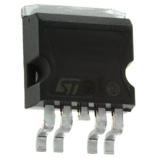
| 描述 | IC 3A PWR DIST SWITCH 8-SOIC |
| 产品分类 | PMIC - 电源分配开关 |
| 品牌 | Texas Instruments |
| 数据手册 | |
| 产品图片 |
|
| 产品型号 | TPS2024IDRQ1 |
| Rds(On) | 36 毫欧 |
| rohs | 无铅 / 符合限制有害物质指令(RoHS)规范要求 |
| 产品系列 | - |
| 供应商器件封装 | 8-SOIC |
| 其它名称 | 296-37977-1 |
| 内部开关 | 是 |
| 制造商产品页 | http://www.ti.com/general/docs/suppproductinfo.tsp?distId=10&orderablePartNumber=TPS2024IDRQ1 |
| 包装 | 剪切带 (CT) |
| 安装类型 | 表面贴装 |
| 封装/外壳 | 8-SOIC(0.154",3.90mm 宽) |
| 工作温度 | -40°C ~ 85°C |
| 开关类型 | 通用 |
| 标准包装 | 1 |
| 比率-输入:输出 | 1:1 |
| 特性 | - |
| 电压-负载 | 2.7 V ~ 5.5 V |
| 电压-输入 | 2.7 V ~ 5.5 V |
| 电流-输出(最大值) | 2A |
| 电流限制 | 3A |
| 类型 | 高端开关 |
| 输入类型 | 非反相 |
| 输出数 | 1 |
| 输出类型 | N 通道 |
| 配用 | /product-detail/zh/TPS2024EVM-290/296-31116-ND/1907503 |


- 商务部:美国ITC正式对集成电路等产品启动337调查
- 曝三星4nm工艺存在良率问题 高通将骁龙8 Gen1或转产台积电
- 太阳诱电将投资9.5亿元在常州建新厂生产MLCC 预计2023年完工
- 英特尔发布欧洲新工厂建设计划 深化IDM 2.0 战略
- 台积电先进制程称霸业界 有大客户加持明年业绩稳了
- 达到5530亿美元!SIA预计今年全球半导体销售额将创下新高
- 英特尔拟将自动驾驶子公司Mobileye上市 估值或超500亿美元
- 三星加码芯片和SET,合并消费电子和移动部门,撤换高东真等 CEO
- 三星电子宣布重大人事变动 还合并消费电子和移动部门
- 海关总署:前11个月进口集成电路产品价值2.52万亿元 增长14.8%


PDF Datasheet 数据手册内容提取
TPS2020-Q1, TPS2021-Q1 TPS2022-Q1, TPS2024-Q1 www.ti.com SGLS260G–SEPTEMBER2004–REVISEDJUNE2010 POWER-DISTRIBUTION SWITCHES CheckforSamples:TPS2020-Q1,TPS2021-Q1,TPS2022-Q1,TPS2024-Q1 FEATURES 1 • QualifiedforAutomotiveApplications • AmbientTemperatureRange:–40°Cto85°C • 33-mΩ (5-VInput)High-SideMOSFETSwitch • ESDProtection:2-kVHuman-BodyModel, • Short-CircuitandThermalProtection 200-VMachineModel • OvercurrentLogicOutput • ULListed-FileNo.E169910 • OperatingRange:2.7Vto5.5V D PACKAGE • Logic-LevelEnableInput (TOPVIEW) • TypicalRiseTime:6.1ms GND 1 8 OUT • UndervoltageLockout IN 2 7 OUT • MaximumStandbySupplyCurrent:10mA IN 3 6 OUT • NoDrain-SourceBack-GateDiode EN 4 5 OC • Availablein8-PinSOICPackage DESCRIPTION The TPS202x family of power distribution switches is intended for applications where heavy capacitive loads and short circuits are likely to be encountered. These devices are 50-mΩ N-channel MOSFET high-side power switches. The switch is controlled by a logic enable compatible with 5-V logic and 3-V logic. Gate drive is provided by an internal charge pump designed to control the power-switch rise times and fall times to minimize current surges during switching. The charge pump requires no external components and allows operation from suppliesaslowas2.7V. When the output load exceeds the current-limit threshold or a short is present, the TPS202x limits the output current to a safe level by switching into a constant-current mode, pulling the overcurrent (OC) logic output low. When continuous heavy overloads and short circuits increase the power dissipation in the switch, causing the junction temperature to rise, a thermal protection circuit shuts off the switch to prevent damage. Recovery from a thermal shutdown is automatic once the device has cooled sufficiently. Internal circuitry ensures the switch remainsoffuntilvalidinputvoltageispresent. The TPS202x devices differ only in short-circuit current threshold. The TPS2020 limits at 0.3-A load, the TPS2021 at 0.9-A load, the TPS2022 at 1.5-A load, and the TPS2024 at 3-A load. The TPS202x is available in an 8-pin small-outline integrated-circuit (SOIC) package and operates over a junction temperature range of –40°Cto125°C. 1 Pleasebeawarethatanimportantnoticeconcerningavailability,standardwarranty,anduseincriticalapplicationsofTexas Instrumentssemiconductorproductsanddisclaimerstheretoappearsattheendofthisdatasheet. PRODUCTIONDATAinformationiscurrentasofpublicationdate. Copyright©2004–2010,TexasInstrumentsIncorporated Products conform to specifications per the terms of the Texas Instruments standard warranty. Production processing does not necessarilyincludetestingofallparameters.
TPS2020-Q1, TPS2021-Q1 TPS2022-Q1, TPS2024-Q1 SGLS260G–SEPTEMBER2004–REVISEDJUNE2010 www.ti.com ORDERINGINFORMATION(1) RECOMMENDEDMAXIMUM PACKAGEDDEVICES(2) TYPICALSHORT-CIRCUIT CONTINUOUSLOAD TA ENABLE CURRENT CURRENTLIMITAT25°C SMALLOUTLINE (A) (A) (D) 0.2 0.3 TPS2020IDRQ1 0.6 0.9 TPS2021IDRQ1 –40°Cto85°C Activelow 1 1.5 TPS2022DRQ1 2 3 TPS2024IDRQ1 (1) Forthemostcurrentpackageandorderinginformation,seethePackageOptionAddendumattheendofthisdocument,orseetheTI websiteatwww.ti.com. (2) Packagedrawings,thermaldata,andsymbolizationareavailableatwww.ti.com/packaging. FUNCTIONALBLOCKDIAGRAM Power Switch † IN CS OUT Charge Pump Current EN Driver Limit OC UVLO Thermal GND Sense †Current Sense TERMINALFUNCTIONS TERMINAL I/O DESCRIPTION NAME NO. EN 4 I Enableinput.Logic-lowturnsonpowerswitch. GND 1 I Ground IN 2,3 I Inputvoltage OC 5 O Overcurrent.Logicoutput,active-low OUT 6,7,8 O Power-switchoutput 2 SubmitDocumentationFeedback Copyright©2004–2010,TexasInstrumentsIncorporated ProductFolderLink(s):TPS2020-Q1 TPS2021-Q1TPS2022-Q1 TPS2024-Q1
TPS2020-Q1, TPS2021-Q1 TPS2022-Q1, TPS2024-Q1 www.ti.com SGLS260G–SEPTEMBER2004–REVISEDJUNE2010 DETAILED DESCRIPTION Power Switch The power switch is an N-channel MOSFET with a maximum on-state resistance of 50 mΩ (V = 5 V). I(IN) Configured as a high-side switch, the power switch prevents current flow from OUT to IN and IN to OUT when disabled. Charge Pump An internal charge pump supplies power to the driver circuit and provides the necessary voltage to pull the gate of the MOSFET above the source. The charge pump operates from input voltages as low as 2.7 V and requires verylittlesupplycurrent. Driver The driver controls the gate voltage of the power switch. To limit large current surges and reduce the associated electromagnetic interference (EMI) produced, the driver incorporates circuitry that controls the rise times and fall timesoftheoutputvoltage.Theriseandfalltimesaretypicallyinthe2-msto9-msrange. Enable (EN) Thelogicenabledisablesthepowerswitch,thebiasforthechargepump,driver,andothercircuitrytoreducethe supply current to less than 10 mA when a logic-high is present on EN. A logic-zero input on EN restores bias to the drive and control circuits and turns the power on. The enable input is compatible with both TTL and CMOS logiclevels. Overcurrent (OC) The OC open drain output is asserted (active low) when an overcurrent or overtemperature condition is encountered.Theoutputremainsasserteduntiltheovercurrentorovertemperatureconditionisremoved. Current Sense A sense FET monitors the current supplied to the load. The sense FET measures current more efficiently than conventional resistance methods. When an overload or short circuit is encountered, the current-sense circuitry sends a control signal to the driver. The driver, in turn, reduces the gate voltage and drives the power FET into itssaturationregion,whichswitchestheoutputintoaconstant-currentmodeandholdsthecurrentconstantwhile varyingthevoltageontheload. Thermal Sense An internal thermal-sense circuit shuts off the power switch when the junction temperature rises to approximately 140°C. Hysteresis is built into the thermal sense circuit. After the device has cooled approximately 20°C, the switchturnsbackon.Theswitchcontinuestocycleoffandonuntilthefaultisremoved. Undervoltage Lockout A voltage sense circuit monitors the input voltage. When the input voltage is below approximately 2 V, a control signalturnsoffthepowerswitch. Copyright©2004–2010,TexasInstrumentsIncorporated SubmitDocumentationFeedback 3 ProductFolderLink(s):TPS2020-Q1 TPS2021-Q1TPS2022-Q1 TPS2024-Q1
TPS2020-Q1, TPS2021-Q1 TPS2022-Q1, TPS2024-Q1 SGLS260G–SEPTEMBER2004–REVISEDJUNE2010 www.ti.com ABSOLUTE MAXIMUM RATINGS overoperatingfree-airtemperaturerange(unlessotherwisenoted)(1) V (2) Inputvoltagerange –0.3Vto6V I(IN) V (2) Outputvoltagerange –0.3VtoV +0.3V O(OUT) I(IN) V Inputvoltagerange –0.3Vto6V I(EN) I Continuousoutputcurrent Internallylimited O(OUT) Continuoustotalpowerdissipation SeeDissipationRatingTable T Operatingvirtualjunctiontemperaturerange –40°Cto125°C J T Storagetemperaturerange –65°Cto150°C stg Humanbodymodel 2kV ESD Electrostaticdischargeprotection Machinemodel 200V Chargeddevicemodel(CDM) 750V (1) Stressesbeyondthoselistedunderabsolutemaximumratingsmaycausepermanentdamagetothedevice.Thesearestressratings only,andfunctionaloperationofthedeviceattheseoranyotherconditionsbeyondthoseindicatedunderrecommendedoperating conditionsisnotimplied.Exposuretoabsolute-maximum-ratedconditionsforextendedperiodsmayaffectdevicereliability. (2) AllvoltagesarewithrespecttoGND. DISSIPATION RATINGS T ≤25°C DERATINGFACTOR T =70°C T =85°C PACKAGE A A A POWERRATING ABOVET =25°C POWERRATING POWERRATING A D 725mW 5.8mW/°C 464mW 377mW RECOMMENDED OPERATING CONDITIONS MIN MAX UNIT V 2.7 5.5 V I(IN) Inputvoltage V 0 5.5 V I(EN) TPS2020 0 0.2 TPS2021 0 0.6 I Continuousoutputcurrent A O TPS2022 0 1 TPS2024 0 2 T Operatingvirtualjunctiontemperature –40 125 °C J 4 SubmitDocumentationFeedback Copyright©2004–2010,TexasInstrumentsIncorporated ProductFolderLink(s):TPS2020-Q1 TPS2021-Q1TPS2022-Q1 TPS2024-Q1
TPS2020-Q1, TPS2021-Q1 TPS2022-Q1, TPS2024-Q1 www.ti.com SGLS260G–SEPTEMBER2004–REVISEDJUNE2010 ELECTRICAL CHARACTERISTICS overrecommendedoperatingjunctiontemperaturerange,V =5.5V,I =ratedcurrent,EN=0V(unlessotherwisenoted) I(IN) O PARAMETER TESTCONDITIONS(1) T (2) MIN TYP MAX UNIT J PowerSwitch 25°C 33 43.5 V =5V,I =1.8A 85°C 38 57.5 I(IN) O 125°C 44 62.5 25°C 37 48.5 V =3.3V,I =1.8A 85°C 43 68.5 I(IN) O 125°C 51 87 25°C 30 43.5 V =5V,I =1A I(IN) O 125°C 43 62.5 25°C 31 48.5 V =3.3V,I =1A I(IN) O Staticdrain-sourceon-state 125°C 48 87 r mΩ DS(on) resistance 25°C 30 34 V =5V,I =0.18A 85°C 35 41 I(IN) O 125°C 39 47 25°C 33 37 V =3.3V,I =0.18A 85°C 39 46 I(IN) O 125°C 44 56 25°C 33 36 V =5V,I =0.6A TPS2021 I(IN) O 125°C 44 48 25°C 37 40 V =3.3V,I =0.6A TPS2021 I(IN) O 125°C 51 59 V =5.5V,C =1mF,R =10Ω 6.1 I(IN) L L t Risetime,output 25°C ms r V =2.7V,C =1mF,R =10Ω 8.6 I(IN) L L V =5.5V,C =1mF,R =10Ω 3.4 I(IN) L L t Falltime,output 25°C ms f V =2.7V,C =1mF,R =10Ω 3 I(IN) L L EnableInput(EN) V High-levelinputvoltage 2.7V≤V ≤5.5V Fullrange 2 V IH I(IN) 4.5V≤V ≤5.5V Fullrange 0.8 I(IN) V Low-levelinputvoltage V IL 2.7V≤V ≤4.5V Fullrange 0.5 I(IN) I Inputcurrent EN=0VorEN=V Fullrange –0.5 0.5 mA I I(IN) t Turnontime C =100mF,R =10Ω Fullrange 20 on L L ms t Turnofftime C =100mF,R =10Ω Fullrange 40 off L L CurrentLimit TPS2020 0.22 0.3 0.4 VI=5.5V, TPS2021 0.66 0.9 1.1 I Short-circuitoutputcurrent OUTconnectedtoGND, 25°C A OS Deviceenabledintoshortcircuit TPS2022 1.1 1.5 1.8 TPS2024 2 3 4.2 (1) Pulse-testingtechniquesmaintainjunctiontemperatureclosetoambienttemperature;thermaleffectsmustbetakenintoaccount separately. (2) FullrangeT =-40°Cto125°C J Copyright©2004–2010,TexasInstrumentsIncorporated SubmitDocumentationFeedback 5 ProductFolderLink(s):TPS2020-Q1 TPS2021-Q1TPS2022-Q1 TPS2024-Q1
TPS2020-Q1, TPS2021-Q1 TPS2022-Q1, TPS2024-Q1 SGLS260G–SEPTEMBER2004–REVISEDJUNE2010 www.ti.com ELECTRICAL CHARACTERISTICS (continued) overrecommendedoperatingjunctiontemperaturerange,V =5.5V,I =ratedcurrent,EN=0V(unlessotherwisenoted) I(IN) O PARAMETER TESTCONDITIONS(1) T (2) MIN TYP MAX UNIT J SupplyCurrent 25°C 0.3 1 Supplycurrent,low-leveloutput NoloadonOUT,EN=V mA I(IN) Fullrange 10 25°C 58 75 Supplycurrent,high-leveloutput NoloadonOUT,EN=0V mA Fullrange 75 100 Leakagecurrent OUTconnectedtoground,EN=V Fullrange 10 mA I(IN) UndervoltageLockout Low-levelinputvoltage Fullrange 2 2.5 V Hysteresis 25°C 100 mV Overcurrent(OC) Outputlowvoltage I =10mA,V Fullrange 0.4 V O OL(OC) Off-statecurrent(3) V =5V,V =3.3V Fullrange 1 mA O O (3) Specifiedbydesign. 6 SubmitDocumentationFeedback Copyright©2004–2010,TexasInstrumentsIncorporated ProductFolderLink(s):TPS2020-Q1 TPS2021-Q1TPS2022-Q1 TPS2024-Q1
TPS2020-Q1, TPS2021-Q1 TPS2022-Q1, TPS2024-Q1 www.ti.com SGLS260G–SEPTEMBER2004–REVISEDJUNE2010 PARAMETER MEASURMENT INFORMATION OUT tr tf RL CL VO(OUT) 90% 90% 10% 10% TEST CIRCUIT VI(EN) 50% 50% ton toff VO(OUT) 90% 10% VOLTAGE WAVEFORMS Figure1. TestCircuitandVoltageWaveforms Table1.TimingDiagrams FIGURE TurnonDelayandRiseTIme 2 TurnoffDelayandFallTime 3 TurnonDelayandRiseTImewith1-mFLoad 4 TurnoffDelayandRiseTImewith1-mFLoad 5 DeviceEnabledintoShort 6 TPS2020RampedLoadonEnabledDevice 7 TPS2021RampedLoadonEnabledDevice 8 TPS2022RampedLoadonEnabledDevice 9 TPS2024RampedLoadonEnabledDevice 10 TPS2024,InrushCurrent 11 7.9-ΩLoadConnectedtoanEnabledTPS2020Device 12 3.7-ΩLoadConnectedtoanEnabledTPS2020Device 13 3.7-ΩLoadConnectedtoanEnabledTPS2021Device 14 2.6-ΩLoadConnectedtoanEnabledTPS2021Device 15 2.6-ΩLoadConnectedtoanEnabledTPS2022Device 16 1.2-ΩLoadConnectedtoanEnabledTPS2022Device 17 0.9-ΩLoadConnectedtoanEnabledTPS2024Device 18 0.5-ΩLoadConnectedtoanEnabledTPS2024Device 19 Copyright©2004–2010,TexasInstrumentsIncorporated SubmitDocumentationFeedback 7 ProductFolderLink(s):TPS2020-Q1 TPS2021-Q1TPS2022-Q1 TPS2024-Q1
TPS2020-Q1, TPS2021-Q1 TPS2022-Q1, TPS2024-Q1 SGLS260G–SEPTEMBER2004–REVISEDJUNE2010 www.ti.com VI(EN) (5 V/div) VI(EN) (5 V/div) VI(EN) VI(EN) VI(IN) = 5 V RL = 27 W TA = 25°C VO(OUT) (2 V/div) VO(OUT) (2 V/div) VIN = 5 V VO(OUT) RL = 27 W VO(OUT) TA = 25°C 0 2 4 6 8 10 12 14 16 18 20 0 2 4 6 8 10 12 14 16 18 20 t − Time − ms t − Time − ms Figure2.TurnonDelayandRiseTime Figure3.TurnoffDelayandFallTime VI(EN) (5 V/div) VI(EN) (5 V/div) VI(EN) VI(EN) VO(OUT) (2 V/div) VO(OUT) (2 V/div) VI(IN) = 5 V VI(IN) = 5 V CL = 1 m F CL = 1 m F VO(OUT) RL = 27 W VO(OUT) RL = 27 W TA = 25°C TA = 25°C 0 2 4 6 8 10 12 14 16 18 20 0 2 4 6 8 10 12 14 16 18 20 t − Time − ms t − Time − ms Figure4.TurnonDelayandRiseTimewith1-mF Figure5.TurnoffDelayandFallTimewith1-mF Load Load 8 SubmitDocumentationFeedback Copyright©2004–2010,TexasInstrumentsIncorporated ProductFolderLink(s):TPS2020-Q1 TPS2021-Q1TPS2022-Q1 TPS2024-Q1
TPS2020-Q1, TPS2021-Q1 TPS2022-Q1, TPS2024-Q1 www.ti.com SGLS260G–SEPTEMBER2004–REVISEDJUNE2010 VO(OC) (5 V/div) VI(EN) VI(EN) (5 V/div) VO(OC) VI(IN) = 5 V VI(IN) = 5 V TA = 25°C TPS2024 TA = 25°C TPS2023 TPS2022 IO(OUT) (500 mA/div) TPS2021 TPS2020 IO(OUT) IO(OUT) IO(OUT) (1 A/div) 0 1 2 3 4 5 6 7 8 9 10 0 20 40 60 80 100 120 140 160 180 200 t − Time − ms t − Time − ms Figure6.DeviceEnabledIntoShort Figure7.TPS2020,RampedLoadonEnabled Device VO(OC) (5 V/div) VO(OC) (5 V/div) VO(OC) VO(OC) VI(IN) = 5 V VI(IN) = 5 V TA = 25°C TA = 25°C IO(OUT) (1 A/div) IO(OUT) (1 A/div) IO(OUT) IO(OUT) 0 20 40 60 80 100 120 140 160 180 200 0 20 40 60 80 100 120 140 160 180 200 t − Time − ms t − Time − ms Figure8.TPS2021,RampedLoadonEnabled Figure9.TPS2022,RampedLoadonEnabled Device Device Copyright©2004–2010,TexasInstrumentsIncorporated SubmitDocumentationFeedback 9 ProductFolderLink(s):TPS2020-Q1 TPS2021-Q1TPS2022-Q1 TPS2024-Q1
TPS2020-Q1, TPS2021-Q1 TPS2022-Q1, TPS2024-Q1 SGLS260G–SEPTEMBER2004–REVISEDJUNE2010 www.ti.com VO(OC) (5 V/div) VI(EN) VI(EN) (5 V/div) VO(OC) VI(IN) = 5 V TA = 25°C 470 m F 150 m F IO(OUT) (1 A/div) II(IN) (500 mA/div) IO(OUT) II(IN) RL = 10 W 47 m F TA = 25°C 0 20 40 60 80 100 120 140 160 180 200 0 1 2 3 4 5 6 7 8 9 10 t − Time − ms t − Time − ms Figure10.TPS2024,RampedLoadonEnabled Figure11.TPS2024,InrushCurrent Device VO(OC) (5 V/div) VO(OC) (5 V/div) VO(OC) VO(OC) VI(IN) = 5 V IO(OUT) (200 mA/div) RTAL == 235.7° CW IO(OUT) (500 mA/div) VI(IN) = 5 V IO(OUT) RL = 7.9 W IO(OUT) TA = 25°C 0 200 400 600 800 10001200140016001800 2000 0 50 100 150 200 250 300 350 400 450 500 t − Time − m s t − Time − m s Figure12.7.9-Ω LoadConnectedtoanEnabled Figure13.3.7-Ω LoadConnectedtoanEnabled TPS2020Device TPS2020Device 10 SubmitDocumentationFeedback Copyright©2004–2010,TexasInstrumentsIncorporated ProductFolderLink(s):TPS2020-Q1 TPS2021-Q1TPS2022-Q1 TPS2024-Q1
TPS2020-Q1, TPS2021-Q1 TPS2022-Q1, TPS2024-Q1 www.ti.com SGLS260G–SEPTEMBER2004–REVISEDJUNE2010 VO(OC) (5 V/div) VO(OC) (5 V/div) VO(OC) VO(OC) VI(IN) = 5 V VI(IN) = 5 V RL = 3.7 W RL = 2.6 W TA = 25°C TA = 25°C IO(OUT) (1 A/div) IO(OUT) (1 A/div) IO(OUT) IO(OUT) 0 200 400 600 800 10001200140016001800 2000 0 50 100 150 200 250 300 350 400 450 500 t − Time − m s t − Time − m s Figure14.3.7-Ω LoadConnectedtoanEnabled Figure15.2.6-Ω LoadConnectedtoanEnabled TPS2021Device TPS2021Device VO(OC) VO(OC) (5 V/div) VO(OC) (5 V/div) VO(OC) VI(IN) = 5 V VI(IN) = 5 V RL = 2.6 W RL = 1.2 W TA = 25°C TA = 25°C IO(OUT) (1 A/div) IO(OUT) (1 A/div) IO(OUT) IO(OUT) 0 200 400 600 800 10001200140016001800 2000 0 100 200 300 400 500 600 700 800 900 1000 t − Time − m s t − Time − m s Figure16.2.6-Ω LoadConnectedtoanEnabled Figure17.1.2-Ω LoadConnectedtoanEnabled TPS2022Device TPS2022Device Copyright©2004–2010,TexasInstrumentsIncorporated SubmitDocumentationFeedback 11 ProductFolderLink(s):TPS2020-Q1 TPS2021-Q1TPS2022-Q1 TPS2024-Q1
TPS2020-Q1, TPS2021-Q1 TPS2022-Q1, TPS2024-Q1 SGLS260G–SEPTEMBER2004–REVISEDJUNE2010 www.ti.com VO(OC) (5 V/div) VO(OC) (5 V/div) VO(OC) VO(OC) VI(IN) = 5 V VI(IN) = 5 V RL = 0.9 W RL = 0.5 W TA = 25°C TA = 25°C IO(OUT) (5 A/div) IO(OUT) (5 A/div) IO(OUT) IO(OUT) 0 100 200 300 400 500 600 700 800 900 1000 0 50 100 150 200 250 300 350 400 450 500 t − Time − m s t − Time − m s Figure18.0.9-Ω LoadConnectedtoanEnabled Figure19.0.5-Ω LoadConnectedtoanEnabled TPS2024Device TPS2024Device 12 SubmitDocumentationFeedback Copyright©2004–2010,TexasInstrumentsIncorporated ProductFolderLink(s):TPS2020-Q1 TPS2021-Q1TPS2022-Q1 TPS2024-Q1
TPS2020-Q1, TPS2021-Q1 TPS2022-Q1, TPS2024-Q1 www.ti.com SGLS260G–SEPTEMBER2004–REVISEDJUNE2010 TYPICAL CHARACTERISTICS Table2.TypicalCharacteristicsGraphs FIGURE t Turnondelaytime vsOutputvoltage 23 d(on) t Turnoffdelaytime vsInputvoltage 24 d(off) t Risetime vsLoadcurrent 25 r t Falltime vsLoadcurrent 26 f Supplycurrent(enabled) vsJunctiontemperature 27 Supplycurrent(disabled) vsJunctiontemperature 28 Supplycurrent(enabled) vsInputvoltage 29 Supplycurrent(disabled) vsInputvoltage 30 vsInputvoltage 31 I Short-circuitcurrentlimit OS vsJunctiontemperature 32 vsInputvoltage 33 vsJunctiontemperature 34 r Staticdrain-sourceon-stateresistance DS(on) vsInputvoltage 35 vsJunctiontemperature 36 V Inputvoltage Undervoltagelockout 37 I TURNONDELAYTIME TURNOFFDELAYTIME vs vs OUTPUTVOLTAGE INPUTVOLTAGE 7.5 18 TA = 25°C TA = 25°C 7 CL = 1 m F CL = 1 m F ms ms me − 6.5 me − 17.5 − Turn-on Delay Ti 5.556 − Turn-off Delay Ti 17 td(on) 4.5 d(off) 16.5 t 4 3.5 16 2.5 3 3.5 4 4.5 5 5.5 6 2.5 3 3.5 4 4.5 5 5.5 6 VI − Input Voltage − V VI − Input Voltage − V Figure20. Figure21. Copyright©2004–2010,TexasInstrumentsIncorporated SubmitDocumentationFeedback 13 ProductFolderLink(s):TPS2020-Q1 TPS2021-Q1TPS2022-Q1 TPS2024-Q1
TPS2020-Q1, TPS2021-Q1 TPS2022-Q1, TPS2024-Q1 SGLS260G–SEPTEMBER2004–REVISEDJUNE2010 www.ti.com RISETIME FALLTIME vs vs LOADCURRENT LOADCURRENT 6.5 3.5 TCAL == 215 m°CF TCAL == 215 m°CF 3.25 s 6 s m m − − e e m m Ti Ti 3 se all tr− Ri 5.5 t− Ff 2.75 5 2.5 0 0.5 1 1.5 2 0 0.5 1 1.5 2 IL − Load Current − A IL − Load Current − A Figure22. Figure23. SUPPLYCURRENT(ENABLED) SUPPLYCURRENT(DISABLED) vs vs JUNCTIONTEMPERATURE JUNCTIONTEMPERATURE 75 5 VI(IN) = 5.5 V VI(IN) = 5 V A VI(IN) = 5.5 V A 4 m− 65 VI(IN) = 5 V m− bled) bled) 3 Ena Disa nt ( 55 nt ( 2 e e urr urr C C y y 1 uppl 45 VI(IN) = 4 V uppl VI(IN) = 4 V S VI(IN) = 3.3 V S 0 VI(IN) = 3.3 V VI(IN) = 2.7 V VI(IN) = 2.7 V 35 −1 −50 −25 0 25 50 75 100 125 150 −50 −25 0 25 50 75 100 125 150 TJ − Junction Temperature − °C TJ − Junction Temperature − °C Figure24. Figure25. 14 SubmitDocumentationFeedback Copyright©2004–2010,TexasInstrumentsIncorporated ProductFolderLink(s):TPS2020-Q1 TPS2021-Q1TPS2022-Q1 TPS2024-Q1
TPS2020-Q1, TPS2021-Q1 TPS2022-Q1, TPS2024-Q1 www.ti.com SGLS260G–SEPTEMBER2004–REVISEDJUNE2010 SUPPLYCURRENT(ENABLED) SUPPLYCURRENT(DISABLED) vs vs INPUTVOLTAGE INPUTVOLTAGE 75 5 TJ = 125°C A TJ = 85°C A 4 TJ = 125°C m 65 m − − bled) bled) 3 nt (Ena 55 nt (Disa 2 TJ = 85°C e e urr urr C C ply ply 1 TJ = 25°C Sup 45 TJ = 25°C Sup TJ = 0°C 0 TJ = 0°C TJ = −40°C TJ = −40°C 35 −1 2.5 3 3.5 4 4.5 5 5.5 6 2.5 3 3.5 4 4.5 5 5.5 6 VI − Input Voltage − V VI − Input Voltage − V Figure26. Figure27. SHORT-CIRCUITCURRENTLIMIT SHORT-CIRCUITCURRENTLIMIT vs vs INPUTVOLTAGE JUNCTIONTEMPERATURE 3.5 3.5 TA = 25°C TPS2024 TPS2024 − A 3 − A 3 mit mit nt Li 2.5 TPS2023 nt Li 2.5 urre urre TPS2023 C 2 C 2 uit uit c c Cir 1.5 TPS2022 Cir 1.5 TPS2022 ort- ort- h h − S 1 TPS2021 − S 1 TPS2021 S S O O TPS2020 I 0.5 TPS2020 I 0.5 0 0 2 3 4 5 6 −50 −25 0 25 50 75 100 VI − Input Voltage − V TJ − Junction Temperature − °C Figure28. Figure29. Copyright©2004–2010,TexasInstrumentsIncorporated SubmitDocumentationFeedback 15 ProductFolderLink(s):TPS2020-Q1 TPS2021-Q1TPS2022-Q1 TPS2024-Q1
TPS2020-Q1, TPS2021-Q1 TPS2022-Q1, TPS2024-Q1 SGLS260G–SEPTEMBER2004–REVISEDJUNE2010 www.ti.com STATICDRAIN-SOURCEON-STATERESISTANCE STATICDRAIN-SOURCEON-STATERESISTANCE vs vs INPUTVOLTAGE JUNCTIONTEMPERATURE 60 Wm 60 Wm − − IO = 0.18 A ce IO = 0.18 A ce n n a a st st si si 50 e 50 e R R e e at at St St On- TJ = 125°C On- 40 VI = 2.7 V e 40 e c c our our VI = 3.3 V S S n- n- c Drai 30 TJ = 25°C c Drai 30 VI = 5.5 V Stati TJ = −40°C Stati − − n) n) 20 S(o 20 S(o −50 −25 0 25 50 75 100 125 150 rD 2.5 3 3.5 4 4.5 5 5.5 6 rD TJ − Junction Temperature − °C VI − Input Voltage − V Figure30. Figure31. STATICDRAIN-SOURCEON-STATERESISTANCE STATICDRAIN-SOURCEON-STATERESISTANCE vs vs INPUTVOLTAGE JUNCTIONTEMPERATURE W 60 W 60 m m e − IO = 1.8 A e − IO = 1.8 A c c n n a a st st si 50 si 50 Re TJ = 125°C Re e e VI = 3.3 V at at St St VI = 4 V n- n- e O 40 e O 40 VI = 5.5 V c c our TJ = 25°C our S S n- n- Drai 30 TJ = −40°C Drai 30 c c ati ati St St − − on) 20 on) 20 S( 3 3.5 4 4.5 5 5.5 6 S( −50 −25 0 25 50 75 100 125 150 D D r VI − Input Voltage − V r TJ − Junction Temperature − °C Figure32. Figure33. 16 SubmitDocumentationFeedback Copyright©2004–2010,TexasInstrumentsIncorporated ProductFolderLink(s):TPS2020-Q1 TPS2021-Q1TPS2022-Q1 TPS2024-Q1
TPS2020-Q1, TPS2021-Q1 TPS2022-Q1, TPS2024-Q1 www.ti.com SGLS260G–SEPTEMBER2004–REVISEDJUNE2010 UNDERVOLTAGELOCKOUT 2.5 2.4 Start Threshold V − e 2.3 g a olt V ut np 2.2 Stop Threshold − I VI 2.1 2 −50 0 50 100 150 TJ − Temperature − °C Figure34. Copyright©2004–2010,TexasInstrumentsIncorporated SubmitDocumentationFeedback 17 ProductFolderLink(s):TPS2020-Q1 TPS2021-Q1TPS2022-Q1 TPS2024-Q1
TPS2020-Q1, TPS2021-Q1 TPS2022-Q1, TPS2024-Q1 SGLS260G–SEPTEMBER2004–REVISEDJUNE2010 www.ti.com APPLICATION INFORMATION TPS2024 Power Supply 2,3 IN 2.7 V to 5.5 V 0.1 m F OUT 6,7,8 Load 10 kW 0.1 m F 22 m F 5 OC 4 EN GND 1 Figure35. TypicalApplication Power Supply Considerations A 0.01-mF to 0.1-mF ceramic bypass capacitor between IN and GND, close to the device, is recommended. Placing a high-value electrolytic capacitor on the output and input pins is recommended when the output load is heavy. This precaution reduces power supply transients that may cause ringing on the input. Additionally, bypassing the output with a 0.01-mF to 0.1-mF ceramic capacitor improves the immunity of the device to short-circuittransients. Overcurrent A sense FET checks for overcurrent conditions. Unlike current-sense resistors, sense FETs do not increase the series resistance of the current path. When an overcurrent condition is detected, the device maintains a constant output current and reduces the output voltage accordingly. Complete shutdown occurs only if the fault is present longenoughtoactivatethermallimiting. Three possible overload conditions can occur. In the first condition, the output has been shorted before the device is enabled or before V has been applied, see Figure 6. The TPS202x senses the short and I(IN) immediatelyswitchesintoaconstant-currentoutput. In the second condition, the excessive load occurs while the device is enabled. At the instant the excessive load occurs, very high currents may flow for a short time before the current-limit circuit can react (see Figures 13–22). After the current-limit circuit has tripped (reached the overcurrent trip threshhold) the device switches into constant-currentmode. In the third condition, the load has been gradually increased beyond the recommended operating current. The current is permitted to rise until the current-limit threshold is reached or until the thermal limit of the device is exceeded (see Figures 7–11). The TPS202x is capable of delivering current up to the current-limit threshold without damaging the device. Once the threshold has been reached, the device switches into its constant-current mode. OC Response The OC open-drain output is asserted (active low) when an overcurrent or overtemperature condition is encountered. The output remains asserted until the overcurrent or overtemperature condition is removed. Connecting a heavy capacitive load to an enabled device can cause momentary false overcurrent reporting from the inrush current flowing through the device, charging the downstream capacitor. An RC filter can be connected to the OC pin to reduce false overcurrent reporting. Using low-ESR electrolytic capacitors on the output lowers the inrush current flow through the device during hot-plug events by providing a low impedance energy source, therebyreducingerroneousovercurrentreporting. 18 SubmitDocumentationFeedback Copyright©2004–2010,TexasInstrumentsIncorporated ProductFolderLink(s):TPS2020-Q1 TPS2021-Q1TPS2022-Q1 TPS2024-Q1
TPS2020-Q1, TPS2021-Q1 TPS2022-Q1, TPS2024-Q1 www.ti.com SGLS260G–SEPTEMBER2004–REVISEDJUNE2010 TPS202x TPS202x V+ GND OUT V+ GND OUT IN OUT IN OUT Rpullup Rpullup IN OUT IN OUT Rfilter EN OC EN OC Cfilter Figure36. TypicalCircuitforOCPinandRCFilterforDampingInrushOCResponses Power Dissipation and Junction Temperature The low on-resistance on the n-channel MOSFET allows small surface-mount packages, such as SOIC, to pass large currents. The thermal resistances of these packages are high compared to those of power packages; it is good design practice to check power dissipation and junction temperature. The first step is to find r at the DS(on) input voltage and operating temperature. As an initial estimate, use the highest operating ambient temperature of interestandreadr fromFigures33–36.Next,calculatethepowerdissipationusing: DS(on) P =r ×I2 (1) D DS(on) Finally,calculatethejunctiontemperature: T =P ×R +T (2) J D qJA A where: T =Ambienttemperature°C A R =Thermalresistance—SOIC=172°C/W,PDIP=106°C/W qJA Compare the calculated junction temperature with the initial estimate. If they do not agree within a few degrees, repeat the calculation, using the calculated value as the new estimate. Two or three iterations are generally sufficienttogetanacceptableanswer. Thermal Protection Thermal protection prevents damage to the IC when heavy-overload or short-circuit faults are present for extended periods of time. The faults force the TPS202x into constant current mode, which causes the voltage across the high-side switch to increase; under short-circuit conditions, the voltage across the switch is equal to the input voltage. The increased dissipation causes the junction temperature to rise to high levels. The protection circuit senses the junction temperature of the switch and shuts it off. Hysteresis is built into the thermal sense circuit,andafterthedevicehascooledapproximately20degrees,theswitchturnsbackon.Theswitchcontinues tocycleinthismanneruntiltheloadfaultorinputpowerisremoved. Undervoltage Lockout (UVLO) An undervoltage lockout ensures that the power switch is in the off state at powerup. Whenever the input voltage falls below approximately 2 V, the power switch is quickly turned off. This facilitates the design of hot-insertion systems where it is not possible to turn off the power switch before input power is removed. The UVLO also keeps the switch from being turned on until the power supply has reached at least 2 V, even if the switch is enabled. Upon reinsertion, the power switch is turned on, with a controlled rise time to reduce EMI and voltage overshoots. Copyright©2004–2010,TexasInstrumentsIncorporated SubmitDocumentationFeedback 19 ProductFolderLink(s):TPS2020-Q1 TPS2021-Q1TPS2022-Q1 TPS2024-Q1
TPS2020-Q1, TPS2021-Q1 TPS2022-Q1, TPS2024-Q1 SGLS260G–SEPTEMBER2004–REVISEDJUNE2010 www.ti.com Generic Hot-Plug Applications In many applications it may be necessary to remove modules or pc boards while the main unit is still operating. These are considered hot-plug applications (see Figure 37). Such implementations require the control of current surges seen by the main power supply and the card being inserted. The most effective way to control these surges is to limit and slowly ramp the current and voltage being applied to the card, similar to the way in which a power supply normally turns on. Because of the controlled rise times and fall times of the TPS202x series, these devices can be used to provide a softer start-up to devices being hot-plugged into a powered system. The UVLO feature of the TPS202x also ensures the switch is off after the card has been removed, and the switch remains off during the next insertion. The UVLO feature ensures a soft start with a controlled rise time for every insertion ofthecardormodule. PC Board Power TPS2024 Block of Supply GND OUT Circuitry 2.7 V to 5.5 V IN OUT 1000 m F 0.1 m F IN OUT Optimum EN OC Overcurrent Response Figure37. TypicalHot-PlugImplementation By placing the TPS202x between the V input and the rest of the circuitry, the input power reaches this device CC first after insertion. The typical rise time of the switch is approximately 9 ms, providing a slow voltage ramp at the output of the device. This implementation controls system surge currents and provides a hot-plugging mechanismforanydevice. 20 SubmitDocumentationFeedback Copyright©2004–2010,TexasInstrumentsIncorporated ProductFolderLink(s):TPS2020-Q1 TPS2021-Q1TPS2022-Q1 TPS2024-Q1
PACKAGE OPTION ADDENDUM www.ti.com 6-Feb-2020 PACKAGING INFORMATION Orderable Device Status Package Type Package Pins Package Eco Plan Lead/Ball Finish MSL Peak Temp Op Temp (°C) Device Marking Samples (1) Drawing Qty (2) (6) (3) (4/5) TPS2020IDRQ1 ACTIVE SOIC D 8 2500 Green (RoHS NIPDAU Level-1-260C-UNLIM -40 to 85 2020I & no Sb/Br) TPS2021IDRQ1 ACTIVE SOIC D 8 2500 Green (RoHS NIPDAU Level-1-260C-UNLIM -40 to 85 T2021Q & no Sb/Br) TPS2022DRG4Q1 ACTIVE SOIC D 8 2500 Green (RoHS NIPDAU Level-1-260C-UNLIM -40 to 85 2022Q1 & no Sb/Br) TPS2022DRQ1 ACTIVE SOIC D 8 2500 Green (RoHS NIPDAU Level-1-260C-UNLIM -40 to 85 2022Q1 & no Sb/Br) TPS2024IDRG4Q1 ACTIVE SOIC D 8 2500 Green (RoHS NIPDAU Level-1-260C-UNLIM -40 to 85 2024Q1 & no Sb/Br) TPS2024IDRQ1 ACTIVE SOIC D 8 2500 Green (RoHS NIPDAU Level-1-260C-UNLIM -40 to 85 2024Q1 & no Sb/Br) (1) The marketing status values are defined as follows: ACTIVE: Product device recommended for new designs. LIFEBUY: TI has announced that the device will be discontinued, and a lifetime-buy period is in effect. NRND: Not recommended for new designs. Device is in production to support existing customers, but TI does not recommend using this part in a new design. PREVIEW: Device has been announced but is not in production. Samples may or may not be available. OBSOLETE: TI has discontinued the production of the device. (2) RoHS: TI defines "RoHS" to mean semiconductor products that are compliant with the current EU RoHS requirements for all 10 RoHS substances, including the requirement that RoHS substance do not exceed 0.1% by weight in homogeneous materials. Where designed to be soldered at high temperatures, "RoHS" products are suitable for use in specified lead-free processes. TI may reference these types of products as "Pb-Free". RoHS Exempt: TI defines "RoHS Exempt" to mean products that contain lead but are compliant with EU RoHS pursuant to a specific EU RoHS exemption. Green: TI defines "Green" to mean the content of Chlorine (Cl) and Bromine (Br) based flame retardants meet JS709B low halogen requirements of <=1000ppm threshold. Antimony trioxide based flame retardants must also meet the <=1000ppm threshold requirement. (3) MSL, Peak Temp. - The Moisture Sensitivity Level rating according to the JEDEC industry standard classifications, and peak solder temperature. (4) There may be additional marking, which relates to the logo, the lot trace code information, or the environmental category on the device. (5) Multiple Device Markings will be inside parentheses. Only one Device Marking contained in parentheses and separated by a "~" will appear on a device. If a line is indented then it is a continuation of the previous line and the two combined represent the entire Device Marking for that device. Addendum-Page 1
PACKAGE OPTION ADDENDUM www.ti.com 6-Feb-2020 (6) Lead/Ball Finish - Orderable Devices may have multiple material finish options. Finish options are separated by a vertical ruled line. Lead/Ball Finish values may wrap to two lines if the finish value exceeds the maximum column width. Important Information and Disclaimer:The information provided on this page represents TI's knowledge and belief as of the date that it is provided. TI bases its knowledge and belief on information provided by third parties, and makes no representation or warranty as to the accuracy of such information. Efforts are underway to better integrate information from third parties. TI has taken and continues to take reasonable steps to provide representative and accurate information but may not have conducted destructive testing or chemical analysis on incoming materials and chemicals. TI and TI suppliers consider certain information to be proprietary, and thus CAS numbers and other limited information may not be available for release. In no event shall TI's liability arising out of such information exceed the total purchase price of the TI part(s) at issue in this document sold by TI to Customer on an annual basis. OTHER QUALIFIED VERSIONS OF TPS2020-Q1, TPS2021-Q1, TPS2022-Q1, TPS2024-Q1 : •Catalog: TPS2020, TPS2021, TPS2022, TPS2024 NOTE: Qualified Version Definitions: •Catalog - TI's standard catalog product Addendum-Page 2
PACKAGE MATERIALS INFORMATION www.ti.com 18-Oct-2016 TAPE AND REEL INFORMATION *Alldimensionsarenominal Device Package Package Pins SPQ Reel Reel A0 B0 K0 P1 W Pin1 Type Drawing Diameter Width (mm) (mm) (mm) (mm) (mm) Quadrant (mm) W1(mm) TPS2020IDRQ1 SOIC D 8 2500 330.0 12.4 6.4 5.2 2.1 8.0 12.0 Q1 TPS2021IDRQ1 SOIC D 8 2500 330.0 12.4 6.4 5.2 2.1 8.0 12.0 Q1 TPS2022DRQ1 SOIC D 8 2500 330.0 12.5 6.4 5.2 2.1 8.0 12.0 Q1 TPS2024IDRQ1 SOIC D 8 2500 330.0 12.5 6.4 5.2 2.1 8.0 12.0 Q1 PackMaterials-Page1
PACKAGE MATERIALS INFORMATION www.ti.com 18-Oct-2016 *Alldimensionsarenominal Device PackageType PackageDrawing Pins SPQ Length(mm) Width(mm) Height(mm) TPS2020IDRQ1 SOIC D 8 2500 340.5 338.1 20.6 TPS2021IDRQ1 SOIC D 8 2500 340.5 338.1 20.6 TPS2022DRQ1 SOIC D 8 2500 340.5 338.1 20.6 TPS2024IDRQ1 SOIC D 8 2500 340.5 338.1 20.6 PackMaterials-Page2
PACKAGE OUTLINE D0008A SOIC - 1.75 mm max height SCALE 2.800 SMALL OUTLINE INTEGRATED CIRCUIT C SEATING PLANE .228-.244 TYP [5.80-6.19] .004 [0.1] C A PIN 1 ID AREA 6X .050 [1.27] 8 1 2X .189-.197 [4.81-5.00] .150 NOTE 3 [3.81] 4X (0 -15 ) 4 5 8X .012-.020 B .150-.157 [0.31-0.51] .069 MAX [3.81-3.98] .010 [0.25] C A B [1.75] NOTE 4 .005-.010 TYP [0.13-0.25] 4X (0 -15 ) SEE DETAIL A .010 [0.25] .004-.010 0 - 8 [0.11-0.25] .016-.050 [0.41-1.27] DETAIL A (.041) TYPICAL [1.04] 4214825/C 02/2019 NOTES: 1. Linear dimensions are in inches [millimeters]. Dimensions in parenthesis are for reference only. Controlling dimensions are in inches. Dimensioning and tolerancing per ASME Y14.5M. 2. This drawing is subject to change without notice. 3. This dimension does not include mold flash, protrusions, or gate burrs. Mold flash, protrusions, or gate burrs shall not exceed .006 [0.15] per side. 4. This dimension does not include interlead flash. 5. Reference JEDEC registration MS-012, variation AA. www.ti.com
EXAMPLE BOARD LAYOUT D0008A SOIC - 1.75 mm max height SMALL OUTLINE INTEGRATED CIRCUIT 8X (.061 ) [1.55] SYMM SEE DETAILS 1 8 8X (.024) [0.6] SYMM (R.002 ) TYP [0.05] 5 4 6X (.050 ) [1.27] (.213) [5.4] LAND PATTERN EXAMPLE EXPOSED METAL SHOWN SCALE:8X SOLDER MASK SOLDER MASK METAL OPENING OPENING METAL UNDER SOLDER MASK EXPOSED METAL EXPOSED METAL .0028 MAX .0028 MIN [0.07] [0.07] ALL AROUND ALL AROUND NON SOLDER MASK SOLDER MASK DEFINED DEFINED SOLDER MASK DETAILS 4214825/C 02/2019 NOTES: (continued) 6. Publication IPC-7351 may have alternate designs. 7. Solder mask tolerances between and around signal pads can vary based on board fabrication site. www.ti.com
EXAMPLE STENCIL DESIGN D0008A SOIC - 1.75 mm max height SMALL OUTLINE INTEGRATED CIRCUIT 8X (.061 ) [1.55] SYMM 1 8 8X (.024) [0.6] SYMM (R.002 ) TYP [0.05] 5 4 6X (.050 ) [1.27] (.213) [5.4] SOLDER PASTE EXAMPLE BASED ON .005 INCH [0.125 MM] THICK STENCIL SCALE:8X 4214825/C 02/2019 NOTES: (continued) 8. Laser cutting apertures with trapezoidal walls and rounded corners may offer better paste release. IPC-7525 may have alternate design recommendations. 9. Board assembly site may have different recommendations for stencil design. www.ti.com
IMPORTANTNOTICEANDDISCLAIMER TI PROVIDES TECHNICAL AND RELIABILITY DATA (INCLUDING DATASHEETS), DESIGN RESOURCES (INCLUDING REFERENCE DESIGNS), APPLICATION OR OTHER DESIGN ADVICE, WEB TOOLS, SAFETY INFORMATION, AND OTHER RESOURCES “AS IS” AND WITH ALL FAULTS, AND DISCLAIMS ALL WARRANTIES, EXPRESS AND IMPLIED, INCLUDING WITHOUT LIMITATION ANY IMPLIED WARRANTIES OF MERCHANTABILITY, FITNESS FOR A PARTICULAR PURPOSE OR NON-INFRINGEMENT OF THIRD PARTY INTELLECTUAL PROPERTY RIGHTS. These resources are intended for skilled developers designing with TI products. You are solely responsible for (1) selecting the appropriate TI products for your application, (2) designing, validating and testing your application, and (3) ensuring your application meets applicable standards, and any other safety, security, or other requirements. These resources are subject to change without notice. TI grants you permission to use these resources only for development of an application that uses the TI products described in the resource. Other reproduction and display of these resources is prohibited. No license is granted to any other TI intellectual property right or to any third party intellectual property right. TI disclaims responsibility for, and you will fully indemnify TI and its representatives against, any claims, damages, costs, losses, and liabilities arising out of your use of these resources. TI’s products are provided subject to TI’s Terms of Sale (www.ti.com/legal/termsofsale.html) or other applicable terms available either on ti.com or provided in conjunction with such TI products. TI’s provision of these resources does not expand or otherwise alter TI’s applicable warranties or warranty disclaimers for TI products. Mailing Address: Texas Instruments, Post Office Box 655303, Dallas, Texas 75265 Copyright © 2020, Texas Instruments Incorporated