ICGOO在线商城 > 集成电路(IC) > PMIC - 配电开关,负载驱动器 > TPS2552DRVT-1
 Datasheet下载
- 型号: TPS2552DRVT-1
- 制造商: Texas Instruments
- 库位|库存: xxxx|xxxx
- 要求:
| 数量阶梯 | 香港交货 | 国内含税 |
| +xxxx | $xxxx | ¥xxxx |
查看当月历史价格
查看今年历史价格
TPS2552DRVT-1产品简介:
ICGOO电子元器件商城为您提供TPS2552DRVT-1由Texas Instruments设计生产,在icgoo商城现货销售,并且可以通过原厂、代理商等渠道进行代购。 TPS2552DRVT-1价格参考。Texas InstrumentsTPS2552DRVT-1封装/规格:PMIC - 配电开关,负载驱动器, 。您可以下载TPS2552DRVT-1参考资料、Datasheet数据手册功能说明书,资料中有TPS2552DRVT-1 详细功能的应用电路图电压和使用方法及教程。
Texas Instruments 的 TPS2552DRVT-1 是一款配电开关(Power Distribution Switch),主要用于电源管理系统中对负载进行高效控制和保护。其应用场景主要包括以下几个方面:

1. 服务器与通信设备:用于多路电源分配管理,确保各模块电源独立控制与隔离,提升系统稳定性和可维护性。

2. 工业控制系统:在PLC、工业计算机或自动化设备中,实现对不同外设或执行器的电源开关控制与过流保护。

3. 消费电子产品:如高端笔记本电脑、扩展坞或外设集线器中,用于控制USB端口或其他外设的电源供应,防止过载或短路损坏主系统。

4. 测试与测量设备:用于自动化测试系统中对被测设备的电源通断控制,保障测试过程的安全性和可控性。

该器件具备过流保护、热关断、欠压锁定等功能,支持低导通电阻和可调电流限制,适用于需要高可靠性和精确电源管理的场合。
| 参数 | 数值 |
| 产品目录 | 集成电路 (IC)半导体 |
| 描述 | IC PWR DIST SWITCH ADJ 6SONUSB开关IC Adj Crnt-Ltd Pwr- Dist Sw |
| 产品分类 | PMIC - 电源分配开关集成电路 - IC |
| 品牌 | Texas Instruments |
| 产品手册 | |
| 产品图片 |
|
| rohs | 符合RoHS无铅 / 符合限制有害物质指令(RoHS)规范要求 |
| 产品系列 | 开关 IC,USB开关IC,Texas Instruments TPS2552DRVT-1- |
| 数据手册 | |
| 产品型号 | TPS2552DRVT-1 |
| Rds(On) | 100 毫欧 |
| 产品目录页面 | |
| 产品种类 | USB开关IC |
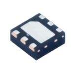
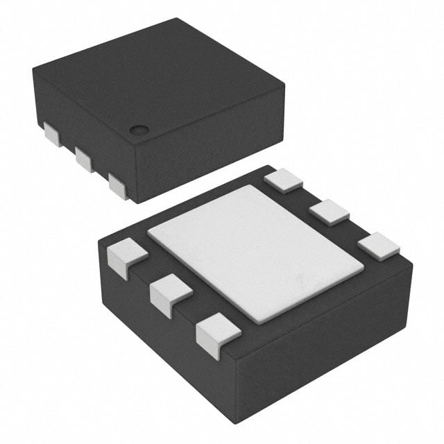
| 供应商器件封装 | 6-SON(2x2) |
| 其它名称 | 296-23998-6 |
| 内部开关 | 是 |
| 包装 | Digi-Reel® |
| 单位重量 | 9.700 mg |
| 商标 | Texas Instruments |
| 安装类型 | 表面贴装 |
| 安装风格 | SMD/SMT |
| 封装 | Reel |
| 封装/外壳 | 6-WDFN 裸露焊盘 |
| 封装/箱体 | WSON-6 |
| 工作温度 | -40°C ~ 85°C |
| 工作温度范围 | - 40 C to + 85 C |
| 工厂包装数量 | 250 |
| 开关数量 | Single |
| 开关类型 | 通用 |
| 最大工作温度 | + 85 C |
| 最小工作温度 | - 40 C |
| 标准包装 | 1 |
| 比率-输入:输出 | 1:1 |
| 特性 | 压摆率受控型 |
| 电压-负载 | 2.5 V ~ 6.5 V |
| 电压-输入 | 2.5 V ~ 6.5 V |
| 电流-输出(最大值) | 75mA |
| 电流限制 | 可调 |
| 电源电压-最大 | 6.5 V |
| 电源电压-最小 | 2.5 V |
| 类型 | USB 开关 |
| 系列 | TPS2552-1 |
| 输入类型 | 非反相 |
| 输出数 | 1 |
| 输出类型 | N 通道 |


- 商务部:美国ITC正式对集成电路等产品启动337调查
- 曝三星4nm工艺存在良率问题 高通将骁龙8 Gen1或转产台积电
- 太阳诱电将投资9.5亿元在常州建新厂生产MLCC 预计2023年完工
- 英特尔发布欧洲新工厂建设计划 深化IDM 2.0 战略
- 台积电先进制程称霸业界 有大客户加持明年业绩稳了
- 达到5530亿美元!SIA预计今年全球半导体销售额将创下新高
- 英特尔拟将自动驾驶子公司Mobileye上市 估值或超500亿美元
- 三星加码芯片和SET,合并消费电子和移动部门,撤换高东真等 CEO
- 三星电子宣布重大人事变动 还合并消费电子和移动部门
- 海关总署:前11个月进口集成电路产品价值2.52万亿元 增长14.8%


PDF Datasheet 数据手册内容提取
Product Sample & Technical Tools & Support & Reference Folder Buy Documents Software Community Design TPS2552,TPS2553,TPS2552-1,TPS2553-1 SLVS841F–NOVEMBER2008–REVISEDAUGUST2016 TPS255xx Precision Adjustable Current-Limited Power-Distribution Switches 1 Features 3 Description • Upto1.5-AMaximumLoadCurrent The TPS255x and TPS255x-1 power-distribution 1 switches are intended for applications where • ±6%Current-LimitAccuracyat1.7A(Typical) precision current limiting is required or heavy • MeetsUSBCurrent-LimitingRequirements capacitive loads and short circuits are encountered • BackwardsCompatibleWithTPS2550and and provide up to 1.5 A of continuous load current. TPS2551 These devices offer a programmable current-limit threshold between 75 mA and 1.7 A (typical) through • AdjustableCurrentLimit:75mAto1700mA an external resistor. Current-limit accuracy as tight as (Typical) ±6% can be achieved at the higher current-limit • Constant-Current(TPS255x)andLatch-Off settings. The power-switch rise and fall times are (TPS255x-1)Versions controlled to minimize current surges during turnon andturnoff. • FastOvercurrentResponse-2µs(Typical) • 85-mΩ High-SideMOSFET(DBVPackage) TPS255x devices limit the output current to a safe level by using a constant-current mode when the • ReverseInput-OutputVoltageProtection output load exceeds the current-limit threshold. • OperatingRange:2.5Vto6.5V TPS255x-1 devices provide circuit breaker • Built-InSoftStart functionality by latching off the power switch during • 15-kVESDProtectionperIEC61000-4-2(With overcurrent or reverse-voltage situations. An internal reverse-voltage comparator disables the power- ExternalCapacitance) switch when the output voltage is driven higher than • ULListed– FileNo.E169910andNEMKO the input to protect devices on the input side of the IEC60950-1-am1ed2.0 switch. The FAULT output asserts low during • SeetheTISwitchPortfolio overcurrentandreverse-voltageconditions. 2 Applications DeviceInformation(1) PARTNUMBER PACKAGE BODYSIZE(NOM) • USBPortsandHubs SOT-23(6) 2.90mmx1.60mm • DigitalTVs TPS2552 WSON(6) 2.00mmx2.00mm • Set-TopBoxes SOT-23(6) 2.90mmx1.60mm • VOIPPhones TPS2553 WSON(6) 2.00mmx2.00mm (1) For all available packages, see the orderable addendum at theendofthedatasheet. TypicalApplication TPS2552/53 5V USB 0.1mF USB Data USB Input IN OUT Port R FAULT 100 kW 120 mF ILIM FaultSignal FAULT RILIM USB requirement only* 20 kW Control Signal EN GND *USB requirement that downstream Power Pad facing ports are bypassed with at least 120 mF per hub Copyright © 2016,Texas Instruments Incorporated 1 An IMPORTANT NOTICE at the end of this data sheet addresses availability, warranty, changes, use in safety-critical applications, intellectualpropertymattersandotherimportantdisclaimers.PRODUCTIONDATA.
TPS2552,TPS2553,TPS2552-1,TPS2553-1 SLVS841F–NOVEMBER2008–REVISEDAUGUST2016 www.ti.com Table of Contents 1 Features.................................................................. 1 10 ApplicationandImplementation........................ 17 2 Applications........................................................... 1 10.1 ApplicationInformation..........................................17 3 Description............................................................. 1 10.2 TypicalApplications..............................................17 4 RevisionHistory..................................................... 2 11 PowerSupplyRecommendations..................... 24 5 DeviceComparisonTable..................................... 4 11.1 Self-PoweredandBus-PoweredHubs.................24 11.2 Low-PowerBus-PoweredandHigh-PowerBus- 6 PinConfigurationandFunctions......................... 5 PoweredFunctions..................................................24 7 Specifications......................................................... 5 11.3 PowerDissipationandJunctionTemperature......24 7.1 AbsoluteMaximumRatings......................................5 12 Layout................................................................... 25 7.2 ESDRatings ............................................................6 12.1 LayoutGuidelines.................................................25 7.3 RecommendedOperatingConditions.......................6 12.2 LayoutExample....................................................25 7.4 ThermalInformation..................................................6 13 DeviceandDocumentationSupport................. 26 7.5 ElectricalCharacteristics...........................................7 13.1 DeviceSupport......................................................26 7.6 TypicalCharacteristics..............................................8 13.2 RelatedLinks........................................................26 8 ParameterMeasurementInformation................11 13.3 ReceivingNotificationofDocumentationUpdates26 9 DetailedDescription............................................ 13 13.4 CommunityResources..........................................26 9.1 Overview.................................................................13 13.5 Trademarks...........................................................26 9.2 FunctionalBlockDiagram.......................................13 13.6 ElectrostaticDischargeCaution............................26 9.3 FeatureDescription.................................................13 13.7 Glossary................................................................26 9.4 DeviceFunctionalModes........................................15 14 Mechanical,Packaging,andOrderable 9.5 Programming...........................................................15 Information........................................................... 26 4 Revision History NOTE:Pagenumbersforpreviousrevisionsmaydifferfrompagenumbersinthecurrentversion. ChangesfromRevisionE(February2012)toRevisionF Page • AddedESDRatingtable,FeatureDescriptionsection,DeviceFunctionalModes,ApplicationandImplementation section,PowerSupplyRecommendationssection,Layoutsection,DeviceandDocumentationSupportsection,and Mechanical,Packaging,andOrderableInformationsection ................................................................................................. 1 • Changed1300mAto1700mAintheadjustablecurrentlimitbulletundertheFeaturessection......................................... 1 • Changedfrom1.2Ato1.5A.................................................................................................................................................. 4 ChangesfromRevisionD(June2011)toRevisionE Page • ChangedV toV inRecommendedOperatingConditions............................................................................................... 6 EN EN • ChangedV toV inRecommendedOperatingConditions............................................................................................... 6 EN EN ChangesfromRevisionC(September2009)toRevisionD Page • ChangedFrom:FastOvercurrentResponse-2-µS(typ)To:FastOvercurrentResponse-2-µs(typ)intheFeatures......1 • AddedtextToFeature-ULListed"andNEMKOIEC60950-1-am1ed2.0"........................................................................... 1 • AddedFeaturesItem"SeetheTISwitchPortfoilo"................................................................................................................ 1 • ChangedtheDEVICEINFORMATIONtable,andDeletedNote3........................................................................................ 1 • AddedESD-systemlevel(contact/air)totheABSMAXtable,andAddedNote3................................................................ 6 • AddedtexttotheREVERSE-VOLTAGEPROTECTIONsection:"Areverse.....whenthisoccurs.".................................... 14 2 SubmitDocumentationFeedback Copyright©2008–2016,TexasInstrumentsIncorporated ProductFolderLinks:TPS2552 TPS2553 TPS2552-1 TPS2553-1
TPS2552,TPS2553,TPS2552-1,TPS2553-1 www.ti.com SLVS841F–NOVEMBER2008–REVISEDAUGUST2016 ChangesfromRevisionB(February2009)toRevisionC Page • AddedFeature-Upto1.5AMaximumLoadCurrent............................................................................................................ 1 • Changed1.3A(typ)To:1.7A(typ)....................................................................................................................................... 1 • AddedText-andprovideupto1.5Aofcontinuousloadcurrent.......................................................................................... 1 • ChangedFrom:19.1kΩ≤R ≤232kΩTo:15kΩ≤R ≤232kΩ.................................................................................. 5 ILIM ILIM • ChangedI valuesfor1.2Aand1.5A................................................................................................................................. 6 OUT • ChangedT valuesfor1.2Aand1.5A.................................................................................................................................... 6 J • AddedR =15kΩoption.................................................................................................................................................... 7 ILIM • ChangedTextFrom:current-limitthresholdbetween75mAand1.3A(typ)To:current-limitthresholdbetween75 mAand1.7A(typ)................................................................................................................................................................ 13 • ChangedTextFrom:Therecommended1%resistorrangeforR is19.1kΩ≤R ≤232kΩtoensurestability ILIM ILIM To:Therecommended1%resistorrangeforR is15kΩ≤R ≤232kΩtoensurestability........................................ 15 ILIM ILIM • ChangedFrom:where19.1kΩ≤R ≤232kΩ.To:where15kΩ≤R ≤232kΩ......................................................... 15 ILIM ILIM • ChangedFigure23-Current-LimitThresholdvsR ........................................................................................................ 16 ILIM • ChangedTable2-addedrowsforCurrentLimitof1400to1700....................................................................................... 19 ChangesfromRevisionA(December2008)toRevisionB Page • AddedToFeatures-ULListed–FileNo.E169910.............................................................................................................. 1 • ChangedFigure17TtitleFrom:CurrentLimitThresholdVsR ......................................................................................... 9 ILM • ChangedFigure18TtitleFrom:CurrentLimitThresholdVsR ......................................................................................... 9 ILM ChangesfromOriginal(November2008)toRevisionA Page • ChangedTitlefrom:AdjustableCurrent-LimitedPower-DistributionSwitchesto:PrecisionAdjustableCurrent- LimitedPower-DistributionSwitches...................................................................................................................................... 1 Copyright©2008–2016,TexasInstrumentsIncorporated SubmitDocumentationFeedback 3 ProductFolderLinks:TPS2552 TPS2553 TPS2552-1 TPS2553-1
TPS2552,TPS2553,TPS2552-1,TPS2553-1 SLVS841F–NOVEMBER2008–REVISEDAUGUST2016 www.ti.com 5 Device Comparison Table 4 SubmitDocumentationFeedback Copyright©2008–2016,TexasInstrumentsIncorporated ProductFolderLinks:TPS2552 TPS2553 TPS2552-1 TPS2553-1
TPS2552,TPS2553,TPS2552-1,TPS2553-1 www.ti.com SLVS841F–NOVEMBER2008–REVISEDAUGUST2016 6 Pin Configuration and Functions TPS255xDBVPackage 6-PinSOT-23 TPS255xDRVPackage TopView 6-PinWSON TopView IN 1 6 OUT GND 2 5 ILIM OUT 1 6 IN EN 3 4 FAULT ILIM 2 PAD 5 GND FAULT 3 4 EN EN=ActiveLowfortheTPS2552 EN=ActiveLowfortheTPS2552 EN=ActiveHighfortheTPS2553 EN=ActiveHighfortheTPS2553 Add–1topartnumberforlatch-offversion Add–1topartnumberforlatch-offversion PinFunctions PIN TPS2552 TPS2553 I/O DESCRIPTION NAME SOT-23 WSON SOT-23 WSON EN 3 4 — — I Enableinput,logiclowturnsonpowerswitch EN — — 3 4 I Enableinput,logichighturnsonpowerswitch Active-lowopen-drainoutput,assertedduring FAULT 4 3 4 3 O overcurrent,overtemperature,orreverse-voltage conditions. GND 2 5 2 5 — Groundconnection;connectexternallytoPowerPAD Externalresistorusedtosetcurrent-limitthreshold; ILIM 5 2 5 2 O recommended15kΩ≤R ≤232kΩ. ILIM Inputvoltage;connecta0.1µForgreaterceramic IN 1 6 1 6 I capacitorfromINtoGNDasclosetotheICas possible. OUT 6 1 6 1 O Power-switchoutput InternallyconnectedtoGND;usedtoheat-sinkthepart PowerPAD™ — PAD — PAD — tothecircuitboardtraces.ConnectPowerPADtoGND pinexternally. Add–1forLatch-Offversion 7 Specifications 7.1 Absolute Maximum Ratings overoperatingfree-airtemperaturerange(unlessotherwisenoted) (1)(2) MIN MAX UNIT VoltagerangeonIN,OUT,ENorEN,ILIM,FAULT –0.3 7 V VoltagerangefromINtoOUT –7 7 V I Continuousoutputcurrent InternallyLimited O Continuoustotalpowerdissipation SeetheThermalInformation ContinuousFAULTsinkcurrent 0 25 mA ILIMsourcecurrent 0 1 mA T Maximumjunctiontemperature –40 150 °C J T Storagetemperature –65 150 °C stg (1) StressesbeyondthoselistedunderAbsoluteMaximumRatingsmaycausepermanentdamagetothedevice.Thesearestressratings only,whichdonotimplyfunctionaloperationofthedeviceattheseoranyotherconditionsbeyondthoseindicatedunderRecommended OperatingConditions.Exposuretoabsolute-maximum-ratedconditionsforextendedperiodsmayaffectdevicereliability. (2) VoltagesarereferencedtoGNDunlessotherwisenoted. Copyright©2008–2016,TexasInstrumentsIncorporated SubmitDocumentationFeedback 5 ProductFolderLinks:TPS2552 TPS2553 TPS2552-1 TPS2553-1
TPS2552,TPS2553,TPS2552-1,TPS2553-1 SLVS841F–NOVEMBER2008–REVISEDAUGUST2016 www.ti.com 7.2 ESD Ratings VALUE UNIT Humanbodymodel(HBM),perANSI/ESDA/JEDECJS-001(1) ±2000 Chargeddevicemodel(CDM),perJEDECspecificationJESD22- V Electrostaticdischarge C101(2) ±500 V (ESD) IEC61000-4-2contactdischarge(3) ±8000 IEC61000-4-2air-gapdischarge(3) ±15000 (1) JEDECdocumentJEP155statesthat500-VHBMallowssafemanufacturingwithastandardESDcontrolprocess. (2) JEDECdocumentJEP157statesthat250-VCDMallowssafemanufacturingwithastandardESDcontrolprocess. (3) SurgesperEN61000-4-2.1999appliedtooutputterminalsofEVM.Thesearepassingtestlevels,notfailurethreshold. 7.3 Recommended Operating Conditions overoperatingfree-airtemperaturerange(unlessotherwisenoted) MIN NOM MAX UNIT V Inputvoltage,IN 2.5 6.5 V IN V Enablevoltage TPS2552/52-1 0 6.5 V EN V Enablevoltage TPS2553/53-1 0 6.5 V EN V High-levelinputvoltageonENorEN 1.1 IH V V Low-levelinputvoltageonENorEN 0.66 IL Continuousoutputcurrent, –40°C≤TJ≤125°C 0 1.2 I A OUT OUT –40°C≤T ≤105°C 0 1.5 J R Current-limitthresholdresistorrange(nominal1%)fromILIMtoGND 15 232 kΩ ILIM I ContinuousFAULTsinkcurrent 0 10 mA O Inputde-couplingcapacitance,INtoGND 0.1 µF Operatingvirtualjunction IOUT≤1.2A –40 125 TJ temperature(1) I ≤1.5A –40 105 °C OUT (1) SeePowerDissipationandJunctionTemperaturefordetailsonhowtocalculatemaximumjunctiontemperatureforspecificapplications andpackages. 7.4 Thermal Information TPS2552 TPS2553 THERMALMETRIC(1) DBV(SOT-23) DRV(WSON) DBV(SOT-23) DRV(WSON) UNIT 6PINS 6PINS 6PINS 6PINS R Junction-to-ambientthermalresistance 182.6 72 182.6 72 °C/W θJA R θJC(to Junction-to-case(top)thermalresistance 122.2 85.3 122.2 85.3 °C/W p) R Junction-to-boardthermalresistance 29.4 41.3 29.4 41.3 °C/W θJB ψ Junction-to-topcharacterizationparameter 20.8 1.7 20.8 1.7 °C/W JT ψ Junction-to-boardcharacterizationparameter 28.9 41.7 28.9 41.7 °C/W JB R θJC(b Junction-to-case(bottom)thermalresistance — 11.1 — 11.1 °C/W ot) (1) Formoreinformationabouttraditionalandnewthermalmetrics,seetheSemiconductorandICPackageThermalMetricsapplication report. 6 SubmitDocumentationFeedback Copyright©2008–2016,TexasInstrumentsIncorporated ProductFolderLinks:TPS2552 TPS2553 TPS2552-1 TPS2553-1
TPS2552,TPS2553,TPS2552-1,TPS2553-1 www.ti.com SLVS841F–NOVEMBER2008–REVISEDAUGUST2016 7.5 Electrical Characteristics overrecommendedoperatingconditions,V =0V,orV =V ,R =10kΩ(unlessotherwisenoted) EN EN IN FAULT PARAMETER TESTCONDITIONS(1) MIN TYP MAX UNIT POWERSWITCH DBVpackage,TJ=25°C 85 95 DBVpackage,–40°C≤TJ≤125°C 135 rDS(on) Staticdrain-sourceon-stateresistance DRVpackage,TJ=25°C 100 115 mΩ DRVpackage,–40°C≤TJ≤105°C 140 DRVpackage,–40°C≤TJ≤125°C 150 tr Risetime,output C(sLe=eF1igµuFr,eR2L0=)100Ω, VVIINN==62..55VV 10..17 1.51 ms tf Falltime,output C(sLe=eF1igµuFr,eR2L0=)100Ω, VVIINN==62..55VV 00..22 00..55 ENABLEINPUTENOREN Enablepinturnon/offthreshold 0.66 1.1 V IEN Inputcurrent VEN=0Vor6.5V,VEN=0Vor6.5V –0.5 0.5 µA ton Turnontime CL=1µF,RL=100Ω,(seeFigure20) 3 ms toff Turnofftime CL=1µF,RL=100Ω,(seeFigure20) 3 ms CURRENTLIMIT RILIM=15kΩ,–40°C≤TJ≤105°C 1610 1700 1800 TJ=25°C 1215 1295 1375 RILIM=20kΩ Current-limitthreshold(MaximumDC –40°C≤TJ≤125°C 1200 1295 1375 IOS oacounntdpnuSethccoteurdtr-rcetionrctGuIOiNtUDcTudrreelnivte,rOedUTtoload) RILIM=49.9kΩ T–4J0=°C25≤°TCJ≤125°C 449705 552200 555605 mA RILIM=210kΩ 110 130 150 ILIMshortedtoIN 50 75 100 tIOS Responsetimetoshortcircuit VIN=5V(seeFigure21) 2 µs REVERSE-VOLTAGEPROTECTION Reverse-voltagecomparatortrippoint 95 135 190 mV (VOUT–VIN) Timefromreverse-voltagecondition toMOSFETturnoff VIN=5V 3 5 7 ms SUPPLYCURRENT IIN_off Supplycurrent,low-leveloutput VIN=6.5V,NoloadonOUT,VEN=6.5VorVEN=0V 0.1 1 µA RILIM=20kΩ 120 140 µA IIN_on Supplycurrent,high-leveloutput VIN=6.5V,NoloadonOUT RILIM=210kΩ 100 120 µA IREV Reverseleakagecurrent VOUT=6.5V,VIN=0V TJ=25°C 0.01 1 µA UNDERVOLTAGELOCKOUT UVLO Low-levelinputvoltage,IN VINrising 2.35 2.45 V Hysteresis,IN TJ=25°C 25 mV FAULTFLAG VOL Outputlowvoltage,FAULT I/FAULT=1mA 180 mV Off-stateleakage V/FAULT=6.5V 1 µA FAULTassertionorde-assertionduetoovercurrentcondition 5 7.5 10 ms FAULTdeglitch FAULTassertionorde-assertionduetoreverse-voltagecondition 2 4 6 ms THERMALSHUTDOWN Thermalshutdownthreshold 155 °C Thermalshutdownthresholdin 135 °C current-limit Hysteresis 10 °C (1) Pulse-testingtechniquesmaintainjunctiontemperatureclosetoambienttemperature;thermaleffectsmustbetakenintoaccount separately. Copyright©2008–2016,TexasInstrumentsIncorporated SubmitDocumentationFeedback 7 ProductFolderLinks:TPS2552 TPS2553 TPS2552-1 TPS2553-1
TPS2552,TPS2553,TPS2552-1,TPS2553-1 SLVS841F–NOVEMBER2008–REVISEDAUGUST2016 www.ti.com 7.6 Typical Characteristics Figure1.TurnonDelayandRiseTime Figure2.TurnoffDelayandFallTime Figure3.DeviceEnabledintoShort-Circuit Figure4.Full-LoadtoShort-CircuitTransientResponse Figure5.Short-CircuittoFull-LoadRecoveryResponse Figure6.No-LoadtoShort-CircuitTransientResponse 8 SubmitDocumentationFeedback Copyright©2008–2016,TexasInstrumentsIncorporated ProductFolderLinks:TPS2552 TPS2553 TPS2552-1 TPS2553-1
TPS2552,TPS2553,TPS2552-1,TPS2553-1 www.ti.com SLVS841F–NOVEMBER2008–REVISEDAUGUST2016 Typical Characteristics (continued) Figure7.Short-CircuittoNo-LoadRecoveryResponse Figure8.NoLoadto1-ΩTransientResponse Figure10.Reverse-VoltageProtectionResponse Figure9.1-ΩtoNoLoadTransientResponse 2.40 2.39 RILIM= 20 kW O - Undervoltage Lockout - V222222......333333345678 UVLO RUisVinLgO Falling UVL2.32 2.31 2.30 -50 0 50 100 150 TJ- Junction Temperature - °C Figure11.Reverse-VoltageProtectionRecovery Figure12.UVLO–UndervoltageLockout–V Copyright©2008–2016,TexasInstrumentsIncorporated SubmitDocumentationFeedback 9 ProductFolderLinks:TPS2552 TPS2553 TPS2552-1 TPS2553-1
TPS2552,TPS2553,TPS2552-1,TPS2553-1 SLVS841F–NOVEMBER2008–REVISEDAUGUST2016 www.ti.com Typical Characteristics (continued) 0.40 150 Current, Output Disabled -Am 000000......122233604826 RILIM= 20 kW VIN= 6.5 V Current, Output Enabled -Am 111023679505050 RILIM= 20 kW VIN= 6.V5 IVN= 2.5V IVN= 5 VVIN= 3.3 V I- Supply IN000...001482 VIN= 2.5 V I- Supply IN 134505 0 0 -50 0 50 100 150 -50 0 50 100 150 TJ- Junction Temperature - °C TJ- Junction Temperature - °C Figure13.I –SupplyCurrent,OutputDisabled–µA Figure14.I –SupplyCurrent,OutputEnabled–µA IN IN 20 150 Current Limit Response -sm 11111024682468 VRTAIINLI=M= 2 5=5 °V2C,0 kW, Wr- Static Drain-Source On-State Resistance - mDS(on)1125702505050 DRV Package DBV Package -50 0 50 100 150 00 1.5 3 4.5 6 TJ- Junction Temperature - °C Peak Current -A Figure15.CurrentLimitResponse–µs Figure16.MOSFETr Vs.JunctionTemperature DS(on) 1400 150 1300 140 1200 130 IDS - Static Drain-Source Current - mA11123456789010000000000000000000000 TTATAA== 1= -2 42505°°°CCC VRIINLIM= 6=. 52 0V ,kW IDS - Static Drain-Source Current - mA 111123456789012000000000000 TA= -40°C TA= 25°C TA= 125°CVRIINLIM= 6=. 52 0V0, kW 0 0 100 200 300 400 500 600 700 800 900 1000 0 VIN- VOUT- 100 mV/div 0 100 200 300 VIN40-0 VOUT50- 0100 m6V0/0div 700 800 900 1000 Figure17.SwitchCurrentVs.Drain-SourceVoltageAcross Figure18.SwitchCurrentVs.Drain-SourceVoltageAcross Switch Switch 10 SubmitDocumentationFeedback Copyright©2008–2016,TexasInstrumentsIncorporated ProductFolderLinks:TPS2552 TPS2553 TPS2552-1 TPS2553-1
TPS2552,TPS2553,TPS2552-1,TPS2553-1 www.ti.com SLVS841F–NOVEMBER2008–REVISEDAUGUST2016 8 Parameter Measurement Information TPS2552 VIN 10mF VOUT IN OUT R FAULT 10 kW 150mF ILIM FaultSignal FAULT R ILIM Control Signal EN GND Power Pad Figure19. TypicalCharacteristicsReferenceSchematic OUT t t r f RL CL V 90% 90% OUT 10% 10% TEST CIRCUIT VEN 50% 50% VEN 50% 50% toff ton toff t t on off 90% 90% VOUT 10% VOUT 10% VOLTAGE WAVEFORMS Figure20. TestCircuitandVoltageWaveforms I OS I OUT t IOS Figure21. ResponseTimetoShort-CircuitWaveform Copyright©2008–2016,TexasInstrumentsIncorporated SubmitDocumentationFeedback 11 ProductFolderLinks:TPS2552 TPS2553 TPS2552-1 TPS2553-1
TPS2552,TPS2553,TPS2552-1,TPS2553-1 SLVS841F–NOVEMBER2008–REVISEDAUGUST2016 www.ti.com Parameter Measurement Information (continued) Decreasing Load Resistance V OUT Decreasing Load Resistance I OUT I OS Figure22. OutputVoltagevsCurrent-LimitThreshold 12 SubmitDocumentationFeedback Copyright©2008–2016,TexasInstrumentsIncorporated ProductFolderLinks:TPS2552 TPS2553 TPS2552-1 TPS2553-1
TPS2552,TPS2553,TPS2552-1,TPS2553-1 www.ti.com SLVS841F–NOVEMBER2008–REVISEDAUGUST2016 9 Detailed Description 9.1 Overview The TPS255x and TPS255x-1 are current-limited, power-distribution switches using N-channel MOSFETs for applications where short circuits or heavy capacitive loads are encountered and provide up to 1.5 A of continuous load current. These devices allow the user to program the current-limit threshold between 75 mA and 1.7 A (typical) through an external resistor. Additional device shutdown features include overtemperature protection and reverse-voltage protection. The device incorporates an internal charge pump and gate drive circuitry necessary to drive the N-channel MOSFET. The charge pump supplies power to the driver circuit and provides the necessary voltage to pull the gate of the MOSFET above the source. The charge pump operates from input voltages as low as 2.5 V and requires little supply current. The driver controls the gate voltage of the power switch. The driver incorporates circuitry that controls the rise and fall times of the output voltage to limit large current and voltage surges and provides built-in soft-start functionality. There are two device families that handle overcurrent situations differently. The TPS255x family enters constant-current mode while the TPS255x-1 familylatchesoffwhentheloadexceedsthecurrent-limitthreshold. 9.2 Functional Block Diagram - Reverse Voltage + Comparator IN CS OUT Current h Sense 4-mseglitc Charge D Pump Current EN Driver Limit FAULT (NoteA) UVLO GND Thermal Sense 8-ms Deglitch ILIM Copyright © 2016,Texas Instruments Incorporated A. TPS255xpartsenterconstantcurrentmodeduringcurrentlimitcondition;TPS255x-1partslatchoff 9.3 Feature Description 9.3.1 OvercurrentConditions The TPS255x and TPS255x-1 respond to overcurrent conditions by limiting their output current to the I levels OS shown in Figure 23. When an overcurrent condition is detected, the device maintains a constant output current andreducestheoutputvoltageaccordingly.Twopossibleoverloadconditionscanoccur. The first condition is when a short circuit or partial short circuit is present when the device is powered-up or enabled. The output voltage is held near zero potential with respect to ground and the TPS255x ramps the output current to I . The TPS255x devices limits the current to I until the overload condition is removed or the OS OS device begins to thermal cycle. The TPS255x-1 devices will limit the current to I until the overload condition is OS removed or the internal deglitch time (7.5-ms typical) is reached and the device is turned off. The device remains offuntilpoweriscycledorthedeviceenableistoggled. Copyright©2008–2016,TexasInstrumentsIncorporated SubmitDocumentationFeedback 13 ProductFolderLinks:TPS2552 TPS2553 TPS2552-1 TPS2553-1
TPS2552,TPS2553,TPS2552-1,TPS2553-1 SLVS841F–NOVEMBER2008–REVISEDAUGUST2016 www.ti.com Feature Description (continued) The second condition is when a short circuit, partial short circuit, or transient overload occurs while the device is enabled and powered on. The device responds to the overcurrent condition within time t (see Figure 21). The IOS current-sense amplifier is overdriven during this time and momentarily disables the internal current-limit MOSFET. The current-sense amplifier recovers and limits the output current to I . Similar to the previous case, OS the TPS255x limits the current to I until the overload condition is removed or the device begins to thermal OS cycle; the TPS255x-1 limits the current to I until the overload condition is removed or the internal deglitch time OS isreachedandthedeviceislatchedoff. The TPS255x thermal cycles if an overload condition is present long enough to activate thermal limiting in any of the above cases. The device turns off when the junction temperature exceeds 135°C (typical) while in current limit. The device remains off until the junction temperature cools 10°C (typical) and then restarts. The TPS255x cyclesonandoffuntiltheoverloadisremoved(seeFigure5andFigure7). 9.3.2 Reverse-VoltageProtection The reverse-voltage protection feature turns off the N-channel MOSFET whenever the output voltage exceeds theinputvoltageby135mV(typical)for4-ms(typical). Areversecurrentof(V –V )/r )arepresentwhen OUT IN DS(on) this occurs. This prevents damage to devices on the input side of the TPS255x and TPS2552-1/TPS2253-1 by preventing significant current from sinking into the input capacitance. The TPS255x devices allow the N-channel MOSFET to turn on once the output voltage goes below the input voltage for the same 4-ms deglitch time. The TPS255x-1 devices keep the device turned off even if the reverse-voltage condition is removed and do not allow the N-channel MOSFET to turn on until power is cycled or the device enable is toggled. The reverse-voltage comparatoralsoassertstheFAULToutput(active-low)after4-ms. 9.3.3 FAULTResponse TheFAULTopen-drainoutputisasserted(activelow)duringanovercurrent,overtemperature,orreverse-voltage condition. The TPS255x asserts the FAULT signal until the fault condition is removed and the device resumes normal operation. The TPS255x-1 asserts the FAULT signal during a fault condition and remains asserted while thepartislatched-off.The FAULTsignalisde-assertedoncedevicepoweriscycledortheenableistoggledand the device resumes normal operation. The TPS255x and TPS255x-1 are designed to eliminate false FAULT reporting by using an internal delay de-glitch circuit for overcurrent (7.5-ms typical) and reverse-voltage (4-ms typical) conditions without the need for external circuitry. This ensures that FAULT is not accidentally asserted due to normal operation such as starting into a heavy capacitive load. The deglitch circuitry delays entering and leavingfaultconditions.Overtemperatureconditionsarenotdeglitchedandassertthe FAULTsignalimmediately. 9.3.4 UndervoltageLockout(UVLO) The undervoltage lockout (UVLO) circuit disables the power switch until the input voltage reaches the UVLO turnon threshold. Built-in hysteresis prevents unwanted on and off cycling due to input voltage drop from large currentsurges. 9.3.5 ENABLE(ENorEN) The logic enable controls the power switch, bias for the charge pump, driver, and other circuits to reduce the supply current. The supply current is reduced to less than 1-µA when a logic low is present on EN. A logic low input on EN or a logic high input on EN enables the driver, control circuits, and power switch. The enable input is compatiblewithbothTTLandCMOSlogiclevels. 9.3.6 ThermalSense The TPS255x and TPS255x-1 have self-protection features using two independent thermal-sensing circuits that monitor the operating temperature of the power switch and disable operation if the temperature exceeds recommended operating conditions. The TPS255x device operates in constant-current mode during an overcurrent conditions, which increases the voltage drop across power-switch. The power dissipation in the package is proportional to the voltage drop across the power switch, which increases the junction temperature during an overcurrent condition. The first thermal sensor turns off the power switch when the die temperature exceeds 135°C (minimum) and the part is in current limit. Hysteresis is built into the thermal sensor, and the switchturnsonafterthedevicehascooledapproximately10°C. 14 SubmitDocumentationFeedback Copyright©2008–2016,TexasInstrumentsIncorporated ProductFolderLinks:TPS2552 TPS2553 TPS2552-1 TPS2553-1
TPS2552,TPS2553,TPS2552-1,TPS2553-1 www.ti.com SLVS841F–NOVEMBER2008–REVISEDAUGUST2016 Feature Description (continued) The TPS255x and TPS255x-1 also have a second ambient thermal sensor. The ambient thermal sensor turns off the power-switch when the die temperature exceeds 155°C (minimum) regardless of whether the power switch is in current limit and turns on the power switch after the device has cooled approximately 10°C. The TPS255x and TPS255x-1familiescontinue tocycleoffandonuntilthefaultisremoved. The open-drain fault reporting output FAULT is asserted (active low) immediately during an overtemperature shutdowncondition. 9.4 Device Functional Modes Therearenootherfunctionalmodes. 9.5 Programming 9.5.1 ProgrammingtheCurrent-LimitThreshold The overcurrent threshold is user programmable through an external resistor. The TPS255x and TPS255x-1 use an internal regulation loop to provide a regulated voltage on the ILIM pin. The current-limit threshold is proportional to the current sourced out of ILIM. The recommended 1% resistor range for R is 15 kΩ ≤ R ≤ ILIM ILIM 232 kΩ to ensure stability of the internal regulation loop. Many applications require that the minimum current limit is above a certain current level or that the maximum current limit is below a certain current level, so it is important to consider the tolerance of the overcurrent threshold when selecting a value for R . The following ILIM equations and Figure 23 can be used to calculate the resulting overcurrent threshold for a given external resistor value (R ). Figure 23 includes current-limit tolerance due to variations caused by temperature and process. ILIM However, the equations do not account for tolerance due to external resistor variation, so it is important to account for this tolerance when selecting R . The traces routing the R resistor to the TPS255x and ILIM ILIM TPS255x-1 mustbeasshortaspossibletoreduceparasiticeffectsonthecurrent-limitaccuracy. R can be selected to provide a current-limit threshold that occurs 1) above a minimum load current or 2) ILIM belowamaximumloadcurrent. To design above a minimum current-limit threshold, find the intersection of R and the maximum desired load ILIM current on the I curve and choose a value of R below this value. Programming the current limit above a OS(min) ILIM minimum threshold is important to ensure start-up into full load or heavy capacitive loads. The resulting maximumcurrent-limitthresholdistheintersectionoftheselectedvalueofR andtheI curve. ILIM OS(max) To design below a maximum current-limit threshold, find the intersection of R and the maximum desired load ILIM current on the I curve and choose a value of R above this value. Programming the current limit below a OS(max) ILIM maximum threshold is important to avoid current limiting upstream power supplies, causing the input voltage bus to droop. The resulting minimum current-limit threshold is the intersection of the selected value of R and the ILIM I curve. OS(min) Current-LimitThresholdEquations(I ): OS I (mA)= 22980V OSmax R 0.94kW ILIM I (mA)= 23950V OSnom R 0.977kW ILIM I (mA)= 25230V OSmin R 1.016kW ILIM where 15kΩ≤ R ≤ 232kΩ. (1) ILIM While the maximum recommended value of RILIM is 232 kΩ, there is one additional configuration that allows for a lower current-limit threshold. The ILIM pin may be connected directly to IN to provide a 75 mA (typical) current- limit threshold. Additional low-ESR ceramic capacitance may be necessary from IN to GND in this configuration topreventunwantednoisefromcouplingintothesensitiveILIMcircuitry. Copyright©2008–2016,TexasInstrumentsIncorporated SubmitDocumentationFeedback 15 ProductFolderLinks:TPS2552 TPS2553 TPS2552-1 TPS2553-1
TPS2552,TPS2553,TPS2552-1,TPS2553-1 SLVS841F–NOVEMBER2008–REVISEDAUGUST2016 www.ti.com Programming (continued) 1800 1700 1600 1500 A 1400 m d - 1300 ol 1200 h s 1100 e hr 1000 T mit 900 IOS(max) Li 800 nt 700 e urr 600 C 500 IOS(nom) 400 300 200 IOS(min) 100 0 15 25 35 45 55 65 75 85 95 105115125135145 155165175185195205215225235 R - Current Limit Resistor - kW ILIM Figure23. Current-LimitThresholdvsR ILIM 16 SubmitDocumentationFeedback Copyright©2008–2016,TexasInstrumentsIncorporated ProductFolderLinks:TPS2552 TPS2553 TPS2552-1 TPS2553-1
TPS2552,TPS2553,TPS2552-1,TPS2553-1 www.ti.com SLVS841F–NOVEMBER2008–REVISEDAUGUST2016 10 Application and Implementation NOTE Information in the following applications sections is not part of the TI component specification, and TI does not warrant its accuracy or completeness. TI’s customers are responsible for determining suitability of components for their purposes. Customers should validateandtesttheirdesignimplementationtoconfirmsystemfunctionality. 10.1 Application Information 10.1.1 Constant-CurrentvsLatch-OffOperationandImpactonOutputVoltage Boththeconstant-currentdevices(TPS255x)andlatch-offdevices(TPS255x-1)operateidenticallyduringnormal operation, that is, the load current is less than the current-limit threshold and the devices are not limiting current. During normal operation the N-channel MOSFET is fully enhanced, and V = V - (I x r ). The voltage OUT IN OUT DS(on) dropacrosstheMOSFETisrelativelysmallcomparedtoV ,andV ≉V . IN OUT IN Both the constant-current devices (TPS255x ) and latch-off devices (TPS255x-1) operate identically during the initial onset of an overcurrent event. Both devices limit current to the programmed current-limit threshold set to R by operating the N-channel MOSFET in the linear mode. During current-limit operation, the N-channel ILIM MOSFET is no longer fully-enhanced and the resistance of the device increases. This allows the device to effectively regulate the current to the current-limit threshold. The effect of increasing the resistance of the MOSFETisthatthevoltagedropacrossthedeviceisnolongernegligible(V ≠V ),andV decreases.The IN OUT OUT amount that V decreases is proportional to the magnitude of the overload condition. The expected V can OUT OUT becalculatedby, I ×R OS LOAD where I isthecurrent-limitthresholdandR isthemagnitudeoftheoverloadcondition. (2) OS LOAD Forexample,ifI isprogrammedto1Aanda1Ω overloadconditionisapplied,theresultingV is1V. OS OUT While both the constant-current devices (TPS255x ) and latch-off devices (TPS255x-1) operate identically during the initial onset of an overcurrent event, they behave differently if the overcurrent event lasts longer than the internal delay de-glitch circuit (7.5-ms typical). The constant-current devices (TPS255x ) assert the FAULT flag after the deglitch period and continue to regulate the current to the current-limit threshold indefinitely. In practical circuits, the power dissipation in the package increases the die temperature above the overtemperature shutdown threshold (135°C minimum), and the device turns off until the die temperature decreases by the hysteresisofthethermalshutdowncircuit(10°Ctypical).Thedeviceturnsonandcontinuestothermalcycleuntil the overload condition is removed. The constant-current devices resume normal operation once the overload condition is removed. The latch-off devices (TPS255x-1) assert the FAULT flag after the deglitch period and immediately turn off the device. The device remains off regardless of whether the overload condition is removed from the output. The latch-off devices remain off and do not resume normal operation until the surrounding systemeithertogglestheenableorcyclespowertothedevice. 10.2 Typical Applications 10.2.1 Two-LevelCurrent-LimitCircuit Some applications require different current-limit thresholds depending on external system conditions. Figure 24 shows an implementation for an externally controlled, two-level current-limit circuit. The current-limit threshold is set by the total resistance from ILIM to GND (see the Programming the Current-Limit Threshold section). A logic- level input enables or disables MOSFET Q1 and changes the current-limit threshold by modifying the total resistance from ILIM to GND. Additional MOSFET and resistor combinations can be used in parallel to Q1/R2 to increasethenumberofadditionalcurrent-limitlevels. NOTE ILIMmustneverbedrivendirectlywithanexternalsignal. Copyright©2008–2016,TexasInstrumentsIncorporated SubmitDocumentationFeedback 17 ProductFolderLinks:TPS2552 TPS2553 TPS2552-1 TPS2553-1
TPS2552,TPS2553,TPS2552-1,TPS2553-1 SLVS841F–NOVEMBER2008–REVISEDAUGUST2016 www.ti.com Typical Applications (continued) Input 0.1mF Output IN OUT RFAULT CLOAD RLOAD 100 kW R1 210 kW ILIM FaultSignal FAULT R2 22.1 kW Control Signal EN GND Power Pad Q1 Current Limit 2N7002 Control Signal Copyright © 2016,Texas Instruments Incorporated Figure24. Two-LevelCurrent-LimitCircuit 10.2.1.1 DesignRequirements Forthisexample,usetheparametersshowninTable1. Table1.DesignRequirements PARAMETER VALUE Inputvoltage 5V Outputvoltage 5V Aboveaminimumcurrentlimit 1000mA Belowamaximumcurrentlimit 500mA 10.2.1.2 DetailedDesignProcedures 10.2.1.2.1 DesigningAboveaMinimumCurrentLimit Some applications require that current limiting cannot occur below a certain threshold. For this example, assume that 1 A must be delivered to the load so that the minimum desired current-limit threshold is 1000 mA. Use the I equationsandFigure23toselectR . OS ILIM I (mA)=1000mA OSmin I (mA)= 25230V OSmin RILIM1.016kW 1 RILIM(kW)= æççççèIO2S5m2i3nm0VAö÷÷÷÷ø1.016 RILIM(kW)=24kW (3) Select the closest 1% resistor less than the calculated value: R = 23.7 kΩ. This sets the minimum current-limit ILIM threshold at 1 A . Use the I equations, Figure 23, and the previously calculated value for R to calculate the OS ILIM maximumresultingcurrent-limitthreshold. R (kW)=23.7kW ILIM 22980V I (mA)= OSmax R 0.94kW ILIM 22980V I (mA)= OSmax 23.70.94kW I (mA)=1172.4mA OSmax (4) Theresultingmaximumcurrent-limitthresholdis1172.4mAwitha23.7-kΩresistor. 18 SubmitDocumentationFeedback Copyright©2008–2016,TexasInstrumentsIncorporated ProductFolderLinks:TPS2552 TPS2553 TPS2552-1 TPS2553-1
TPS2552,TPS2553,TPS2552-1,TPS2553-1 www.ti.com SLVS841F–NOVEMBER2008–REVISEDAUGUST2016 10.2.1.2.2 DesigningBelowaMaximumCurrentLimit Some applications require that current limiting must occur below a certain threshold. For this example, assume that the desired upper current-limit threshold must be below 500 mA to protect an up-stream power supply. Use theI equationsandFigure23toselectR . OS ILIM I (mA)=500mA OSmax I (mA)= 22980V OSmax R 0.94kW ILIM 1 RILIM(kW)= æççççèI22980mVAö÷÷÷÷ø0.94 OSmax R (kW)=58.7kW ILIM (5) Select the closest 1% resistor greater than the calculated value: R = 59-kΩ. This sets the maximum current- ILIM limit threshold at 500 mA . Use the I equations, Figure 23, and the previously calculated value for R to OS ILIM calculatetheminimumresultingcurrent-limitthreshold. R (kW)=59kW ILIM 25230V I (mA)= OSmin R 1.016kW ILIM 25230V I (mA)= OSmin 591.016kW I (mA)=400.6mA OSmin (6) Theresultingminimumcurrent-limitthresholdis400.6mAwitha59-kΩresistor. 10.2.1.2.3 AccountingforResistorTolerance The previous sections described the selection of R given certain application requirements and the importance ILIM of understanding the current-limit threshold tolerance. The analysis focused only on the TPS255x and TPS255x- 1 performance and assumed an exact resistor value. However, resistors sold in quantity are not exact and are bounded by an upper and lower tolerance centered around a nominal resistance. The additional R resistance ILIM tolerance directly affects the current-limit threshold accuracy at a system level. The following table shows a process that accounts for worst-case resistor tolerance assuming 1% resistor values. Step one follows the selection process outlined in the application examples above. Step two determines the upper and lower resistance bounds of the selected resistor. Step three uses the upper and lower resistor bounds in the I OS equations to calculate the threshold limits. It is important to use tighter tolerance resistors, for example, 0.5% or 0.1%,whenprecisioncurrentlimitingisdesired. Copyright©2008–2016,TexasInstrumentsIncorporated SubmitDocumentationFeedback 19 ProductFolderLinks:TPS2552 TPS2553 TPS2552-1 TPS2553-1
TPS2552,TPS2553,TPS2552-1,TPS2553-1 SLVS841F–NOVEMBER2008–REVISEDAUGUST2016 www.ti.com Table2.CommonR ResistorSelections ILIM DESIRED RESISTORTOLERANCE ACTUALLIMITS NOMINAL IDEAL CLOSEST CURRENT RESISTOR 1%RESISTOR 1%HIGHT LIMIT (kΩ) (kΩ) 1%LOW(kΩ) (kΩ) IOSMIN(mA) IOSNOM(mA) IOSMAX(mA) (mA) 75 SHORTILIMtoIN 50.0 75.0 100.0 120 226.1 226 223.7 228.3 101.3 120.0 142.1 200 134.0 133 131.7 134.3 173.7 201.5 233.9 300 88.5 88.7 87.8 89.6 262.1 299.4 342.3 400 65.9 66.5 65.8 67.2 351.2 396.7 448.7 500 52.5 52.3 51.8 52.8 448.3 501.6 562.4 600 43.5 43.2 42.8 43.6 544.3 604.6 673.1 700 37.2 37.4 37.0 37.8 630.2 696.0 770.8 800 32.4 32.4 32.1 32.7 729.1 800.8 882.1 900 28.7 28.7 28.4 29.0 824.7 901.5 988.7 1000 25.8 26.1 25.8 26.4 908.3 989.1 1081.0 1100 23.4 23.2 23.0 23.4 1023.7 1109.7 1207.5 1200 21.4 21.5 21.3 21.7 1106.0 1195.4 1297.1 1300 19.7 19.6 19.4 19.8 1215.1 1308.5 1414.9 1400 18.3 18.2 18.0 18.4 1310.1 1406.7 1517.0 1500 17.0 16.9 16.7 17.1 1412.5 1512.4 1626.4 1600 16.0 15.8 15.6 16.0 1512.5 1615.2 1732.7 1700 15.0 15.0 14.9 15.2 1594.5 1699.3 1819.4 10.2.1.2.4 InputandOutputCapacitance Input and output capacitance improves the performance of the device; the actual capacitance must be optimized for the particular application. For all applications, TI recommends placing a 0.1-µF or greater ceramic bypass capacitor between IN and GND as close to the device as possible for local noise de-coupling. This precaution reduces ringing on the input due to power-supply transients. Additional input capacitance may be needed on the input to reduce voltage overshoot from exceeding the absolute maximum voltage of the device during heavy transient conditions. This is especially important during bench testing when long, inductive cables are used to connecttheevaluationboardtothebenchpower-supply. TI recommends placing a high-value electrolytic capacitor on the output pin when large transient currents are expectedontheoutput. 10.2.1.3 ApplicationCurves Figure25.TurnonDelayandRiseTime Figure26.Reverse-VoltageProtectionRecovery 20 SubmitDocumentationFeedback Copyright©2008–2016,TexasInstrumentsIncorporated ProductFolderLinks:TPS2552 TPS2553 TPS2552-1 TPS2553-1
TPS2552,TPS2553,TPS2552-1,TPS2553-1 www.ti.com SLVS841F–NOVEMBER2008–REVISEDAUGUST2016 10.2.2 Auto-RetryFunctionality Some applications require that an overcurrent condition disables the part momentarily during a fault condition andre-enablesafterapre-settime.Thisauto-retryfunctionalitycanbeimplementedwithanexternalresistorand capacitor. During a fault condition, FAULT pulls low disabling the part. The part is disabled when EN is pulled low, and FAULT goes high impedance allowing C to begin charging. The part re-enables when the voltage RETRY on EN reaches the turnon threshold, and the auto-retry time is determined by the resistor-capacitor time constant.Thedevicecontinuestocycleinthismanneruntilthefaultconditionisremoved. TPS2553 Input 0.1mF Output IN OUT RFAULT RLOAD C 100 kW LOAD ILIM R FAULT ILIM 20 kW EN GND C RETRY 0.1mF Power Pad Copyright © 2016,Texas Instruments Incorporated Figure27. Auto-RetryFunctionality Someapplicationsrequireauto-retryfunctionalityandtheabilitytoenableordisablewithanexternallogicsignal. Figure 28 shows how an external logic signal can drive EN through R and maintain auto-retry functionality. FAULT Theresistor-capacitortimeconstantdeterminestheauto-retrytime-outperiod. TPS2553 0.1mF Input Output IN OUT R LOAD C LOAD External Logic ILIM Signal &Driver RFAULT FAULT RILIM 100 kW 20 kW EN GND C RETRY 0.1mF Power Pad Copyright © 2016,Texas Instruments Incorporated Figure28. Auto-RetryFunctionalityWithExternalENSignal 10.2.2.1 DesignRequirements Forthisexample,usetheparametersshowninTable3. Table3.DesignRequirements PARAMETER VALUE Inputvoltage 5V Outputvoltage 5V Current 1200mA Copyright©2008–2016,TexasInstrumentsIncorporated SubmitDocumentationFeedback 21 ProductFolderLinks:TPS2552 TPS2553 TPS2552-1 TPS2553-1
TPS2552,TPS2553,TPS2552-1,TPS2553-1 SLVS841F–NOVEMBER2008–REVISEDAUGUST2016 www.ti.com 10.2.2.2 DetailedDesignProcedure RefertoProgrammingtheCurrent-LimitThresholdsectionforthecurrentlimitsetting.Forauto-retryfunctionality, once FAULT asserted, EN pull low, TPS2553 is disabled, FAULT des-asserted, C is slowly charged to EN RETRY logic high through R , then enable, after deglitch time, FAULT asserted again. In the event of an overload, FAULT TPS2553cyclesandhasoutputaveragecurrent.ON-timewithoutputcurrentisdecidedby FAULTdeglitchtime. OFF-time without output current is decided by R x C constant time to EN logic high and t time. FAULT RETRY on Therefore,settheR ×C togetthedesiredoutputaveragecurrentduringoverload. FAULT RETRY 10.2.3 TypicalApplicationasUSBPowerSwitch TPS2552/53 5V USB 0.1mF USB Data USB Input IN OUT Port R FAULT 100 kW 120mF ILIM FaultSignal FAULT RILIM 20 kW USB requirement only* Control Signal EN GND *USB requirement that downstream Power Pad facing ports are bypassed with at least 120mF per hub Copyright © 2016,Texas Instruments Incorporated Figure29. TypicalApplicationasUSBPowerSwitch 10.2.3.1 DesignRequirements Forthisexample,usetheparametersshowninTable4. Table4.DesignRequirements PARAMETER VALUE Inputvoltage 5V Outputvoltage 5V Current 1200mA 10.2.3.1.1 USBPower-DistributionRequirements USB can be implemented in several ways regardless of the type of USB device being developed. Several power- distributionfeaturesmustbeimplemented. • SPHsmust: – Currentlimitdownstreamports – Reportovercurrentconditions • BPHsmust: – Enableordisablepowertodownstreamports – Powerupat <100mA – Limitinrushcurrent(<44 Ωand10µF) • Functionsmust: – Limitinrushcurrents – Powerupat <100mA The feature set of the TPS255x and TPS255x-1 meets each of these requirements. The integrated current limiting and overcurrent reporting is required by self-powered hubs. The logic-level enable and controlled rise times meet the need of both input and output ports on bus-powered hubs and the input ports for bus-powered functions. 22 SubmitDocumentationFeedback Copyright©2008–2016,TexasInstrumentsIncorporated ProductFolderLinks:TPS2552 TPS2553 TPS2552-1 TPS2553-1
TPS2552,TPS2553,TPS2552-1,TPS2553-1 www.ti.com SLVS841F–NOVEMBER2008–REVISEDAUGUST2016 10.2.3.2 DetailedDesignProcedure 10.2.3.2.1 UniversalSerialBus(USB)Power-DistributionRequirements One application for this device is for current limiting in universal serial bus (USB) applications. The original USB interface was a 12-Mbps or 1.5-Mbps, multiplexed serial bus designed for low-to-medium bandwidth PC peripherals (for example, keyboards, printers, scanners, and mice). As the demand for more bandwidth increased, the USB 2.0 standard was introduced increasing the maximum data rate to 480-Mbps. The four-wire USBinterfaceisconceivedfordynamicattach-detach(hotplug-unplug)ofperipherals.Twolinesareprovidedfor differentialdata,andtwolinesareprovidedfor5-Vpowerdistribution. USB data is a 3.3-V level signal, but power is distributed at 5 V to allow for voltage drops in cases where power is distributed through more than one hub across long cables. Each function must provide its own regulated 3.3 V from the 5-V input or its own internal power supply. The USB specification classifies two different classes of devices depending on its maximum current draw. A device classified as low-power can draw up to 100 mA as defined by the standard. A device classified as high-power can draw up to 500 mA. It is important that the minimum current-limit threshold of the current-limiting power-switch exceed the maximum current-limit draw of the intended application. The latest USB standard must always be referenced when considering the current-limit threshold The USB specification defines two types of devices as hubs and functions. A USB hub is a device that contains multiple ports for different USB devices to connect and can be self-powered (SPH) or bus-powered (BPH). A function is a USB device that is able to transmit or receive data or control information over the bus. A USB functioncanbeembeddedinaUSBhub.AUSBfunctioncanbeoneofthreetypesincludedinthelistbelow. • Low-power,bus-poweredfunction • High-power,bus-poweredfunction • Self-poweredfunction SPHs and BPHs distribute data and power to downstream functions. The TPS255x has higher current capability thanrequiredforasingleUSBportallowingittopowermultipledownstreamports. Copyright©2008–2016,TexasInstrumentsIncorporated SubmitDocumentationFeedback 23 ProductFolderLinks:TPS2552 TPS2553 TPS2552-1 TPS2553-1
TPS2552,TPS2553,TPS2552-1,TPS2553-1 SLVS841F–NOVEMBER2008–REVISEDAUGUST2016 www.ti.com 11 Power Supply Recommendations 11.1 Self-Powered and Bus-Powered Hubs A SPH has a local power supply that powers embedded functions and downstream ports. This power supply must provide between 4.75 V to 5.25 V to downstream facing devices under full-load and no-load conditions. SPHs are required to have current-limit protection and must report overcurrent conditions to the USB controller. TypicalSPHsaredesktopPCs,monitors,printers,andstand-alonehubs. A BPH obtains all power from an upstream port and often contains an embedded function. It must power up with less than 100 mA. The BPH usually has one embedded function, and power is always available to the controller of the hub. If the embedded function and hub require more than 100 mA on power up, keep the power to the embedded function off until enumeration is completed. This can be accomplished by removing power or by shutting off the clock to the embedded function. Power-switching the embedded function is not necessary if the aggregate power draw for the function and controller is less than 100 mA. The total current drawn by the bus- powered device is the sum of the current to the controller, the embedded function, and the downstream ports, anditislimitedto500mAfromanupstreamport. 11.2 Low-Power Bus-Powered and High-Power Bus-Powered Functions Both low-power and high-power bus-powered functions obtain all power from upstream ports. Low-power functionsalwaysdrawlessthan100mA;high-powerfunctionsmustdrawlessthan100mAatpowerupandcan draw up to 500 mA after enumeration. If the load of the function is more than the parallel combination of 44 Ω and10µFatpowerup,thedevicemustimplementinrushcurrentlimiting. 11.3 Power Dissipation and Junction Temperature The low ON-resistance of the N-channel MOSFET allows small surface-mount packages to pass large currents. It is good design practice to estimate power dissipation and junction temperature. The below analysis gives an approximation for calculating junction temperature based on the power dissipation in the package. However, it is important to note that thermal analysis is strongly dependent on additional system level factors. Such factors include air flow, board layout, copper thickness and surface area, and proximity to other devices dissipating power. Good thermal design practice must include all system level factors in addition to individual component analysis. Begin by determining the r of the N-channel MOSFET relative to the input voltage and operating DS(on) temperature. As an initial estimate, use the highest operating ambient temperature of interest and read r DS(on) fromthetypicalcharacteristicsgraph.Usingthisvalue,thepowerdissipationcanbecalculatedusingEquation7. P =r ×I 2 D DS(on) OUT where • P =Totalpowerdissipation(W) D • r =Powerswitchon-resistance(Ω) DS(on) • I =Maximumcurrent-limitthreshold(A) OUT • ThisstepcalculatesthetotalpowerdissipationoftheN-channelMOSFET. (7) Finally,calculatethejunctiontemperature: T =P ×θ +T J D JA A where • T =Ambienttemperature(°C) A • θ =Thermalresistance(°C/W) JA • P =Totalpowerdissipation(W) (8) D Compare the calculated junction temperature with the initial estimate. If they are not within a few degrees, repeat the calculation using the refined r from the previous calculation as the new estimate. Two or three iterations DS(on) are generally sufficient to achieve the desired result. The final junction temperature is highly dependent on thermal resistance θ , and thermal resistance is highly dependent on the individual package and board layout. JA TheThermalInformationtableprovidesexamplethermalresistancesforspecificpackagesandboardlayouts. 24 SubmitDocumentationFeedback Copyright©2008–2016,TexasInstrumentsIncorporated ProductFolderLinks:TPS2552 TPS2553 TPS2552-1 TPS2553-1
TPS2552,TPS2553,TPS2552-1,TPS2553-1 www.ti.com SLVS841F–NOVEMBER2008–REVISEDAUGUST2016 12 Layout 12.1 Layout Guidelines • TI recommends placing the 100-nF bypass capacitor near the IN and GND pins, and make the connections usingalow-inductancetrace. • TI recommends placing a high-value electrolytic capacitor and a 100-nF bypass capacitor on the output pin whenlargetransientcurrentsareexpectedontheoutput. • The traces routing the RILIM resistor to the device must be as short as possible to reduce parasitic effects on thecurrentlimitaccuracy. • ThePowerPADmustbedirectlyconnectedtoPCBgroundplaneusingwideandshortcoppertrace. 12.2 Layout Example /FAULT IN 1 6 OUT 2 5 ILIM EN 3 4 Figure30. LayoutRecommendation Copyright©2008–2016,TexasInstrumentsIncorporated SubmitDocumentationFeedback 25 ProductFolderLinks:TPS2552 TPS2553 TPS2552-1 TPS2553-1
TPS2552,TPS2553,TPS2552-1,TPS2553-1 SLVS841F–NOVEMBER2008–REVISEDAUGUST2016 www.ti.com 13 Device and Documentation Support 13.1 Device Support FortheTISwitchPortfolio,gohere. 13.2 Related Links The table below lists quick access links. Categories include technical documents, support and community resources,toolsandsoftware,andquickaccesstosampleorbuy. Table5.RelatedLinks TECHNICAL TOOLS& SUPPORT& PARTS PRODUCTFOLDER SAMPLE&BUY DOCUMENTS SOFTWARE COMMUNITY TPS32552 Clickhere Clickhere Clickhere Clickhere Clickhere TPS2553 Clickhere Clickhere Clickhere Clickhere Clickhere TPS2552-1 Clickhere Clickhere Clickhere Clickhere Clickhere TPS2553-1 Clickhere Clickhere Clickhere Clickhere Clickhere 13.3 Receiving Notification of Documentation Updates To receive notification of documentation updates, navigate to the device product folder on ti.com. In the upper right corner, click on Alert me to register and receive a weekly digest of any product information that has changed.Forchangedetails,reviewtherevisionhistoryincludedinanyreviseddocument. 13.4 Community Resources The following links connect to TI community resources. Linked contents are provided "AS IS" by the respective contributors. They do not constitute TI specifications and do not necessarily reflect TI's views; see TI's Terms of Use. TIE2E™OnlineCommunity TI'sEngineer-to-Engineer(E2E)Community.Createdtofostercollaboration amongengineers.Ate2e.ti.com,youcanaskquestions,shareknowledge,exploreideasandhelp solveproblemswithfellowengineers. DesignSupport TI'sDesignSupport QuicklyfindhelpfulE2Eforumsalongwithdesignsupporttoolsand contactinformationfortechnicalsupport. 13.5 Trademarks PowerPAD,E2EaretrademarksofTexasInstruments. Allothertrademarksarethepropertyoftheirrespectiveowners. 13.6 Electrostatic Discharge Caution Thesedeviceshavelimitedbuilt-inESDprotection.Theleadsshouldbeshortedtogetherorthedeviceplacedinconductivefoam duringstorageorhandlingtopreventelectrostaticdamagetotheMOSgates. 13.7 Glossary SLYZ022—TIGlossary. Thisglossarylistsandexplainsterms,acronyms,anddefinitions. 14 Mechanical, Packaging, and Orderable Information The following pages include mechanical, packaging, and orderable information. This information is the most current data available for the designated devices. This data is subject to change without notice and revision of thisdocument.Forbrowser-basedversionsofthisdatasheet,refertotheleft-handnavigation. 26 SubmitDocumentationFeedback Copyright©2008–2016,TexasInstrumentsIncorporated ProductFolderLinks:TPS2552 TPS2553 TPS2552-1 TPS2553-1
PACKAGE OPTION ADDENDUM www.ti.com 6-Feb-2020 PACKAGING INFORMATION Orderable Device Status Package Type Package Pins Package Eco Plan Lead/Ball Finish MSL Peak Temp Op Temp (°C) Device Marking Samples (1) Drawing Qty (2) (6) (3) (4/5) HPA00615DRVR ACTIVE WSON DRV 6 3000 Green (RoHS NIPDAU Level-1-260C-UNLIM -40 to 85 CHT & no Sb/Br) HPA00714DBVR ACTIVE SOT-23 DBV 6 3000 Green (RoHS NIPDAU Level-1-260C-UNLIM -40 to 85 2552 & no Sb/Br) TPS2552DBVR ACTIVE SOT-23 DBV 6 3000 Green (RoHS NIPDAU Level-1-260C-UNLIM -40 to 85 2552 & no Sb/Br) TPS2552DBVR-1 ACTIVE SOT-23 DBV 6 3000 Green (RoHS NIPDAU Level-1-260C-UNLIM -40 to 85 CHX & no Sb/Br) TPS2552DBVT ACTIVE SOT-23 DBV 6 250 Green (RoHS NIPDAU Level-1-260C-UNLIM -40 to 85 2552 & no Sb/Br) TPS2552DBVT-1 ACTIVE SOT-23 DBV 6 250 Green (RoHS NIPDAU Level-1-260C-UNLIM -40 to 85 CHX & no Sb/Br) TPS2552DRVR ACTIVE WSON DRV 6 3000 Green (RoHS NIPDAU Level-1-260C-UNLIM -40 to 85 CHR & no Sb/Br) TPS2552DRVR-1 ACTIVE WSON DRV 6 3000 Green (RoHS NIPDAU Level-1-260C-UNLIM -40 to 85 CHY & no Sb/Br) TPS2552DRVT ACTIVE WSON DRV 6 250 Green (RoHS NIPDAU Level-1-260C-UNLIM -40 to 85 CHR & no Sb/Br) TPS2552DRVT-1 ACTIVE WSON DRV 6 250 Green (RoHS NIPDAU Level-1-260C-UNLIM -40 to 85 CHY & no Sb/Br) TPS2553DBVR ACTIVE SOT-23 DBV 6 3000 Green (RoHS NIPDAU Level-1-260C-UNLIM -40 to 85 2553 & no Sb/Br) TPS2553DBVR-1 ACTIVE SOT-23 DBV 6 3000 Green (RoHS NIPDAU Level-1-260C-UNLIM -40 to 85 CHZ & no Sb/Br) TPS2553DBVT ACTIVE SOT-23 DBV 6 250 Green (RoHS NIPDAU Level-1-260C-UNLIM -40 to 85 2553 & no Sb/Br) TPS2553DBVT-1 ACTIVE SOT-23 DBV 6 250 Green (RoHS NIPDAU Level-1-260C-UNLIM -40 to 85 CHZ & no Sb/Br) TPS2553DRVR ACTIVE WSON DRV 6 3000 Green (RoHS NIPDAU Level-1-260C-UNLIM -40 to 85 CHT & no Sb/Br) TPS2553DRVR-1 ACTIVE WSON DRV 6 3000 Green (RoHS NIPDAU Level-1-260C-UNLIM -40 to 85 CJZ & no Sb/Br) TPS2553DRVT ACTIVE WSON DRV 6 250 Green (RoHS NIPDAU Level-1-260C-UNLIM -40 to 85 CHT & no Sb/Br) Addendum-Page 1
PACKAGE OPTION ADDENDUM www.ti.com 6-Feb-2020 Orderable Device Status Package Type Package Pins Package Eco Plan Lead/Ball Finish MSL Peak Temp Op Temp (°C) Device Marking Samples (1) Drawing Qty (2) (6) (3) (4/5) TPS2553DRVT-1 ACTIVE WSON DRV 6 250 Green (RoHS NIPDAU Level-1-260C-UNLIM -40 to 85 CJZ & no Sb/Br) (1) The marketing status values are defined as follows: ACTIVE: Product device recommended for new designs. LIFEBUY: TI has announced that the device will be discontinued, and a lifetime-buy period is in effect. NRND: Not recommended for new designs. Device is in production to support existing customers, but TI does not recommend using this part in a new design. PREVIEW: Device has been announced but is not in production. Samples may or may not be available. OBSOLETE: TI has discontinued the production of the device. (2) RoHS: TI defines "RoHS" to mean semiconductor products that are compliant with the current EU RoHS requirements for all 10 RoHS substances, including the requirement that RoHS substance do not exceed 0.1% by weight in homogeneous materials. Where designed to be soldered at high temperatures, "RoHS" products are suitable for use in specified lead-free processes. TI may reference these types of products as "Pb-Free". RoHS Exempt: TI defines "RoHS Exempt" to mean products that contain lead but are compliant with EU RoHS pursuant to a specific EU RoHS exemption. Green: TI defines "Green" to mean the content of Chlorine (Cl) and Bromine (Br) based flame retardants meet JS709B low halogen requirements of <=1000ppm threshold. Antimony trioxide based flame retardants must also meet the <=1000ppm threshold requirement. (3) MSL, Peak Temp. - The Moisture Sensitivity Level rating according to the JEDEC industry standard classifications, and peak solder temperature. (4) There may be additional marking, which relates to the logo, the lot trace code information, or the environmental category on the device. (5) Multiple Device Markings will be inside parentheses. Only one Device Marking contained in parentheses and separated by a "~" will appear on a device. If a line is indented then it is a continuation of the previous line and the two combined represent the entire Device Marking for that device. (6) Lead/Ball Finish - Orderable Devices may have multiple material finish options. Finish options are separated by a vertical ruled line. Lead/Ball Finish values may wrap to two lines if the finish value exceeds the maximum column width. Important Information and Disclaimer:The information provided on this page represents TI's knowledge and belief as of the date that it is provided. TI bases its knowledge and belief on information provided by third parties, and makes no representation or warranty as to the accuracy of such information. Efforts are underway to better integrate information from third parties. TI has taken and continues to take reasonable steps to provide representative and accurate information but may not have conducted destructive testing or chemical analysis on incoming materials and chemicals. TI and TI suppliers consider certain information to be proprietary, and thus CAS numbers and other limited information may not be available for release. In no event shall TI's liability arising out of such information exceed the total purchase price of the TI part(s) at issue in this document sold by TI to Customer on an annual basis. OTHER QUALIFIED VERSIONS OF TPS2553, TPS2553-1 : •Automotive: TPS2553-Q1, TPS2553-Q1 Addendum-Page 2
PACKAGE OPTION ADDENDUM www.ti.com 6-Feb-2020 NOTE: Qualified Version Definitions: •Automotive - Q100 devices qualified for high-reliability automotive applications targeting zero defects Addendum-Page 3
PACKAGE MATERIALS INFORMATION www.ti.com 30-Apr-2020 TAPE AND REEL INFORMATION *Alldimensionsarenominal Device Package Package Pins SPQ Reel Reel A0 B0 K0 P1 W Pin1 Type Drawing Diameter Width (mm) (mm) (mm) (mm) (mm) Quadrant (mm) W1(mm) TPS2552DBVR SOT-23 DBV 6 3000 180.0 8.4 3.2 3.2 1.4 4.0 8.0 Q3 TPS2552DBVR SOT-23 DBV 6 3000 179.0 8.4 3.2 3.2 1.4 4.0 8.0 Q3 TPS2552DBVR SOT-23 DBV 6 3000 178.0 9.0 3.23 3.17 1.37 4.0 8.0 Q3 TPS2552DBVR-1 SOT-23 DBV 6 3000 178.0 9.0 3.23 3.17 1.37 4.0 8.0 Q3 TPS2552DBVR-1 SOT-23 DBV 6 3000 179.0 8.4 3.2 3.2 1.4 4.0 8.0 Q3 TPS2552DBVT SOT-23 DBV 6 250 178.0 9.0 3.23 3.17 1.37 4.0 8.0 Q3 TPS2552DBVT SOT-23 DBV 6 250 179.0 8.4 3.2 3.2 1.4 4.0 8.0 Q3 TPS2552DBVT SOT-23 DBV 6 250 180.0 8.4 3.2 3.2 1.4 4.0 8.0 Q3 TPS2552DBVT-1 SOT-23 DBV 6 250 179.0 8.4 3.2 3.2 1.4 4.0 8.0 Q3 TPS2552DBVT-1 SOT-23 DBV 6 250 178.0 9.0 3.23 3.17 1.37 4.0 8.0 Q3 TPS2552DRVR WSON DRV 6 3000 180.0 8.4 2.3 2.3 1.15 4.0 8.0 Q2 TPS2552DRVR-1 WSON DRV 6 3000 179.0 8.4 2.2 2.2 1.2 4.0 8.0 Q2 TPS2552DRVT WSON DRV 6 250 180.0 8.4 2.3 2.3 1.15 4.0 8.0 Q2 TPS2552DRVT-1 WSON DRV 6 250 179.0 8.4 2.2 2.2 1.2 4.0 8.0 Q2 TPS2553DBVR SOT-23 DBV 6 3000 178.0 9.0 3.23 3.17 1.37 4.0 8.0 Q3 TPS2553DBVR SOT-23 DBV 6 3000 179.0 8.4 3.2 3.2 1.4 4.0 8.0 Q3 TPS2553DBVR-1 SOT-23 DBV 6 3000 178.0 9.0 3.23 3.17 1.37 4.0 8.0 Q3 TPS2553DBVR-1 SOT-23 DBV 6 3000 179.0 8.4 3.2 3.2 1.4 4.0 8.0 Q3 PackMaterials-Page1
PACKAGE MATERIALS INFORMATION www.ti.com 30-Apr-2020 Device Package Package Pins SPQ Reel Reel A0 B0 K0 P1 W Pin1 Type Drawing Diameter Width (mm) (mm) (mm) (mm) (mm) Quadrant (mm) W1(mm) TPS2553DBVR-1 SOT-23 DBV 6 3000 180.0 8.4 3.2 3.2 1.4 4.0 8.0 Q3 TPS2553DBVT SOT-23 DBV 6 250 180.0 8.4 3.2 3.2 1.4 4.0 8.0 Q3 TPS2553DBVT SOT-23 DBV 6 250 179.0 8.4 3.2 3.2 1.4 4.0 8.0 Q3 TPS2553DBVT SOT-23 DBV 6 250 178.0 9.0 3.23 3.17 1.37 4.0 8.0 Q3 TPS2553DBVT-1 SOT-23 DBV 6 250 180.0 8.4 3.2 3.2 1.4 4.0 8.0 Q3 TPS2553DBVT-1 SOT-23 DBV 6 250 178.0 9.0 3.23 3.17 1.37 4.0 8.0 Q3 TPS2553DBVT-1 SOT-23 DBV 6 250 179.0 8.4 3.2 3.2 1.4 4.0 8.0 Q3 TPS2553DRVR WSON DRV 6 3000 180.0 8.4 2.3 2.3 1.15 4.0 8.0 Q2 TPS2553DRVR WSON DRV 6 3000 179.0 8.4 2.2 2.2 1.2 4.0 8.0 Q2 TPS2553DRVR-1 WSON DRV 6 3000 180.0 8.4 2.3 2.3 1.15 4.0 8.0 Q2 TPS2553DRVT WSON DRV 6 250 180.0 8.4 2.3 2.3 1.15 4.0 8.0 Q2 TPS2553DRVT-1 WSON DRV 6 250 180.0 8.4 2.3 2.3 1.15 4.0 8.0 Q2 *Alldimensionsarenominal Device PackageType PackageDrawing Pins SPQ Length(mm) Width(mm) Height(mm) TPS2552DBVR SOT-23 DBV 6 3000 210.0 185.0 35.0 TPS2552DBVR SOT-23 DBV 6 3000 203.0 203.0 35.0 TPS2552DBVR SOT-23 DBV 6 3000 180.0 180.0 18.0 TPS2552DBVR-1 SOT-23 DBV 6 3000 180.0 180.0 18.0 TPS2552DBVR-1 SOT-23 DBV 6 3000 203.0 203.0 35.0 PackMaterials-Page2
PACKAGE MATERIALS INFORMATION www.ti.com 30-Apr-2020 Device PackageType PackageDrawing Pins SPQ Length(mm) Width(mm) Height(mm) TPS2552DBVT SOT-23 DBV 6 250 180.0 180.0 18.0 TPS2552DBVT SOT-23 DBV 6 250 203.0 203.0 35.0 TPS2552DBVT SOT-23 DBV 6 250 210.0 185.0 35.0 TPS2552DBVT-1 SOT-23 DBV 6 250 203.0 203.0 35.0 TPS2552DBVT-1 SOT-23 DBV 6 250 180.0 180.0 18.0 TPS2552DRVR WSON DRV 6 3000 210.0 185.0 35.0 TPS2552DRVR-1 WSON DRV 6 3000 203.0 203.0 35.0 TPS2552DRVT WSON DRV 6 250 210.0 185.0 35.0 TPS2552DRVT-1 WSON DRV 6 250 203.0 203.0 35.0 TPS2553DBVR SOT-23 DBV 6 3000 180.0 180.0 18.0 TPS2553DBVR SOT-23 DBV 6 3000 203.0 203.0 35.0 TPS2553DBVR-1 SOT-23 DBV 6 3000 180.0 180.0 18.0 TPS2553DBVR-1 SOT-23 DBV 6 3000 203.0 203.0 35.0 TPS2553DBVR-1 SOT-23 DBV 6 3000 210.0 185.0 35.0 TPS2553DBVT SOT-23 DBV 6 250 210.0 185.0 35.0 TPS2553DBVT SOT-23 DBV 6 250 203.0 203.0 35.0 TPS2553DBVT SOT-23 DBV 6 250 180.0 180.0 18.0 TPS2553DBVT-1 SOT-23 DBV 6 250 210.0 185.0 35.0 TPS2553DBVT-1 SOT-23 DBV 6 250 180.0 180.0 18.0 TPS2553DBVT-1 SOT-23 DBV 6 250 203.0 203.0 35.0 TPS2553DRVR WSON DRV 6 3000 182.0 182.0 20.0 TPS2553DRVR WSON DRV 6 3000 203.0 203.0 35.0 TPS2553DRVR-1 WSON DRV 6 3000 210.0 185.0 35.0 TPS2553DRVT WSON DRV 6 250 182.0 182.0 20.0 TPS2553DRVT-1 WSON DRV 6 250 210.0 185.0 35.0 PackMaterials-Page3
GENERIC PACKAGE VIEW DRV 6 WSON - 0.8 mm max height PLASTIC SMALL OUTLINE - NO LEAD Images above are just a representation of the package family, actual package may vary. Refer to the product data sheet for package details. 4206925/F
PACKAGE OUTLINE DRV0006A WSON - 0.8 mm max height SCALE 5.500 PLASTIC SMALL OUTLINE - NO LEAD B 2.1 A 1.9 PIN 1 INDEX AREA 2.1 1.9 0.8 C 0.7 SEATING PLANE 0.08 C (0.2) TYP 1 0.1 0.05 EXPOSED 0.00 THERMAL PAD 3 4 2X 7 1.3 1.6 0.1 6 1 4X 0.65 0.35 6X PIN 1 ID 0.3 0.25 6X (OPTIONAL) 0.2 0.1 C A B 0.05 C 4222173/B 04/2018 NOTES: 1. All linear dimensions are in millimeters. Any dimensions in parenthesis are for reference only. Dimensioning and tolerancing per ASME Y14.5M. 2. This drawing is subject to change without notice. 3. The package thermal pad must be soldered to the printed circuit board for thermal and mechanical performance. www.ti.com
EXAMPLE BOARD LAYOUT DRV0006A WSON - 0.8 mm max height PLASTIC SMALL OUTLINE - NO LEAD 6X (0.45) (1) 1 7 6X (0.3) 6 SYMM (1.6) (1.1) 4X (0.65) 4 3 (R0.05) TYP SYMM ( 0.2) VIA (1.95) TYP LAND PATTERN EXAMPLE SCALE:25X 0.07 MAX 0.07 MIN ALL AROUND ALL AROUND SOLDER MASK METAL METAL UNDER SOLDER MASK OPENING SOLDER MASK OPENING NON SOLDER MASK DEFINED SOLDER MASK (PREFERRED) DEFINED SOLDER MASK DETAILS 4222173/B 04/2018 NOTES: (continued) 4. This package is designed to be soldered to a thermal pad on the board. For more information, see Texas Instruments literature number SLUA271 (www.ti.com/lit/slua271). 5. Vias are optional depending on application, refer to device data sheet. If some or all are implemented, recommended via locations are shown. www.ti.com
EXAMPLE STENCIL DESIGN DRV0006A WSON - 0.8 mm max height PLASTIC SMALL OUTLINE - NO LEAD SYMM 6X (0.45) METAL 1 7 6X (0.3) 6 (0.45) SYMM 4X (0.65) (0.7) 4 3 (R0.05) TYP (1) (1.95) SOLDER PASTE EXAMPLE BASED ON 0.125 mm THICK STENCIL EXPOSED PAD #7 88% PRINTED SOLDER COVERAGE BY AREA UNDER PACKAGE SCALE:30X 4222173/B 04/2018 NOTES: (continued) 6. Laser cutting apertures with trapezoidal walls and rounded corners may offer better paste release. IPC-7525 may have alternate design recommendations. www.ti.com
PACKAGE OUTLINE DRV0006D WSON - 0.8 mm max height SCALE 5.500 PLASTIC SMALL OUTLINE - NO LEAD B 2.1 A 1.9 PIN 1 INDEX AREA 2.1 1.9 0.8 C 0.7 SEATING PLANE 0.08 C (0.2) TYP 1 0.1 0.05 EXPOSED 0.00 THERMAL PAD 3 4 2X 7 1.3 1.6 0.1 6 1 4X 0.65 0.35 6X PIN 1 ID 0.3 0.25 6X (OPTIONAL) 0.2 0.1 C A B 0.05 C 4225563/A 12/2019 NOTES: 1. All linear dimensions are in millimeters. Any dimensions in parenthesis are for reference only. Dimensioning and tolerancing per ASME Y14.5M. 2. This drawing is subject to change without notice. 3. The package thermal pad must be soldered to the printed circuit board for thermal and mechanical performance. www.ti.com
EXAMPLE BOARD LAYOUT DRV0006D WSON - 0.8 mm max height PLASTIC SMALL OUTLINE - NO LEAD 6X (0.45) (1) 1 7 6X (0.3) 6 SYMM (1.6) (1.1) 4X (0.65) 4 3 (R0.05) TYP SYMM ( 0.2) VIA (1.95) TYP LAND PATTERN EXAMPLE EXPOSED METAL SHOWN SCALE:25X 0.07 MAX 0.07 MIN ALL AROUND ALL AROUND EXPOSED EXPOSED METAL METAL SOLDER MASK METAL METAL UNDER SOLDER MASK OPENING SOLDER MASK OPENING NON SOLDER MASK DEFINED SOLDER MASK (PREFERRED) DEFINED SOLDER MASK DETAILS 4225563/A 12/2019 NOTES: (continued) 4. This package is designed to be soldered to a thermal pad on the board. For more information, see Texas Instruments literature number SLUA271 (www.ti.com/lit/slua271). 5. Vias are optional depending on application, refer to device data sheet. If some or all are implemented, recommended via locations are shown. www.ti.com
EXAMPLE STENCIL DESIGN DRV0006D WSON - 0.8 mm max height PLASTIC SMALL OUTLINE - NO LEAD SYMM 6X (0.45) METAL 1 7 6X (0.3) 6 (0.45) SYMM 4X (0.65) (0.7) 4 3 (R0.05) TYP (1) (1.95) SOLDER PASTE EXAMPLE BASED ON 0.125 mm THICK STENCIL EXPOSED PAD #7 88% PRINTED SOLDER COVERAGE BY AREA UNDER PACKAGE SCALE:30X 4225563/A 12/2019 NOTES: (continued) 6. Laser cutting apertures with trapezoidal walls and rounded corners may offer better paste release. IPC-7525 may have alternate design recommendations. www.ti.com
PACKAGE OUTLINE DBV0006A SOT-23 - 1.45 mm max height SCALE 4.000 SMALL OUTLINE TRANSISTOR C 3.0 2.6 0.1 C 1.75 1.45 B A 1.45 MAX PIN 1 INDEX AREA 1 6 2X 0.95 3.05 2.75 1.9 5 2 4 3 0.50 6X 0.25 0.15 0.2 C A B (1.1) TYP 0.00 0.25 GAGE PLANE 0.22 TYP 0.08 8 TYP 0.6 0 0.3 TYP SEATING PLANE 4214840/B 03/2018 NOTES: 1. All linear dimensions are in millimeters. Any dimensions in parenthesis are for reference only. Dimensioning and tolerancing per ASME Y14.5M. 2. This drawing is subject to change without notice. 3. Body dimensions do not include mold flash or protrusion. Mold flash and protrusion shall not exceed 0.15 per side. 4. Leads 1,2,3 may be wider than leads 4,5,6 for package orientation. 5. Refernce JEDEC MO-178. www.ti.com
EXAMPLE BOARD LAYOUT DBV0006A SOT-23 - 1.45 mm max height SMALL OUTLINE TRANSISTOR PKG 6X (1.1) 1 6X (0.6) 6 SYMM 2 5 2X (0.95) 3 4 (R0.05) TYP (2.6) LAND PATTERN EXAMPLE EXPOSED METAL SHOWN SCALE:15X SOLDER MASK SOLDER MASK METAL UNDER METAL OPENING OPENING SOLDER MASK EXPOSED METAL EXPOSED METAL 0.07 MAX 0.07 MIN ARROUND ARROUND NON SOLDER MASK SOLDER MASK DEFINED DEFINED (PREFERRED) SOLDER MASK DETAILS 4214840/B 03/2018 NOTES: (continued) 6. Publication IPC-7351 may have alternate designs. 7. Solder mask tolerances between and around signal pads can vary based on board fabrication site. www.ti.com
EXAMPLE STENCIL DESIGN DBV0006A SOT-23 - 1.45 mm max height SMALL OUTLINE TRANSISTOR PKG 6X (1.1) 1 6X (0.6) 6 SYMM 2 5 2X(0.95) 3 4 (R0.05) TYP (2.6) SOLDER PASTE EXAMPLE BASED ON 0.125 mm THICK STENCIL SCALE:15X 4214840/B 03/2018 NOTES: (continued) 8. Laser cutting apertures with trapezoidal walls and rounded corners may offer better paste release. IPC-7525 may have alternate design recommendations. 9. Board assembly site may have different recommendations for stencil design. www.ti.com
IMPORTANTNOTICEANDDISCLAIMER TI PROVIDES TECHNICAL AND RELIABILITY DATA (INCLUDING DATASHEETS), DESIGN RESOURCES (INCLUDING REFERENCE DESIGNS), APPLICATION OR OTHER DESIGN ADVICE, WEB TOOLS, SAFETY INFORMATION, AND OTHER RESOURCES “AS IS” AND WITH ALL FAULTS, AND DISCLAIMS ALL WARRANTIES, EXPRESS AND IMPLIED, INCLUDING WITHOUT LIMITATION ANY IMPLIED WARRANTIES OF MERCHANTABILITY, FITNESS FOR A PARTICULAR PURPOSE OR NON-INFRINGEMENT OF THIRD PARTY INTELLECTUAL PROPERTY RIGHTS. These resources are intended for skilled developers designing with TI products. You are solely responsible for (1) selecting the appropriate TI products for your application, (2) designing, validating and testing your application, and (3) ensuring your application meets applicable standards, and any other safety, security, or other requirements. These resources are subject to change without notice. TI grants you permission to use these resources only for development of an application that uses the TI products described in the resource. Other reproduction and display of these resources is prohibited. No license is granted to any other TI intellectual property right or to any third party intellectual property right. TI disclaims responsibility for, and you will fully indemnify TI and its representatives against, any claims, damages, costs, losses, and liabilities arising out of your use of these resources. TI’s products are provided subject to TI’s Terms of Sale (www.ti.com/legal/termsofsale.html) or other applicable terms available either on ti.com or provided in conjunction with such TI products. TI’s provision of these resources does not expand or otherwise alter TI’s applicable warranties or warranty disclaimers for TI products. Mailing Address: Texas Instruments, Post Office Box 655303, Dallas, Texas 75265 Copyright © 2020, Texas Instruments Incorporated