ICGOO在线商城 > 集成电路(IC) > PMIC - 配电开关,负载驱动器 > VND5160JTR-E
 Datasheet下载
- 型号: VND5160JTR-E
- 制造商: STMicroelectronics
- 库位|库存: xxxx|xxxx
- 要求:
| 数量阶梯 | 香港交货 | 国内含税 |
| +xxxx | $xxxx | ¥xxxx |
查看当月历史价格
查看今年历史价格
VND5160JTR-E产品简介:
ICGOO电子元器件商城为您提供VND5160JTR-E由STMicroelectronics设计生产,在icgoo商城现货销售,并且可以通过原厂、代理商等渠道进行代购。 VND5160JTR-E价格参考。STMicroelectronicsVND5160JTR-E封装/规格:PMIC - 配电开关,负载驱动器, 。您可以下载VND5160JTR-E参考资料、Datasheet数据手册功能说明书,资料中有VND5160JTR-E 详细功能的应用电路图电压和使用方法及教程。
STMicroelectronics的VND5160JTR-E是一款PMIC(电源管理集成电路)中的配电开关/负载驱动器,适用于多种电子设备和系统中对功率控制和负载管理有需求的应用场景。以下是其主要应用场景:

 1. 消费类电子产品
   - 便携式设备:如智能手机、平板电脑、可穿戴设备等,用于管理电池供电下的负载切换,确保高效能耗。
   - 家用电器:例如智能家电中的电机控制或传感器驱动,提供稳定的电流输出以支持设备运行。

 2. 工业自动化
   - 传感器驱动:在工业传感器中,VND5160JTR-E可用于驱动低功耗传感器模块,实现精确的电流控制。
   - 电机控制:适用于小型直流电机或步进电机的驱动,特别是在需要高效率和低热损耗的场合。
   - 开关控制:在工业控制系统中,用于负载切换或保护电路,防止过流或短路损坏。

 3. 汽车电子
   - 车身控制模块:用于车窗升降、座椅调节、雨刷控制等需要负载驱动的场景。
   - LED驱动:为车内照明或外部LED灯提供稳定电流,确保亮度一致性和长寿命。
   - 辅助功能:如电动后视镜调整、中央锁系统等,需要可靠的负载开关和驱动能力。

 4. 通信设备
   - 基站模块:在无线通信基站中,用于管理不同模块的电源分配,优化能耗。
   - 网络设备:如路由器、交换机中的负载驱动,确保信号传输模块的正常工作。

 5. 医疗设备
   - 便携式医疗仪器:如血糖仪、脉搏血氧仪等,用于驱动小型电机或传感器。
   - 诊断设备:在超声波设备或其他医疗成像系统中,用于精确控制电流输出。

 核心优势
- 低导通电阻:减少功率损耗,提高效率。
- 高耐压能力:支持较宽的工作电压范围,适应多种负载需求。
- 过流保护:内置保护功能,提升系统可靠性。
- 紧凑封装:适合空间受限的设计,便于小型化应用。

综上所述,VND5160JTR-E凭借其高性能和可靠性,广泛应用于消费电子、工业、汽车、通信和医疗等领域,满足多样化的功率管理和负载驱动需求。
| 参数 | 数值 |
| 产品目录 | 集成电路 (IC)半导体 |
| 描述 | IC DRVR HISIDE 2CH POWERSSO12马达/运动/点火控制器和驱动器 Double Ch Hi Side Driver analog |
| 产品分类 | PMIC - MOSFET,电桥驱动器 - 内部开关集成电路 - IC |
| 品牌 | STMicroelectronics |
| 产品手册 | |
| 产品图片 |
|
| rohs | 符合RoHS无铅 / 符合限制有害物质指令(RoHS)规范要求 |
| 产品系列 | 电源管理 IC,马达/运动/点火控制器和驱动器,STMicroelectronics VND5160JTR-EVIPower™ |
| 数据手册 | |
| 产品型号 | VND5160JTR-E |
| 产品 | Electromechanical Drivers |
| 产品种类 | 马达/运动/点火控制器和驱动器 |
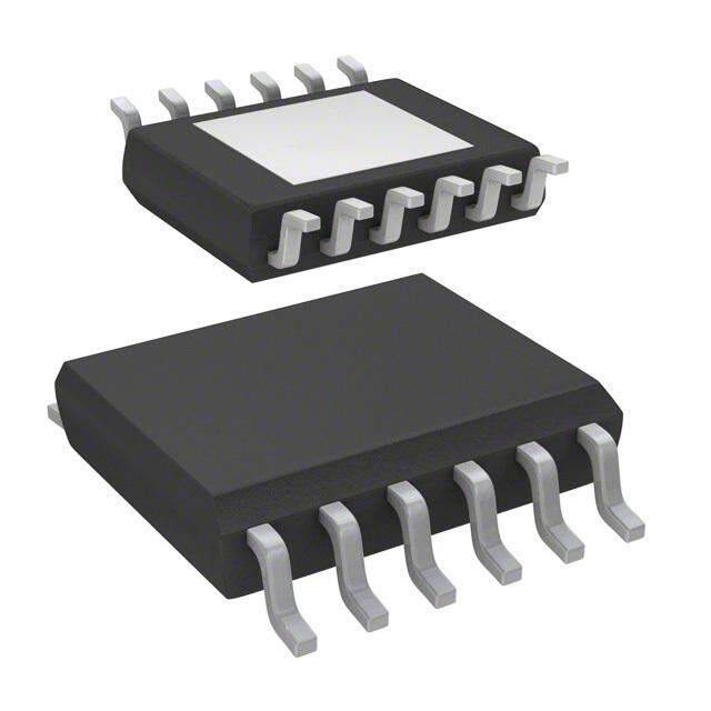
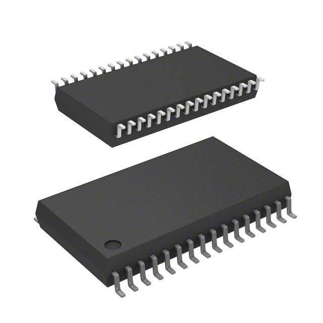
| 供应商器件封装 | PowerSSO-12™ |
| 关闭阈值 | 3.5 V |
| 其它名称 | 497-11694-1 |
| 其它有关文件 | http://www.st.com/web/catalog/sense_power/FM1965/CL1969/SC1037/PF152027?referrer=70071840 |
| 包装 | 剪切带 (CT) |
| 商标 | STMicroelectronics |
| 安装类型 | 表面贴装 |
| 安装风格 | SMD/SMT |
| 导通电阻 | 160 毫欧 |
| 封装 | Reel |
| 封装/外壳 | 12-LSOP(0.154",3.90mm 宽)裸焊盘 |
| 封装/箱体 | PowerSSO-12 |
| 工作温度 | - 40 C to + 150 C |
| 工作电源电压 | 36 V |
| 工厂包装数量 | 2500 |
| 标准包装 | 1 |
| 电压-电源 | 4.5 V ~ 36 V |
| 电流-峰值输出 | 5A |
| 电流-输出/通道 | 3.5A |
| 电源电流 | 6 mA |
| 类型 | Automotive High Side Driver |
| 系列 | VND5160J-E |
| 输入类型 | 非反相 |
| 输出数 | 2 |
| 输出端数量 | 2 |


- 商务部:美国ITC正式对集成电路等产品启动337调查
- 曝三星4nm工艺存在良率问题 高通将骁龙8 Gen1或转产台积电
- 太阳诱电将投资9.5亿元在常州建新厂生产MLCC 预计2023年完工
- 英特尔发布欧洲新工厂建设计划 深化IDM 2.0 战略
- 台积电先进制程称霸业界 有大客户加持明年业绩稳了
- 达到5530亿美元!SIA预计今年全球半导体销售额将创下新高
- 英特尔拟将自动驾驶子公司Mobileye上市 估值或超500亿美元
- 三星加码芯片和SET,合并消费电子和移动部门,撤换高东真等 CEO
- 三星电子宣布重大人事变动 还合并消费电子和移动部门
- 海关总署:前11个月进口集成电路产品价值2.52万亿元 增长14.8%


PDF Datasheet 数据手册内容提取
VND5160J-E Double channel high side driver for automotive applications Features Max supply voltage V 41V CC Operating voltage range V 4.5 to 36V CC PowerSSO-12 Max on-state resistance R 160 m ON Current limitation (typ) I 5A – Electrostatic discharge protection LIMH Off state supply current (typ) I 2 µA(1) S Application 1. Typical value with all loads connected. ■ General ■ All types of resistive, inductive and capacitive – Inrush current active management by loads power limitation – Very low stand-by current Description – 3.0V CMOS compatible input The VND5160J-E is a monolithic device made – Optimized electromagnetic emission using STMicroelectronics VIPower M0-5 – Very low electromagnetic susceptibility technology. It is intended for driving resistive or – In compliance with the 2002/95/EC inductive loads with one side connected to European directive ground. Active V pin voltage clamp protects the CC ■ Diagnostic functions device against low energy spikes (see ISO7637 transient compatibility table). – Open drain status output – On state open load detection The device detects open load condition in both – Off state open load detection ON and OFF states, when STAT_DIS is left open or driven low. Output shorted to V is detected in – Thermal shutdown indication CC the OFF state. ■ Protection When STAT_DIS is driven high, the STATUS pin is – Undervoltage shut-down in a high impedance condition. – Overvoltage clamp – Output stuck to Vcc detection Output current limitation protects the device in – Load current limitation overload condition. In case of long duration – Self limiting of fast thermal transients overload, the device limits the dissipated power to safe level up to thermal shut-down intervention. – Protection against loss of ground and loss Thermal shut-down with automatic restart allows of V CC the device to recover normal operation as soon as – Thermal shut down fault condition disappears. – Reverse battery protection (see Figure28) Table 1. Device summary Order codes Package Part number (Tube) Part number (Tape & Reel) PowerSSO-12 VND5160J-E VND5160JTR-E September 2013 Rev 6 1/31 www.st.com 31
Contents VND5160J-E Contents 1 Block diagram and pin description . . . . . . . . . . . . . . . . . . . . . . . . . . . . . 5 2 Electrical specifications . . . . . . . . . . . . . . . . . . . . . . . . . . . . . . . . . . . . . . 7 2.1 Absolute maximum ratings . . . . . . . . . . . . . . . . . . . . . . . . . . . . . . . . . . . . . 7 2.2 Thermal data . . . . . . . . . . . . . . . . . . . . . . . . . . . . . . . . . . . . . . . . . . . . . . . 8 2.3 Electrical characteristics . . . . . . . . . . . . . . . . . . . . . . . . . . . . . . . . . . . . . . . 9 2.4 Electrical characteristics curves . . . . . . . . . . . . . . . . . . . . . . . . . . . . . . . . 16 3 Application information . . . . . . . . . . . . . . . . . . . . . . . . . . . . . . . . . . . . . 20 3.1 GND protection network against reverse battery . . . . . . . . . . . . . . . . . . . 20 3.1.1 Solution 1 : resistor in the ground line (RGND only) . . . . . . . . . . . . . . . 20 3.1.2 Solution 2: a diode (DGND) in the ground line . . . . . . . . . . . . . . . . . . . 21 3.2 Load dump protection . . . . . . . . . . . . . . . . . . . . . . . . . . . . . . . . . . . . . . . . 21 3.3 MCU I/Os protection . . . . . . . . . . . . . . . . . . . . . . . . . . . . . . . . . . . . . . . . . 21 3.4 Open load detection in Off state . . . . . . . . . . . . . . . . . . . . . . . . . . . . . . . . 21 3.5 Maximum demagnetization energy (VCC = 13.5V) . . . . . . . . . . . . . . . . . 23 4 Package and PCB thermal data . . . . . . . . . . . . . . . . . . . . . . . . . . . . . . . 24 4.1 PowerSSO-12™ thermal data . . . . . . . . . . . . . . . . . . . . . . . . . . . . . . . . . 24 5 Package information . . . . . . . . . . . . . . . . . . . . . . . . . . . . . . . . . . . . . . . . 27 5.1 ECOPACK® packages . . . . . . . . . . . . . . . . . . . . . . . . . . . . . . . . . . . . . . . 27 5.2 PowerSSO-12™ package information . . . . . . . . . . . . . . . . . . . . . . . . . . . 27 5.3 Packing information . . . . . . . . . . . . . . . . . . . . . . . . . . . . . . . . . . . . . . . . . 29 6 Revision history . . . . . . . . . . . . . . . . . . . . . . . . . . . . . . . . . . . . . . . . . . . 30 2/31
VND5160J-E List of tables List of tables Table 1. Device summary. . . . . . . . . . . . . . . . . . . . . . . . . . . . . . . . . . . . . . . . . . . . . . . . . . . . . . . . . . 1 Table 2. Pin functions. . . . . . . . . . . . . . . . . . . . . . . . . . . . . . . . . . . . . . . . . . . . . . . . . . . . . . . . . . . . . 5 Table 3. Suggested connections for unused and N.C. pins . . . . . . . . . . . . . . . . . . . . . . . . . . . . . . . . 6 Table 4. Absolute maximum ratings. . . . . . . . . . . . . . . . . . . . . . . . . . . . . . . . . . . . . . . . . . . . . . . . . . 7 Table 5. Thermal data. . . . . . . . . . . . . . . . . . . . . . . . . . . . . . . . . . . . . . . . . . . . . . . . . . . . . . . . . . . . . 8 Table 6. Power section. . . . . . . . . . . . . . . . . . . . . . . . . . . . . . . . . . . . . . . . . . . . . . . . . . . . . . . . . . . . 9 Table 7. Switching (VCC=13V; Tj=25°C) . . . . . . . . . . . . . . . . . . . . . . . . . . . . . . . . . . . . . . . . . . . . 9 Table 8. Status pin (V =0) . . . . . . . . . . . . . . . . . . . . . . . . . . . . . . . . . . . . . . . . . . . . . . . . . . . . . . . 10 SD Table 9. Protection . . . . . . . . . . . . . . . . . . . . . . . . . . . . . . . . . . . . . . . . . . . . . . . . . . . . . . . . . . . . . . 10 Table 10. Openload detection. . . . . . . . . . . . . . . . . . . . . . . . . . . . . . . . . . . . . . . . . . . . . . . . . . . . . . . 11 Table 11. Logic input . . . . . . . . . . . . . . . . . . . . . . . . . . . . . . . . . . . . . . . . . . . . . . . . . . . . . . . . . . . . . 11 Table 12. Truth table. . . . . . . . . . . . . . . . . . . . . . . . . . . . . . . . . . . . . . . . . . . . . . . . . . . . . . . . . . . . . . 13 Table 13. Electrical transient requirements . . . . . . . . . . . . . . . . . . . . . . . . . . . . . . . . . . . . . . . . . . . . 14 Table 14. Thermal parameters. . . . . . . . . . . . . . . . . . . . . . . . . . . . . . . . . . . . . . . . . . . . . . . . . . . . . . 26 Table 15. PowerSSO-12™ mechanical data . . . . . . . . . . . . . . . . . . . . . . . . . . . . . . . . . . . . . . . . . . . 28 Table 16. Document revision history . . . . . . . . . . . . . . . . . . . . . . . . . . . . . . . . . . . . . . . . . . . . . . . . . 30 3/31
List of figures VND5160J-E List of figures Figure 1. Block diagram. . . . . . . . . . . . . . . . . . . . . . . . . . . . . . . . . . . . . . . . . . . . . . . . . . . . . . . . . . . . 5 Figure 2. Configuration diagram (top view) . . . . . . . . . . . . . . . . . . . . . . . . . . . . . . . . . . . . . . . . . . . . . 6 Figure 3. Current and voltage conventions . . . . . . . . . . . . . . . . . . . . . . . . . . . . . . . . . . . . . . . . . . . . . 7 Figure 4. Status timings. . . . . . . . . . . . . . . . . . . . . . . . . . . . . . . . . . . . . . . . . . . . . . . . . . . . . . . . . . . 12 Figure 5. Output voltage drop limitation. . . . . . . . . . . . . . . . . . . . . . . . . . . . . . . . . . . . . . . . . . . . . . . 12 Figure 6. Switching characteristics . . . . . . . . . . . . . . . . . . . . . . . . . . . . . . . . . . . . . . . . . . . . . . . . . . 13 Figure 7. Waveforms . . . . . . . . . . . . . . . . . . . . . . . . . . . . . . . . . . . . . . . . . . . . . . . . . . . . . . . . . . . . . 15 Figure 8. Off state output current. . . . . . . . . . . . . . . . . . . . . . . . . . . . . . . . . . . . . . . . . . . . . . . . . . . . 16 Figure 9. Input clamp voltage. . . . . . . . . . . . . . . . . . . . . . . . . . . . . . . . . . . . . . . . . . . . . . . . . . . . . . . 16 Figure 10. High level input current. . . . . . . . . . . . . . . . . . . . . . . . . . . . . . . . . . . . . . . . . . . . . . . . . . . . 16 Figure 11. Input high level . . . . . . . . . . . . . . . . . . . . . . . . . . . . . . . . . . . . . . . . . . . . . . . . . . . . . . . . . . 16 Figure 12. Input low level. . . . . . . . . . . . . . . . . . . . . . . . . . . . . . . . . . . . . . . . . . . . . . . . . . . . . . . . . . . 16 Figure 13. Input hysteresis voltage . . . . . . . . . . . . . . . . . . . . . . . . . . . . . . . . . . . . . . . . . . . . . . . . . . . 16 Figure 14. Status low output voltage . . . . . . . . . . . . . . . . . . . . . . . . . . . . . . . . . . . . . . . . . . . . . . . . . . 17 Figure 15. Status leakage current . . . . . . . . . . . . . . . . . . . . . . . . . . . . . . . . . . . . . . . . . . . . . . . . . . . . 17 Figure 16. Status clamp voltage . . . . . . . . . . . . . . . . . . . . . . . . . . . . . . . . . . . . . . . . . . . . . . . . . . . . . 17 Figure 17. On state resistance vs Tcase . . . . . . . . . . . . . . . . . . . . . . . . . . . . . . . . . . . . . . . . . . . . . 17 Figure 18. On state resistance vs VCC . . . . . . . . . . . . . . . . . . . . . . . . . . . . . . . . . . . . . . . . . . . . . . 17 Figure 19. Openload On state detection threshold . . . . . . . . . . . . . . . . . . . . . . . . . . . . . . . . . . . . . . . 17 Figure 20. Openload Off state voltage detection threshold . . . . . . . . . . . . . . . . . . . . . . . . . . . . . . . . . 18 Figure 21. Turn - On voltage slope . . . . . . . . . . . . . . . . . . . . . . . . . . . . . . . . . . . . . . . . . . . . . . . . . . . 18 Figure 22. Turn - Off voltage slope . . . . . . . . . . . . . . . . . . . . . . . . . . . . . . . . . . . . . . . . . . . . . . . . . . . 18 Figure 23. ILIM vs Tcase. . . . . . . . . . . . . . . . . . . . . . . . . . . . . . . . . . . . . . . . . . . . . . . . . . . . . . . . . . 18 Figure 24. Undervoltage shutdown . . . . . . . . . . . . . . . . . . . . . . . . . . . . . . . . . . . . . . . . . . . . . . . . . . . 18 Figure 25. STAT_DIS clamp voltage. . . . . . . . . . . . . . . . . . . . . . . . . . . . . . . . . . . . . . . . . . . . . . . . . . 18 Figure 26. High level STAT_DIS voltage. . . . . . . . . . . . . . . . . . . . . . . . . . . . . . . . . . . . . . . . . . . . . . . 19 Figure 27. Low level STAT_DIS voltage . . . . . . . . . . . . . . . . . . . . . . . . . . . . . . . . . . . . . . . . . . . . . . . 19 Figure 28. Application schematic. . . . . . . . . . . . . . . . . . . . . . . . . . . . . . . . . . . . . . . . . . . . . . . . . . . . . 20 Figure 29. Open load detection in Off state. . . . . . . . . . . . . . . . . . . . . . . . . . . . . . . . . . . . . . . . . . . . . 22 Figure 30. Maximum turn Off current versus inductance (for each channel). . . . . . . . . . . . . . . . . . . . 23 Figure 31. PowerSSO-12™ PC board. . . . . . . . . . . . . . . . . . . . . . . . . . . . . . . . . . . . . . . . . . . . . . . . . 24 Figure 32. Rthj-amb vs. PCB copper area in open box free air condition (one channel ON). . . . . . . . 24 Figure 33. PowerSSO-12™ Thermal impedance junction ambient single pulse (one channel ON) . . 25 Figure 34. Thermal fitting model of a double channel HSD in PowerSSO-12™ . . . . . . . . . . . . . . . . . 25 Figure 35. PowerSSO-12™ package dimensions. . . . . . . . . . . . . . . . . . . . . . . . . . . . . . . . . . . . . . . . 27 Figure 36. PowerSSO-12™ tube shipment (no suffix). . . . . . . . . . . . . . . . . . . . . . . . . . . . . . . . . . . . . 29 Figure 37. PowerSSO-12™ tape and reel shipment (suffix “TR”) . . . . . . . . . . . . . . . . . . . . . . . . . . . . 29 4/31
VND5160J-E Block diagram and pin description 1 Block diagram and pin description Figure 1. Block diagram VCC OUTPUT1 GND VCC CLAMP UNDERVOLTAGE INPUT1 STATUS1 CLAMP 1 CLAMP 2 STAT_DIS DRIVER 1 DRIVER 2 INPUT2 LOGIC ILIM 1 ILIM 2 PWRLIM1 VDSLIM 1 VDSLIM 2 STATUS2 OPENLOAD ON 1 OPENLOAD ON 2 OVERTEMP. 1 OVERTEMP. 2 OPENLOAD OFF 1 OPENLOAD OFF 2 OUTPUT2 PWRLIM 2 Table 2. Pin functions Name Function V Battery connection. CC OUTPUTn Power output. Ground connection. Must be reverse battery protected by an external diode/ GND resistor network. Voltage controlled input pin with hysteresis, CMOS compatible. Controls output INPUTn switch state. STATUSn Open Drain digital diagnostic pin. STAT_DIS Active high CMOS compatible pin, to disable the STATUS pin. 5/31
Block diagram and pin description VND5160J-E Figure 2. Configuration diagram (top view) TAB = V cc GND V 1 12 cc STAT_DIS 2 11 OUTPUT 1 INPUT 1 3 10 OUTPUT 1 STATUS 1 4 9 OUTPUT 2 STATUS 2 5 8 OUTPUT 2 6 7 INPUT 2 V cc Table 3. Suggested connections for unused and N.C. pins Connection / Pin STATUS N.C. OUTPUT INPUT STAT_DIS Floating X X X X X Through 10k Through 10k To ground N.R.(1) X N.R. resistor resistor 1. Not recommended. 6/31
VND5160J-E Electrical specifications 2 Electrical specifications Figure 3. Current and voltage conventions I S V CC V V CC Fn I I OUTn SD STAT_DIS OUTPUTn V V SD OUTn I I INn STATn INPUTn STATUSn V V INn STATn GND I GND Note: V = V - V during reverse battery condition. Fn OUTn CCn 2.1 Absolute maximum ratings Stressing the device above the ratings listed in the “Absolute maximum ratings” tables may cause permanent damage to the device. These are stress ratings only and operation of the device at these or any other conditions above those indicated in the Operating sections of this specification is not implied. Exposure to the conditions in this section for extended periods may affect device reliability. Refer also to the STMicroelectronics SURE Program and other relevant quality documents. T able 4. Absolute maximum ratings Symbol Parameter Value Unit V DC supply voltage 41 V CC -V Reverse DC supply voltage 0.3 V CC -I DC reverse ground pin current 200 mA GND I DC output current Internally limited A OUT -I Reverse DC output current 6 A OUT I DC input current +10 / -1 mA IN I DC status current +10 / -1 mA STAT I DC status disable current +10 / -1 mA STAT_DIS Maximum switching energy E (L=12mH; R =0; V =13.5V; T =150°C; 33 mJ MAX L bat jstart I = I (Typ.) ) OUT limL 7/31
Electrical specifications VND5160J-E Table 4. Absolute maximum ratings (continued) Symbol Parameter Value Unit Electrostatic discharge (Human Body Model: R=1.5K C=100pF) – INPUT 4000 V V – STATUS 4000 V ESD – STAT_DIS 4000 V – OUTPUT 5000 V – VCC 5000 V V Charge device model (CDM-AEC-Q100-011) 750 V ESD T Junction operating temperature -40 to 150 °C j T Storage temperature -55 to 150 °C stg 2.2 Thermal data Table 5. Thermal data Symbol Parameter Max value Unit R Thermal resistance junction-case (max.) (with one channel ON) 8 °C/W thj-case R Thermal resistance junction-ambient See Figure32 °C/W thj-amb 8/31
VND5160J-E Electrical specifications 2.3 Electrical characteristics Values specified in this section are for 8V<V <36V; -40°C<T<150°C, unless otherwise CC j stated. T a . ble 6. Power section Symbol Parameter Test conditions Min. Typ. Max. Unit V Operating supply voltage 4.5 13 36 V CC V Undervoltage shutdown 3.5 4.5 V USD Undervoltage Shut-down V 0.5 V USDhyst hysteresis I = 1A; T= 25°C 160 m OUT j R On state resistance(2) I = 1A; T= 150°C 320 m ON OUT j I = 1A; V = 5V; T= 25°C 210 m OUT CC j V Clamp voltage I = 20mA 41 46 52 V clamp S Off State; V =13V; V =V =0 CC IN OUT T=25°C; I Supply current j 2(1) 5(1) µA S On State; V =13V; V =5V; CC IN 3 6 mA I =0A OUT V =V =0V; V =13V; T=25°C 0 0.01 3 I IN OUT CC j L(off1) Off state output current(2) VIN=VOUT=0V; VCC=13V; Tj=125°C 0 5 µA I V =0V; V =4V -75 0 L(off2) IN OUT Output - V diode V CC -I =0.6A; T=150°C 0.7 V F voltage(2) OUT j 1. PowerMOS leakage included. 2. For each channel. T able 7. Switching (V =13V; T =25°C) CC j Symbol Parameter Test conditions Min. Typ. Max. Unit t Turn-On delay time R =13 (see Figure6) 10 µs d(on) L t Turn-Off delay time R =13(see Figure6) 15 µs d(off) L dV /dt Turn-On voltage slope R =13 See Figure21 Vµs OUT (on) L dV /dt Turn-Off voltage slope R =13 See Figure22 Vµs OUT (off) L W Switching energy losses during t R =13(see Figure6) 0.07 mJ ON won L W Switching energy losses during t R =13(see Figure6) 0.04 mJ OFF woff L 9/31
Electrical specifications VND5160J-E Table 8. Status pin (V =0) SD Symbol Parameter Test conditions Min. Typ. Max. Unit V Status low output voltage I = 1.6 mA, V =0V 0.5 V STAT STAT SD Normal operation or V =5V, I Status leakage current SD 10 µA LSTAT V = 5V STAT Normal operation or V =5V, C Status pin input capacitance SD 100 pF STAT V = 5V STAT I = 1mA 5.5 7 V V Status clamp voltage STAT SCL I = - 1mA -0.7 V STAT T able 9. Protection(1) Symbol Parameter Test conditions Min. Typ. Max. Unit V = 13V 3.5 5 7.5 A I DC short circuit current CC limH 5V<V <36V 7.5 A CC Short circuit current during I V = 13V T <T<T 2 A limL thermal cycling CC R j TSD T Shutdown temperature 150 175 200 °C TSD T Reset temperature T + 1 T + 5 °C R RS RS T Thermal reset of STATUS 135 °C RS T Thermal hysteresis (T -T ) 7 °C HYST TSD R Status delay in overload t T>T 20 µs SDL conditions j TSD Turn-Off output voltage V I =1A; V =0; L=20mH V -41 V -46 V -52 V DEMAG clamp OUT IN CC CC CC I = 0.03A; Output voltage drop OUT V T= -40°C...+150°C 25 mV ON limitation j (see Figure5) 1. To ensure long term reliability under heavy overload or short circuit conditions, protection and related diagnostic signals must be used together with a proper software strategy. If the device is subjected to abnormal conditions, this software must limit the duration and number of activation cycles. 10/31
VND5160J-E Electrical specifications T able 10. Openload detection Symbol Parameter Test conditions Min. Typ. Max. Unit Openload On state See I V = 5V, 8V<V <18V 10 40 mA OL detection threshold IN CC Figure19 Openload On state I = 0A, V =13V t OUT CC 200 µs DOL(on) detection delay (see Figure4) Delay between INPUT falling t edge and STATUS rising I = 0A (see Figure4) 200 500 1000 µs POL OUT edge in Openload condition Openload Off state voltage See V V = 0V, 8V<V <16V 2 4 V OL detection threshold IN CC Figure20 Output short circuit to V t cc See Figure4 180 t µs DSTKON detection delay at turn Off POL T able 11. Logic input Symbol Parameter Test conditions Min. Typ. Max. Unit V Input low level voltage 0.9 V IL I Low level input current V = 0.9V 1 µA IL IN V Input high level voltage 2.1 V IH I High level input current V = 2.1V 10 µA IH IN V Input hysteresis voltage 0.25 V I(hyst) I = 1mA 5.5 7 V V Input clamp voltage IN ICL I = -1mA -0.7 V IN V STAT_DIS low level voltage 0.9 V SDL I Low level STAT_DIS current V = 0.9V 1 µA SDL CSD V STAT_DIS high level voltage 2.1 V SDH I High level STAT_DIS current V = 2.1V 10 µA SDH CSD V STAT_DIS hysteresis voltage 0.25 V SD(hyst) I = 1mA 5.5 7 V V STAT_DIS clamp voltage SD SDCL I = -1mA -0.7 V SD 11/31
Electrical specifications VND5160J-E Figure 4. Status timings OPEN LOAD STATUS TIMING (without external pull-up) OPEN LOAD STATUS TIMING (with external pull-up) VIN IOUT < IOL VIN IOUT < IOL VOUT < VOL VOUT > VOL VSTAT VSTAT tDOL(on) tPOL tDOL(on) OUTPUT STUCK TO Vcc OVER TEMP STATUS TIMING VIN IOUT > IOL Tj > TTSD VOUT > VOL VIN VSTAT VSTAT tDOL(on) tDSTKON tSDL tSDL Figure 5. Output voltage drop limitation V -V cc out Tj=150oC Tj=25oC Tj=-40oC V on I out V /R on on(T) 12/31
VND5160J-E Electrical specifications T able 12. Truth table Conditions INPUT OUTPUT STATUS (V =0V)(1) n n n SD L L H Normal operation H H H L L H Current limitation H X H L L H Overtemperature H L L L L X Undervoltage H L X L H L(2) Output Voltage > V OL H H H L L H(3) Output Current < I OL H H L 1. If the V is high, the STATUS pin is in a high impedance. SD 2. The STATUS pin is low with a delay equal to t after INPUT falling edge. DSTKON 3. The STATUS pin becomes high with a delay equal to t after INPUT falling edge. POL Figure 6. Switching characteristics VOUT tWon tWoff 90% 80% dVOUT/dt(on) dVOUT/dt(off) tr 10% tf t INPUT td(on) td(off) t 13/31
Electrical specifications VND5160J-E T able 13. Electrical transient requirements ISO 7637-2: Test levels(1) Number of Burst cycle/pulse Delays and 2004(E) pulses or repetition time impedance test pulse III IV test times 1 -75V -100V 5000 pulses 0.5 s 5 s 2 ms, 10 2a +37V +50V 5000 pulses 0.2 s 5 s 50 µs, 2 3a -100V -150V 1h 90 ms 100 ms 0.1 µs, 50 3b +75V +100V 1h 90 ms 100 ms 0.1 µs, 50 4 -6V -7V 1 pulse 100 ms, 0.01 5b(2) +65V +87V 1 pulse 400 ms, 2 ISO 7637-2: Test level results(1) 2004(E) test pulse III IV 1 C C 2a C C 3a C C 3b C C 4 C C 5b(2) C C 1. The above test levels must be considered referred to VCC = 13.5V except for pulse 5b. 2. Valid in case of external load dump clamp: 40V maximum referred to ground. Class Contents C All functions of the device are performed as designed after exposure to disturbance. One or more functions of the device are not performed as designed after exposure to E disturbance and cannot be returned to proper operation without replacing the device. 14/31
VND5160J-E Electrical specifications Figure 7. Waveforms NORMAL OPERATION INPUT STAT_DIS LOAD CURRENT STATUS UNDERVOLTAGE VUSDhyst VCC VUSD INPUT STAT_DIS LOAD CURRENT STATUS undefined OPEN LOAD with external pull-up INPUT STAT_DIS LOAD VOLTAGE VOUT>VOL VOL STATUS OPEN LOAD without external pull-up INPUT STAT_DIS LOAD VOLTAGE LOAD CURRENT IOUT<IOL tPOL STATUS RESISTIVE SHORT TO Vcc, NORMAL LOAD INPUT STAT_DIS LOAD VOLTAGE IOUT>IOL VOUT>VOL VOL STATUS tDSTKON OVERLOAD OPERATION Tj TR TTSD TRS INPUT STAT_DIS LOAD CURRENT IILLIIMMHL STATUS current power thermal cycling limitation limitation SHORTED LOAD NORMAL LOAD 15/31
Electrical specifications VND5160J-E 2.4 Electrical characteristics curves Figure 8. Off state output current Figure 9. Input clamp voltage Iloff1 (uA) Vicl (V) 8 0.25 Off state 7.75 Vcc=13V Iin=1mA Vin=Vout=0V 7.5 0.2 7.25 0.15 7 0.1 6.75 6.5 0.05 6.25 0 6 -50 -25 0 25 50 75 100 125 150 175 -50 -25 0 25 50 75 100 125 150 175 Tc (°C) Tc (°C) Figure 10. High level input current Figure 11. Input high level Iih (uA) Vih (V) 5 4 4.5 3.5 Vin=2.1V 4 3 3.5 2.5 3 2.5 2 2 1.5 1.5 1 1 0.5 0.5 0 0 -50 -25 0 25 50 75 100 125 150 175 -50 -25 0 25 50 75 100 125 150 175 Tc (°C) Tc (°C) Figure 12. Input low level Figure 13. Input hysteresis voltage Vil (V) Vihyst (V) 4 2 3.5 1.75 3 1.5 2.5 1.25 2 1 1.5 0.75 1 0.5 0.5 0.25 0 0 -50 -25 0 25 50 75 100 125 150 175 -50 -25 0 25 50 75 100 125 150 175 Tc (°C) Tc (°C) 16/31
VND5160J-E Electrical specifications Figure 14. Status low output voltage Figure 15. Status leakage current Vstat (V) Ilstat (uA) 0.9 0.08 0.8 0.072 Istat=1.6mA 0.7 Vstat=5V 0.064 0.6 0.5 0.056 0.4 0.048 0.3 0.04 0.2 0.032 0.1 0 -50 -25 0 25 50 75 100 125 150 175 -50 -25 0 25 50 75 100 125 150 175 Tc (°C) Tc (°C) Figure 16. Status clamp voltage Figure 17. On state resistance vs T case Vscl (V) Ron (mOhm) 9 300 8.5 270 Istat=1mA Iout=1A 8 240 Vcc=13V 7.5 210 7 180 6.5 150 6 120 5.5 90 5 60 4.5 30 4 0 -50 -25 0 25 50 75 100 125 150 175 -50 -25 0 25 50 75 100 125 150 175 Tc (°C) Tc (°C) Figure 18. On state resistance vs V Figure 19. Openload On state detection CC threshold Ron (mOhm) Iol (mA) 300 100 275 Tc=150°C 90 Vin=5V 250 80 Tc=125°C 225 70 200 60 175 50 150 Tc=25°C 40 125 30 Tc=-40°C 100 20 75 10 50 0 0 5 10 15 20 25 30 35 40 -50 -25 0 25 50 75 100 125 150 175 Vcc (V) Tc (°C) 17/31
Electrical specifications VND5160J-E Figure 20. Openload Off state voltage Figure 21. Turn - On voltage slope detection threshold Vol (V) dVout/dt(on) (V/ms) 5 1000 4.5 900 Vin=0V Vcc=13V 4 800 Ri=6.5Ohm 3.5 700 3 600 2.5 500 2 400 1.5 300 1 200 0.5 100 0 0 -50 -25 0 25 50 75 100 125 150 175 -50 -25 0 25 50 75 100 125 150 175 Tc (°C) Tc (°C) Figure 22. Turn - Off voltage slope Figure 23. I vs T LIM case dVout/dt(off) (V/ms) Ilimh (A) 1000 10 900 9 800 8 Vcc=13V 700 7 Vcc=13V 600 6 Ri=13Ohm 500 5 400 4 300 3 200 2 100 1 0 0 -50 -25 0 25 50 75 100 125 150 175 -50 -25 0 25 50 75 100 125 150 175 Tc (°C) Tc (°C) Figure 24. Undervoltage shutdown Figure 25. STAT_DIS clamp voltage Vusd (V) Vsdcl (V) 14 14 12 12 Isd=1mA 10 10 8 8 6 6 4 4 2 2 0 0 -50 -25 0 25 50 75 100 125 150 175 -50 -25 0 25 50 75 100 125 150 175 Tc (°C) Tc (°C) 18/31
VND5160J-E Electrical specifications Figure 26. High level STAT_DIS voltage Figure 27. Low level STAT_DIS voltage Vsdh (V) Vsdl (V) 8 8 7 7 6 6 5 5 4 4 3 3 2 2 1 1 0 0 -50 -25 0 25 50 75 100 125 150 175 -50 -25 0 25 50 75 100 125 150 175 Tc (°C) Tc (°C) 19/31
Application information VND5160J-E 3 Application information Figure 28. Application schematic +5V +5V VCC Rprot STAT_DIS Dld Rprot INPUT µC OUTPUT Rprot STATUS GND RGND VGND DGND Note: Channels 2, has the same internal circuit as channel 1. 3.1 GND protection network against reverse battery 3.1.1 Solution 1 : resistor in the ground line (R only) GND This can be used with any type of load. The following is an indication on how to dimension the R resistor. GND 1. R 600mV / (I ). GND S(on)max 2. R V ) / (-I ) GND CC GND where -I is the DC reverse ground pin current and can be found in the absolute GND maximum rating section of the device datasheet. Power Dissipation in R (when V <0: during reverse battery situations) is: GND CC P = (-V )2/R D CC GND This resistor can be shared amongst several different HSDs. Please note that the value of this resistor should be calculated with formula (1) where I becomes the sum of the S(on)max maximum on-state currents of the different devices. Please note that if the microprocessor ground is not shared by the device ground then the R will produce a shift (I * R ) in the input thresholds and the status output GND S(on)max GND values. This shift will vary depending on how many devices are ON in the case of several high side drivers sharing the same R . GND 20/31
VND5160J-E Application information If the calculated power dissipation leads to a large resistor or several devices have to share the same resistor then ST suggests to utilize Solution 2 (see below). 3.1.2 Solution 2: a diode (D ) in the ground line GND A resistor (R =1kshould be inserted in parallel to D if the device drives an GND GND inductive load. This small signal diode can be safely shared amongst several different HSDs. Also in this case, the presence of the ground network will produce a shift (600mV) in the input threshold and in the status output values if the microprocessor ground is not common to the device ground. This shift will not vary if more than one HSD shares the same diode/resistor network. 3.2 Load dump protection D is necessary (Voltage transient suppressor) if the load dump peak voltage exceeds the ld V max DC rating. The same applies if the device is subject to transients on the V line CC CC that are greater than the ones shown in the ISO 7637-2: 2004(E) table. 3.3 MCU I/Os protection If a ground protection network is used and negative transient are present on the V line, CC the control pins will be pulled negative. ST suggests to insert a resistor (R ) in line to prot prevent the µC I/Os pins to latch-up. The value of these resistors is a compromise between the leakage current of C and the current required by the HSD I/Os (Input levels compatibility) with the latch-up limit of C I/Os. -V /I R (V -V -V ) / I CCpeak latchup prot OHC IH GND IHmax Calculation example: For V = - 100V and I 20mA; V 4.5V CCpeak latchup OHC 5k R 180k. prot Recommended R values is 10k prot 3.4 Open load detection in Off state Off state open load detection requires an external pull-up resistor (R ) connected between PU OUTPUT pin and a positive supply voltage (V ) like the +5V line used to supply the PU microprocessor. The external resistor has to be selected according to the following requirements: 1. no false open load indication when load is connected: in this case we have to avoid V to be higher than V ; this results in the following condition OUT Olmin V =(V /(R +R ))R <V . OUT PU L PU L Olmin 2. no misdetection when load is disconnected: in this case the V has to be higher than out V ; this results in the following condition R <(V –V )/I . OLmax PU PU OLmax L(off2) 21/31
Application information VND5160J-E Because I may significantly increase if V is pulled high (up to several mA), the pull- s(OFF) out up resistor R should be connected to a supply that is switched OFF when the module is in PU standby. The values of V , V and I are available in the Electrical characteristics OLmin OLmax L(off2) section. Figure 29. Open load detection in Off state V batt. VPU VCC RPU DRIVER INPUT + IL(off2) LOGIC OUT + R - STATUS VOL RL GROUND 22/31
VND5160J-E Application information 3.5 Maximum demagnetization energy (V = 13.5V) CC Figure 30. Maximum turn Off current versus inductance (for each channel) 10 A B C 1 A) I ( 0,1 0,1 1 L (mH) 10 100 A: T =150°C single pulse jstart B: T =100°C repetitive pulse jstart C: T =125°C repetitive pulse jstart V , I IN L Demagnetization Demagnetization Demagnetization t Note: Values are generated with R =0 L In case of repetitive pulses, T (at beginning of each demagnetization) of every pulse jstart must not exceed the temperature specified above for curves A and B. 23/31
Package and PCB thermal data VND5160J-E 4 Package and PCB thermal data 4.1 PowerSSO-12™ thermal data Figure 31. PowerSSO-12™ PC board Note: Layout condition of R and Z measurements (PCB: Double layer, Thermal Vias, FR4 th th area= 77mm x 86mm,PCB thickness=1.6mm, Cu thickness=70µm (front and back side), Copper areas: from minimum pad lay-out to 8cm2). Figure 32. R vs. PCB copper area in open box free air condition (one channel thj-amb ON) RTHj_amb(°C/W) 65 60 55 50 45 40 35 30 0 2 4 6 8 10 PCB Cu heatsink area (cm^2) 24/31
VND5160J-E Package and PCB thermal data Figure 33. PowerSSO-12™ Thermal impedance junction ambient single pulse (one channel ON) ZTH (°C/W) 100 Footprint 2 cm2 8 cm2 10 1 0,1 0,0001 0,001 0,01 0,1 1 10 100 1000 Time (s) Pulse calculation formula Z = R +Z 1– TH TH THtp where = t /T P Figure 34. Thermal fitting model of a double channel HSD in PowerSSO-12™(a) a. The fitting model is a semplified thermal tool and is valid for transient evolutions where the embedded protections (power limitation or thermal cycling during thermal shutdown) are not triggered. 25/31
Package and PCB thermal data VND5160J-E T able 14. Thermal parameters Area/island (cm2) Footprint 2 8 R1=R7 (°C/W) 1.2 R2=R8 (°C/W) 6 R3 (°C/W) 7 R4 (°C/W) 10 10 9 R5 (°C/W) 22 15 10 R6 (°C/W) 26 20 15 C1=C7 (W.s/°C) 0.0008 C2=C8 (W.s/°C) 0.0016 C3 (W.s/°C) 0.05 C4 (W.s/°C) 0.2 0.1 0.1 C5 (W.s/°C) 0.27 0.8 1 C6 (W.s/°C) 3 6 9 26/31
VND5160J-E Package and packing information 5 Package and packing information ® 5.1 ECOPACK packages In order to meet environmental requirements, ST offers these devices in ECOPACK® packages. These packages have a Lead-free second-level interconnect. The category of Second-Level Interconnect is marked on the package and on the inner box label, in compliance with JEDEC Standard JESD97. The maximum ratings related to soldering conditions are also marked on the inner box label. ECOPACK is an ST trademark. ECOPACK specifications are available at: www.st.com. 5.2 PowerSSO-12™package information Figure 35. PowerSSO-12™ package dimensions 27/31
Package and packing information VND5160J-E T a ble 15. PowerSSO-12™ mechanical data Millimeters Symbol Min. Typ. Max. A 1.250 1.620 A1 0.000 0.100 A2 1.100 1.650 B 0.230 0.410 C 0.190 0.250 D 4.800 5.000 E 3.800 4.000 e 0.800 H 5.800 6.200 h 0.250 0.500 L 0.400 1.270 k 0° 8° X 1.900 2.500 Y 3.600 4.200 ddd 0.100 28/31
VND5160J-E Package and packing information 5.3 Packing information Figure 36. PowerSSO-12™ tube shipment (no suffix) B Base Q.ty 100 C Bulk Q.ty 2000 Tube length (± 0.5) 532 A 1.85 A B 6.75 C (± 0.1) 0.6 All dimensions are in mm. Figure 37. PowerSSO-12™ tape and reel shipment (suffix “TR”) REEL DIMENSIONS Base Q.ty 2500 Bulk Q.ty 2500 A (max) 330 B (min) 1.5 C (± 0.2) 13 F 20.2 G (+ 2 / -0) 12.4 N (min) 60 T (max) 18.4 TAPE DIMENSIONS According to Electronic Industries Association (EIA) Standard 481 rev. A, Feb. 1986 Tape width W 12 Tape Hole Spacing P0 (± 0.1) 4 Component Spacing P 8 Hole Diameter D (± 0.05) 1.5 Hole Diameter D1 (min) 1.5 Hole Position F (± 0.1) 5.5 Compartment Depth K (max) 4.5 Hole Spacing P1 (± 0.1) 2 All dimensions are in mm. End Start Top No components Components No components cover tape 500mm min 500mm min Empty components pockets saled with cover tape. User direction of feed 29/31
Revision history VND5160J-E 6 Revision history T able 16. Document revision history Date Revision Changes 7-Jan-2004 1 Initial release. 3-Feb-2006 2 Major series of updates incorporated. Reformatted. Added list of tables and list of figures. 20-Mar-2007 3 Added Section3.5: Maximum demagnetization energy (VCC=13.5V). Added new disclaimer. Updated Table4: Absolute maximum ratings: EMAX entries. Updated Table13: Electrical transient requirements :Test level 01-Jun-2007 4 values III and IV for test pulse 5b and notes. Figure34: Thermal fitting model of a double channel HSD in PowerSSO-12™ added note. Updated Section4.1: PowerSSO-12™ thermal data: – Changed Figure32: Rthj-amb vs. PCB copper area in open box free air condition (one channel ON). – Changed Figure33: PowerSSO-12™ Thermal impedance junction ambient single pulse (one channel ON). – Updated Table14: Thermal parameters: 17-Dic-2007 5 R1 and R7 values changed from 1.2 to 0.1 °C/W. R2 = R8 values changed from 6 to 0.2 °C/W. R3 value changed from 7 to 4 °C/W. R4 values changed from 10/10/9 to 8/8/7 °C/W. C1=C7 values changed from 0.0008 to 0.0001 °C/W. C2=C8 values changed from 0.0016 to 0.002 °C/W. 24-Sep-2013 6 Updated disclaimer. 30/31
VND5160J-E Please Read Carefully: Information in this document is provided solely in connection with ST products. STMicroelectronics NV and its subsidiaries (“ST”) reserve the right to make changes, corrections, modifications or improvements, to this document, and the products and services described herein at any time, without notice. All ST products are sold pursuant to ST’s terms and conditions of sale. Purchasers are solely responsible for the choice, selection and use of the ST products and services described herein, and ST assumes no liability whatsoever relating to the choice, selection or use of the ST products and services described herein. No license, express or implied, by estoppel or otherwise, to any intellectual property rights is granted under this document. If any part of this document refers to any third party products or services it shall not be deemed a license grant by ST for the use of such third party products or services, or any intellectual property contained therein or considered as a warranty covering the use in any manner whatsoever of such third party products or services or any intellectual property contained therein. UNLESS OTHERWISE SET FORTH IN ST’S TERMS AND CONDITIONS OF SALE ST DISCLAIMS ANY EXPRESS OR IMPLIED WARRANTY WITH RESPECT TO THE USE AND/OR SALE OF ST PRODUCTS INCLUDING WITHOUT LIMITATION IMPLIED WARRANTIES OF MERCHANTABILITY, FITNESS FOR A PARTICULAR PURPOSE (AND THEIR EQUIVALENTS UNDER THE LAWS OF ANY JURISDICTION), OR INFRINGEMENT OF ANY PATENT, COPYRIGHT OR OTHER INTELLECTUAL PROPERTY RIGHT. ST PRODUCTS ARE NOT DESIGNED OR AUTHORIZED FOR USE IN: (A) SAFETY CRITICAL APPLICATIONS SUCH AS LIFE SUPPORTING, ACTIVE IMPLANTED DEVICES OR SYSTEMS WITH PRODUCT FUNCTIONAL SAFETY REQUIREMENTS; (B) AERONAUTIC APPLICATIONS; (C) AUTOMOTIVE APPLICATIONS OR ENVIRONMENTS, AND/OR (D) AEROSPACE APPLICATIONS OR ENVIRONMENTS. WHERE ST PRODUCTS ARE NOT DESIGNED FOR SUCH USE, THE PURCHASER SHALL USE PRODUCTS AT PURCHASER’S SOLE RISK, EVEN IF ST HAS BEEN INFORMED IN WRITING OF SUCH USAGE, UNLESS A PRODUCT IS EXPRESSLY DESIGNATED BY ST AS BEING INTENDED FOR “AUTOMOTIVE, AUTOMOTIVE SAFETY OR MEDICAL” INDUSTRY DOMAINS ACCORDING TO ST PRODUCT DESIGN SPECIFICATIONS. PRODUCTS FORMALLY ESCC, QML OR JAN QUALIFIED ARE DEEMED SUITABLE FOR USE IN AEROSPACE BY THE CORRESPONDING GOVERNMENTAL AGENCY. Resale of ST products with provisions different from the statements and/or technical features set forth in this document shall immediately void any warranty granted by ST for the ST product or service described herein and shall not create or extend in any manner whatsoever, any liability of ST. ST and the ST logo are trademarks or registered trademarks of ST in various countries. Information in this document supersedes and replaces all information previously supplied. The ST logo is a registered trademark of STMicroelectronics. All other names are the property of their respective owners. © 2013 STMicroelectronics - All rights reserved STMicroelectronics group of companies Australia - Belgium - Brazil - Canada - China - Czech Republic - Finland - France - Germany - Hong Kong - India - Israel - Italy - Japan - Malaysia - Malta - Morocco - Philippines - Singapore - Spain - Sweden - Switzerland - United Kingdom - United States of America www.st.com 31/31
Mouser Electronics Authorized Distributor Click to View Pricing, Inventory, Delivery & Lifecycle Information: S TMicroelectronics: VND5160JTR-E VND5160J-E