ICGOO在线商城 > 集成电路(IC) > PMIC - 配电开关,负载驱动器 > VN751STR
 Datasheet下载
- 型号: VN751STR
- 制造商: STMicroelectronics
- 库位|库存: xxxx|xxxx
- 要求:
| 数量阶梯 | 香港交货 | 国内含税 |
| +xxxx | $xxxx | ¥xxxx |
查看当月历史价格
查看今年历史价格
VN751STR产品简介:
ICGOO电子元器件商城为您提供VN751STR由STMicroelectronics设计生产,在icgoo商城现货销售,并且可以通过原厂、代理商等渠道进行代购。 VN751STR价格参考。STMicroelectronicsVN751STR封装/规格:PMIC - 配电开关,负载驱动器, 。您可以下载VN751STR参考资料、Datasheet数据手册功能说明书,资料中有VN751STR 详细功能的应用电路图电压和使用方法及教程。
STMicroelectronics的VN751STR是一款PMIC(电源管理集成电路),属于配电开关和负载驱动器类别。该器件主要应用于需要高效、低功耗和高集成度的电源管理场景,以下是其典型应用场景:

 1. 消费电子设备
   - 智能手机和平板电脑:VN751STR可用于管理手机和平板电脑中的多个负载,例如摄像头模块、显示屏背光、传感器等。它能够提供精确的电流控制和快速的开关响应。
   - 可穿戴设备:如智能手表或健身追踪器,VN751STR的低静态电流特性有助于延长电池寿命。

 2. 物联网(IoT)设备
   - 在智能家居、工业自动化和环境监测等IoT应用中,VN751STR可以为传感器、无线模块和其他外围设备供电,同时确保低功耗运行。
   - 支持动态电源分配,适应不同工作模式下的负载需求。

 3. 便携式医疗设备
   - 如脉搏血氧仪、血糖仪或便携式超声设备,VN751STR能够提供稳定的电源输出,并支持多路负载切换,以优化能量使用。

 4. 汽车电子
   - 信息娱乐系统:用于管理音频放大器、显示屏或其他外设的电源供应。
   - 辅助驾驶系统(ADAS):为摄像头、雷达或激光雷达等关键组件提供可靠的电源支持。
   - 车身控制模块(BCM):实现对车窗升降器、座椅调节器等执行器的电源管理。

 5. 工业设备
   - 在工业控制器、PLC(可编程逻辑控制器)或HMI(人机界面)中,VN751STR可以为各种负载(如继电器、小型电机或LED指示灯)提供高效的电源管理。
   - 支持热插拔功能,便于维护和升级。

 6. 通信设备
   - 在路由器、网关或基站中,VN751STR可用于管理射频前端、基带处理器和其他子系统的电源分配。

 核心优势
- 高效率:降低功耗,提高系统整体能效。
- 小尺寸封装:节省PCB空间,适合紧凑型设计。
- 保护功能:内置过流、过温、短路保护,增强系统可靠性。
- 灵活配置:支持多种负载切换和电源管理策略。

综上所述,VN751STR适用于需要高性能电源管理和低功耗特性的各种电子设备,特别适合便携式、嵌入式和智能化应用场景。
| 参数 | 数值 |
| 产品目录 | 集成电路 (IC)半导体 |
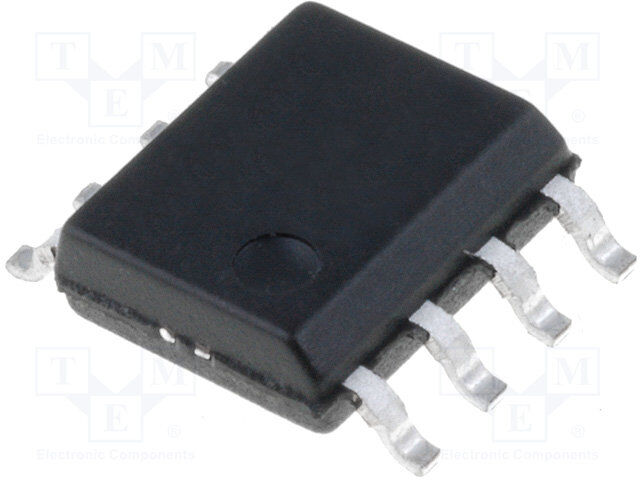
| 描述 | IC DRIVER HIGH SIDE 8-SOIC门驱动器 High Side Driver |
| 产品分类 | PMIC - MOSFET,电桥驱动器 - 内部开关集成电路 - IC |
| 品牌 | STMicroelectronics |
| 产品手册 | |
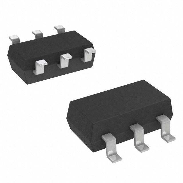
| 产品图片 |
|
| rohs | 符合RoHS无铅 / 符合限制有害物质指令(RoHS)规范要求 |
| 产品系列 | 电源管理 IC,门驱动器,STMicroelectronics VN751STR- |
| 数据手册 | |
| 产品型号 | VN751STR |
| 产品 | Half-Bridge Drivers |
| 产品培训模块 | http://www.digikey.cn/PTM/IndividualPTM.page?site=cn&lang=zhs&ptm=24708 |
| 产品目录页面 | |
| 产品种类 | 门驱动器 |
| 供应商器件封装 | 8-SO |
| 其它名称 | 497-8169-1 |
| 其它有关文件 | http://www.st.com/web/catalog/sense_power/FM142/CL1499/SC903/PF129623?referrer=70071840 |
| 包装 | 剪切带 (CT) |
| 商标 | STMicroelectronics |
| 安装类型 | 表面贴装 |
| 安装风格 | SMD/SMT |
| 导通电阻 | 60 毫欧 |
| 封装 | Reel |
| 封装/外壳 | 8-SOIC(0.154",3.90mm 宽) |
| 封装/箱体 | SO-8 |
| 工作温度 | -40°C ~ 125°C |
| 工厂包装数量 | 2500 |
| 最大关闭延迟时间 | 35000 ns |
| 最大工作温度 | + 150 C |
| 最大开启延迟时间 | 12000 ns |
| 最小工作温度 | - 40 C |
| 标准包装 | 1 |
| 激励器数量 | 1 Driver |
| 电压-电源 | 5.5 V ~ 36 V |
| 电流-峰值输出 | 6A |
| 电流-输出/通道 | 2.5A |
| 电源电压-最大 | 36 V |
| 电源电压-最小 | 5.5 V |
| 电源电流 | 1.8 mA |
| 类型 | Non-Inverting |
| 系列 | VN751S |
| 输入类型 | 非反相 |
| 输出数 | 1 |
| 输出电流 | 2.5 A |
| 输出端数量 | 1 |
| 配置 | Non-Inverting |


- 商务部:美国ITC正式对集成电路等产品启动337调查
- 曝三星4nm工艺存在良率问题 高通将骁龙8 Gen1或转产台积电
- 太阳诱电将投资9.5亿元在常州建新厂生产MLCC 预计2023年完工
- 英特尔发布欧洲新工厂建设计划 深化IDM 2.0 战略
- 台积电先进制程称霸业界 有大客户加持明年业绩稳了
- 达到5530亿美元!SIA预计今年全球半导体销售额将创下新高
- 英特尔拟将自动驾驶子公司Mobileye上市 估值或超500亿美元
- 三星加码芯片和SET,合并消费电子和移动部门,撤换高东真等 CEO
- 三星电子宣布重大人事变动 还合并消费电子和移动部门
- 海关总署:前11个月进口集成电路产品价值2.52万亿元 增长14.8%


PDF Datasheet 数据手册内容提取
VN751S High-side driver Datasheet - production data Description The VN751S is a monolithic device developed using STMicroelectronics' VIPower technology, intended to drive any kind of load with one side connected to ground. Active V pin voltage CC clamp protects the device against low energy spikes. Active current limitation combined with (cid:52)(cid:48)(cid:14)(cid:25) thermal shutdown and automatic restart protect the device against overload. The device automatically turns off in case of ground pin Features disconnection. This device is especially suitable for industrial applications in conformity with IEC R : 60 m 61131-2 programmable controller international DS(on) standard. I : 2.5 A OUT VCC: 36 V Table 1. Device summary CMOS compatible input Order code Package Packing Thermal shutdown VN751S Tube Shorted load protection SO-8 VN751STR Tape and reel Undervoltage and overvoltage shutdown Protection against loss of ground Very low standby current Compliance to 61000-4-4 IEC test up to 4 kV Open drain status output Fast demagnetization of inductive loads May 2018 DocID12320 Rev 9 1/22 This is information on a product in full production. www.st.com
Contents VN751S Contents 1 Block diagram . . . . . . . . . . . . . . . . . . . . . . . . . . . . . . . . . . . . . . . . . . . . . . 5 2 Pin connection . . . . . . . . . . . . . . . . . . . . . . . . . . . . . . . . . . . . . . . . . . . . . . 6 3 Maximum ratings . . . . . . . . . . . . . . . . . . . . . . . . . . . . . . . . . . . . . . . . . . . . 7 4 Electrical characteristics . . . . . . . . . . . . . . . . . . . . . . . . . . . . . . . . . . . . . 8 5 Test circuits . . . . . . . . . . . . . . . . . . . . . . . . . . . . . . . . . . . . . . . . . . . . . . . 10 6 Switching time waveforms and truth table . . . . . . . . . . . . . . . . . . . . . . 11 7 Application schematic . . . . . . . . . . . . . . . . . . . . . . . . . . . . . . . . . . . . . . 13 8 Reverse polarity protection . . . . . . . . . . . . . . . . . . . . . . . . . . . . . . . . . . 14 9 Active VDS clamp . . . . . . . . . . . . . . . . . . . . . . . . . . . . . . . . . . . . . . . . . . 15 10 Package information . . . . . . . . . . . . . . . . . . . . . . . . . . . . . . . . . . . . . . . . 18 10.1 SO-8 package information . . . . . . . . . . . . . . . . . . . . . . . . . . . . . . . . . . . . 18 10.2 SO-8 packing information . . . . . . . . . . . . . . . . . . . . . . . . . . . . . . . . . . . . . 20 11 Revision history . . . . . . . . . . . . . . . . . . . . . . . . . . . . . . . . . . . . . . . . . . . 21 2/22 DocID12320 Rev 9
VN751S List of tables List of tables Table 1. Device summary. . . . . . . . . . . . . . . . . . . . . . . . . . . . . . . . . . . . . . . . . . . . . . . . . . . . . . . . . . 1 Table 2. Absolute maximum ratings. . . . . . . . . . . . . . . . . . . . . . . . . . . . . . . . . . . . . . . . . . . . . . . . . . 7 Table 3. Thermal data. . . . . . . . . . . . . . . . . . . . . . . . . . . . . . . . . . . . . . . . . . . . . . . . . . . . . . . . . . . . . 7 Table 4. Power section. . . . . . . . . . . . . . . . . . . . . . . . . . . . . . . . . . . . . . . . . . . . . . . . . . . . . . . . . . . . 8 Table 5. Switching (V = 24 V). . . . . . . . . . . . . . . . . . . . . . . . . . . . . . . . . . . . . . . . . . . . . . . . . . . . . 8 CC Table 6. Input pin . . . . . . . . . . . . . . . . . . . . . . . . . . . . . . . . . . . . . . . . . . . . . . . . . . . . . . . . . . . . . . . . 8 Table 7. Status pin . . . . . . . . . . . . . . . . . . . . . . . . . . . . . . . . . . . . . . . . . . . . . . . . . . . . . . . . . . . . . . . 9 Table 8. Protection . . . . . . . . . . . . . . . . . . . . . . . . . . . . . . . . . . . . . . . . . . . . . . . . . . . . . . . . . . . . . . . 9 Table 9. Truth table. . . . . . . . . . . . . . . . . . . . . . . . . . . . . . . . . . . . . . . . . . . . . . . . . . . . . . . . . . . . . . 11 Table 10. SO-8 package mechanical data . . . . . . . . . . . . . . . . . . . . . . . . . . . . . . . . . . . . . . . . . . . . . 19 Table 11. SO-8 tape and reel mechanical data . . . . . . . . . . . . . . . . . . . . . . . . . . . . . . . . . . . . . . . . . 20 Table 12. Document revision history . . . . . . . . . . . . . . . . . . . . . . . . . . . . . . . . . . . . . . . . . . . . . . . . . 21 DocID12320 Rev 9 3/22 22
List of figures VN751S List of figures Figure 1. Block diagram. . . . . . . . . . . . . . . . . . . . . . . . . . . . . . . . . . . . . . . . . . . . . . . . . . . . . . . . . . . . 5 Figure 2. Connection diagram (top view). . . . . . . . . . . . . . . . . . . . . . . . . . . . . . . . . . . . . . . . . . . . . . . 6 Figure 3. Current and voltage conventions . . . . . . . . . . . . . . . . . . . . . . . . . . . . . . . . . . . . . . . . . . . . . 6 Figure 4. Peak short-circuit current . . . . . . . . . . . . . . . . . . . . . . . . . . . . . . . . . . . . . . . . . . . . . . . . . . 10 Figure 5. Avalanche energy test circuit . . . . . . . . . . . . . . . . . . . . . . . . . . . . . . . . . . . . . . . . . . . . . . . 10 Figure 6. Switching time waveforms . . . . . . . . . . . . . . . . . . . . . . . . . . . . . . . . . . . . . . . . . . . . . . . . . 11 Figure 7. Waveforms . . . . . . . . . . . . . . . . . . . . . . . . . . . . . . . . . . . . . . . . . . . . . . . . . . . . . . . . . . . . . 12 Figure 8. Application schematic. . . . . . . . . . . . . . . . . . . . . . . . . . . . . . . . . . . . . . . . . . . . . . . . . . . . . 13 Figure 9. Reverse polarity protection. . . . . . . . . . . . . . . . . . . . . . . . . . . . . . . . . . . . . . . . . . . . . . . . . 14 Figure 10. Active clamp equivalent principle schematic . . . . . . . . . . . . . . . . . . . . . . . . . . . . . . . . . . . 15 Figure 11. Fast demagnetization waveforms. . . . . . . . . . . . . . . . . . . . . . . . . . . . . . . . . . . . . . . . . . . . 16 Figure 12. Typical demagnetization energy (single pulse) at V = 24 V and T = 125 °C . . . . . . 17 CC AMB Figure 13. SO-8 package outline. . . . . . . . . . . . . . . . . . . . . . . . . . . . . . . . . . . . . . . . . . . . . . . . . . . . . 18 Figure 14. SO-8 package recommended footprint. . . . . . . . . . . . . . . . . . . . . . . . . . . . . . . . . . . . . . . . 19 Figure 15. SO-8 tape and reel dimensions . . . . . . . . . . . . . . . . . . . . . . . . . . . . . . . . . . . . . . . . . . . . . 20 4/22 DocID12320 Rev 9
VN751S Block diagram 1 Block diagram Figure 1. Block diagram (cid:34)(cid:46)(cid:17)(cid:21)(cid:17)(cid:20)(cid:22)(cid:23) DocID12320 Rev 9 5/22 22
Pin connection VN751S 2 Pin connection Figure 2. Connection diagram (top view) (cid:34)(cid:46)(cid:17)(cid:21)(cid:17)(cid:20)(cid:22)(cid:24) Figure 3. Current and voltage conventions (cid:34)(cid:46)(cid:17)(cid:21)(cid:17)(cid:20)(cid:22)(cid:25) 6/22 DocID12320 Rev 9
VN751S Maximum ratings 3 Maximum ratings Table 2. Absolute maximum ratings Symbol Parameter Value Unit V DC supply voltage 45 V CC -V Reverse DC supply voltage -0.3 V CC -I DC reverse ground pin current -200 mA GND I DC output current Internally limited A OUT -I Reverse DC output current -5 A OUT I DC input current -1 to +10 mA IN I DC status current -1 to +10 mA STAT V Electrostatic discharge (R = 1.5 k; C = 100 pF) 5000 V ESD Single pulse avalanche energy E 650 mJ AS (T = 125 °C, V = 24 V, I = 2.0 A) amb CC load P Power dissipation at T = 25 °C Internally limited W TOT C T Junction operating temperature Internally limited °C J T Case operating temperature -40 to 150 °C C T Storage temperature -55 to 150 °C STG Table 3. Thermal data Symbol Parameter Value Unit R Thermal resistance junction-case Max. 15 °C/W th(JC) 93(1) R Thermal resistance junction-ambient Max. °C/W th(JA) 82(2) 1. When mounted on a standard single-sided FR-4 board with 0.5 cm2 of Cu (at least 35 m) thick connected to all VCC pins. Horizontal mounting and no artificial air flow. 2. When mounted on a standard single-sided FR-4 board with 2 cm2 of Cu (at least 35 m) thick connected to all VCC pins. Horizontal mounting and no artificial air flow. DocID12320 Rev 9 7/22 22
Electrical characteristics VN751S 4 Electrical characteristics 8 V < V < 36 V; -40 °C < T < 125 °C; unless otherwise specified. CC J Table 4. Power section Symbol Parameter Test conditions Min. Typ. Max. Unit V Supply voltage - 5.5 - 36 V CC I = 2 A at T = 25 °C - 60 - OUT J R On-state resistance m DS(on) I = 2 A - - 180 OUT Off-state, V = 24 V, T = 25 °C - 10 20 µA CC J I (1) Supply current On-state, V = 24 V, T = 25 °C - 3.5 - mA S CC J On-state, V = 24 V, T = 100 °C - - 3.8 mA CC J V Undervoltage shutdown - 3 4 5.5 V USD V Overvoltage shutdown - 36 - - V OV I Off-state output current V = V = 0 V 0 - 10 µA L(off) IN OUT 1. Status: floating. Table 5. Switching (V = 24 V) CC Symbol Parameter Test conditions Min. Typ. Max. Unit R = 12 from V rising edge t Turn-on delay time L IN - 12 - µs d(ON) to V = 2.4 V OUT Turn-off delay time R = 12 from V falling edge t L IN - 35 - µs d(OFF) of output current to V = 21.6 V OUT Turn -on voltage R = 12 from V = 2.4 V d /dt L OUT - 0.80 - VOUT (on) slope to V = 19.2 V OUT V/µs Turn -off voltage R = 12 from V = 21.6 V dV /dt L OUT - 0.30 - OUT (off) slope to V = 2.4 V OUT Table 6. Input pin Symbol Parameter Test conditions Min. Typ. Max. Unit V Input low level - - - 1.25 V IL I Low level input current V = 1.25 V 1 - - µA IL IN V Input high level - 3.25 - - V IH I High level input current V = 3.25 V - - 10 µA IH IN V Input hysteresis voltage - 0.5 - V hyst I Input current V = V = 5 V - - 10 µA IN IN CC I = 1 mA 6 6.8 8 IN V Input clamp voltage V ICL I = -1 mA - -0.7 - IN 8/22 DocID12320 Rev 9
VN751S Electrical characteristics Table 7. Status pin Symbol Parameter Test conditions Min. Typ. Max. Unit V Status low output voltage I = 1.6 mA - - 0.5 V STAT STAT I Status leakage current Normal operation; V = 5 V - - 10 µA LSTAT STAT C Status pin input capacitance Normal operation; V = 5 V - - 100 V STAT STAT I High level input current V = 3.25 V - - 10 µA IH IN I = 1 mA 6 6.8 8 STAT V Status clamp voltage V SCL I = -1 mA - -0.7 - STAT Table 8. Protection Symbol Parameter Test conditions Min. Typ. Max. Unit Turn-off output clamp V R =12 ; L = 6 mH V -47 V -52 V -57 V demag voltage L CC CC CC T Shutdown temperature - 150 175 200 °C TSD V = 24 V; R = 10 m, I Current limitation CC LOAD 2.7 - 6.0 A lim t = 0.4 ms T Thermal hysteresis - 7 20 - °C hyst T Reset temperature - 135 - - °C R DocID12320 Rev 9 9/22 22
Test circuits VN751S 5 Test circuits Figure 4. Peak short-circuit current Figure 5. Avalanche energy test circuit 10/22 DocID12320 Rev 9
VN751S Switching time waveforms and truth table 6 Switching time waveforms and truth table Figure 6. Switching time waveforms (cid:34)(cid:46)(cid:17)(cid:21)(cid:17)(cid:20)(cid:22)(cid:26) Table 9. Truth table Conditions Input Output Status L L H Normal operation H H H L L H Current limitation H X (T < T ) H J TSD H X (T > T ) L J TSD L L H Overtemperature H L L L L X Undervoltage H L X L L H Overvoltage H L H DocID12320 Rev 9 11/22 22
Switching time waveforms and truth table VN751S Figure 7. Waveforms (cid:34)(cid:46)(cid:17)(cid:21)(cid:17)(cid:20)(cid:23)(cid:17) 12/22 DocID12320 Rev 9
VN751S Application schematic 7 Application schematic Figure 8. Application schematic DocID12320 Rev 9 13/22 22
Reverse polarity protection VN751S 8 Reverse polarity protection A schematic solution to protect the IC against a reverse polarity condition is proposed. This schematic is effective with any type of load connected to the outputs of the IC. The R resistor value can be selected according to the following conditions: GND Equation 1 R 600 mV / (I in ON-state max.) GND S Equation 2 R (-V ) / (-I ) GND CC GND where -I is the DC reverse ground pin current and can be found in Section3: Maximum GND ratings on page7. The power dissipation associated to R during reverse polarity condition is: GND Equation 3 P = (-V )2 / R D CC GND This resistor can be shared by several different ICs. In such case I value in Equation 1 is the sum of the maximum ON-state currents of the S different devices. Please note that if the microprocessor ground and the device ground are separated, the voltage drop across the R (given by I in ON-state max. * R ) GND S GND produces a difference between the generated input level and the IC input signal level. This voltage drop varies depending on how many devices are ON in case of several high-side switches sharing the same R . GND Figure 9. Reverse polarity protection (cid:34)(cid:46)(cid:17)(cid:21)(cid:17)(cid:20)(cid:23)(cid:18) 14/22 DocID12320 Rev 9
VN751S Active VDS clamp 9 Active VDS clamp The active clamp is also known as the fast demagnetization of inductive loads or fast current decay. When a high-side driver turns off an inductance, an undervoltage is detected on the output. The OUT pin is pulled down to V . The conduction state is modulated by internal demag circuitry in order to keep the OUT pin voltage at about V until the load energy has been demag dissipated. The energy is dissipated both in the IC internal switch and in load resistance. Figure 10. Active clamp equivalent principle schematic (cid:34)(cid:49)(cid:49)(cid:45)(cid:42)(cid:36)(cid:34)(cid:53)(cid:42)(cid:48)(cid:47)(cid:1)(cid:35)(cid:1)(cid:48)(cid:34)(cid:51)(cid:37) (cid:52)(cid:54)(cid:49)(cid:49)(cid:45)(cid:58)(cid:1)(cid:51)(cid:1)(cid:34)(cid:42)(cid:45) (cid:55)(cid:36)(cid:36) (cid:36)(cid:45)(cid:34)(cid:46)(cid:49) (cid:68)(cid:74)(cid:83)(cid:68)(cid:86)(cid:74)(cid:85)(cid:83)(cid:90) (cid:48)(cid:54)(cid:53) (cid:55)(cid:47)(cid:24)(cid:22)(cid:18)(cid:49)(cid:53) (cid:40)(cid:47)(cid:37) (cid:40)(cid:51)(cid:48)(cid:54)(cid:47)(cid:37)(cid:1)(cid:49)(cid:1)(cid:45)(cid:34)(cid:47)(cid:38) (cid:34)(cid:46)(cid:17)(cid:21)(cid:17)(cid:20)(cid:23)(cid:20) DocID12320 Rev 9 15/22 22
Active VDS clamp VN751S Figure 11. Fast demagnetization waveforms (cid:42) (cid:48)(cid:54)(cid:53) (cid:85)(cid:48)(cid:47) (cid:85)(cid:37)(cid:38)(cid:46)(cid:34)(cid:40) (cid:42) (cid:45)(cid:48)(cid:34)(cid:37) (cid:95) (cid:55) (cid:85) (cid:48)(cid:54)(cid:53) (cid:55) (cid:95) (cid:36)(cid:36) (cid:85) (cid:55) (cid:14)(cid:55) (cid:36)(cid:36) (cid:37)(cid:38)(cid:46)(cid:34)(cid:40) (cid:55) (cid:42)(cid:47) (cid:95) (cid:85) (cid:34)(cid:46)(cid:17)(cid:21)(cid:17)(cid:20)(cid:23)(cid:21) The demagnetization of the inductive load causes a huge electrical and thermal stress to the IC. The curve plotted in Figure12 shows the maximum demagnetization energy that the IC can support in a single demagnetization pulse with V = 24 V and T = 125 °C. If higher CC AMB demagnetization energy is required then an external free-wheeling Schottky diode has to be connected between OUT (cathode) and GND (anode) pins. Note that in this case the fast demagnetization is inhibited. 16/22 DocID12320 Rev 9
VN751S Active VDS clamp Figure 12. Typical demagnetization energy (single pulse) at V = 24 V and T = 125 °C CC AMB (cid:23)(cid:17)(cid:17)(cid:17) (cid:22)(cid:17)(cid:17)(cid:17) (cid:21)(cid:17)(cid:17)(cid:17) (cid:20)(cid:17)(cid:17)(cid:17) (cid:19)(cid:17)(cid:17)(cid:17) (cid:18)(cid:17)(cid:17)(cid:17) (cid:17) (cid:17)(cid:15)(cid:22) (cid:17)(cid:15)(cid:24) (cid:17)(cid:15)(cid:26) (cid:18)(cid:15)(cid:18) (cid:18)(cid:15)(cid:20) (cid:18)(cid:15)(cid:22) (cid:18)(cid:15)(cid:24) (cid:18)(cid:15)(cid:26) (cid:19)(cid:15)(cid:18) (cid:19)(cid:15)(cid:20) (cid:19)(cid:15)(cid:22) (cid:42) (cid:60)(cid:34)(cid:62) (cid:45)(cid:48)(cid:34)(cid:37) (cid:34)(cid:46)(cid:17)(cid:21)(cid:17)(cid:20)(cid:23)(cid:22) DocID12320 Rev 9 17/22 22
Package information VN751S 10 Package information In order to meet environmental requirements, ST offers these devices in different grades of ECOPACK® packages, depending on their level of environmental compliance. ECOPACK® specifications, grade definitions and product status are available at: www.st.com. ECOPACK® is an ST trademark. 10.1 SO-8 package information Figure 13. SO-8 package outline 18/22 DocID12320 Rev 9
VN751S Package information Table 10. SO-8 package mechanical data Dimensions (mm) Symbol Min. Typ. Max. A - - 1.75 A1 0.10 - 0.25 A2 1.25 - - b 0.28 - 0.48 c 0.17 - 0.23 D 4.80 4.90 5.00 E 5.80 6.00 6.20 E1 3.80 3.90 4.00 e - 1.27 - h 0.25 - 0.50 L 0.40 - 1.27 L1 - 1.04 - k 0° - 8° ccc - - 0.10 Figure 14. SO-8 package recommended footprint (cid:34)(cid:46)(cid:17)(cid:21)(cid:17)(cid:20)(cid:23)(cid:19) DocID12320 Rev 9 19/22 22
Package information VN751S 10.2 SO-8 packing information Figure 15. SO-8 tape and reel dimensions Table 11. SO-8 tape and reel mechanical data Dimensions (mm) Symbol Min. Typ. Max. A - 330 C 12.8 13.2 D 20.2 - N 60 - T - 22.4 - Ao 8.1 8.5 Bo 5.5 5.9 Ko 2.1 2.3 Po 3.9 4.1 P 7.9 8.1 20/22 DocID12320 Rev 9
VN751S Revision history 11 Revision history Table 12. Document revision history Date Revision Changes 18-Sep-2006 1 Initial release. 12-Mar-2007 2 Document reformatted, typo in table 3, updated P value in table 2. tot 15-Mar-2007 3 Typo in table 1 V . ESD 18-Sep-2007 4 Added I value in table 1. STAT 11-Oct-2007 5 Updated table 2. 08-Jul-2008 6 Added section 7. 30-Nov-2009 7 Updated cover page and section 6. 12-Jul-2016 8 Updated Table 4: “Power section”. Updated Section: Features on page1 (added “Fast demagnetization of inductive loads”). Updated Table2 on page7 (Updated E parameter and value). AS 09-May-2018 9 Updated Figure8 on page13 [removed “Nominal 2A LOAD and 270mH (SO8) 400mH (PPAK)”]. Added Section9 on page 15. Minor modifications throughout document. DocID12320 Rev 9 21/22 22
VN751S IMPORTANT NOTICE – PLEASE READ CAREFULLY STMicroelectronics NV and its subsidiaries (“ST”) reserve the right to make changes, corrections, enhancements, modifications, and improvements to ST products and/or to this document at any time without notice. Purchasers should obtain the latest relevant information on ST products before placing orders. ST products are sold pursuant to ST’s terms and conditions of sale in place at the time of order acknowledgement. Purchasers are solely responsible for the choice, selection, and use of ST products and ST assumes no liability for application assistance or the design of Purchasers’ products. No license, express or implied, to any intellectual property right is granted by ST herein. Resale of ST products with provisions different from the information set forth herein shall void any warranty granted by ST for such product. ST and the ST logo are trademarks of ST. All other product or service names are the property of their respective owners. Information in this document supersedes and replaces information previously supplied in any prior versions of this document. © 2018 STMicroelectronics – All rights reserved 22/22 DocID12320 Rev 9