ICGOO在线商城 > 集成电路(IC) > PMIC - 配电开关,负载驱动器 > BD2065AFJ-E2
 Datasheet下载
- 型号: BD2065AFJ-E2
- 制造商: ROHM Semiconductor
- 库位|库存: xxxx|xxxx
- 要求:
| 数量阶梯 | 香港交货 | 国内含税 |
| +xxxx | $xxxx | ¥xxxx |
查看当月历史价格
查看今年历史价格
BD2065AFJ-E2产品简介:
ICGOO电子元器件商城为您提供BD2065AFJ-E2由ROHM Semiconductor设计生产,在icgoo商城现货销售,并且可以通过原厂、代理商等渠道进行代购。 BD2065AFJ-E2价格参考¥17.40-¥19.12。ROHM SemiconductorBD2065AFJ-E2封装/规格:PMIC - 配电开关,负载驱动器, Power Switch/Driver 1:1 N 通道 1A 8-SOP-J。您可以下载BD2065AFJ-E2参考资料、Datasheet数据手册功能说明书,资料中有BD2065AFJ-E2 详细功能的应用电路图电压和使用方法及教程。
BD2065AFJ-E2 是由罗姆半导体(Rohm Semiconductor)生产的一款电源管理IC,属于配电开关和负载驱动器类别。该器件主要用于需要高效、可靠电源管理的各类电子设备中。

应用场景包括:

1. 消费类电子产品:如智能手机、平板电脑、笔记本电脑等便携设备,用于控制和管理不同负载的电源供应,实现节能和过载保护。

2. 工业设备:在工业自动化控制系统中,作为负载开关使用,控制传感器、执行器或其他外围模块的电源通断,提升系统稳定性和安全性。

3. 汽车电子:适用于车载信息娱乐系统、导航设备、摄像头模块等场景,满足汽车环境对高可靠性和温度适应性的要求。

4. 通信设备:如路由器、交换机等网络设备中,用于管理不同模块的供电,实现热插拔保护和负载限制。

5. 家电产品:例如智能电视、音响系统等,用于控制不同功能模块的电源分配,提升整体能效。

该IC具备低导通电阻、过流保护、过热保护等功能,适合需要小型化、高效能电源管理的多种应用场景。
| 参数 | 数值 |
| 产品目录 | 集成电路 (IC) |
| 描述 | IC SWITCH USB HI SIDE 1CH SOP-J8 |
| 产品分类 | PMIC - 电源分配开关 |
| 品牌 | Rohm Semiconductor |
| 数据手册 | |
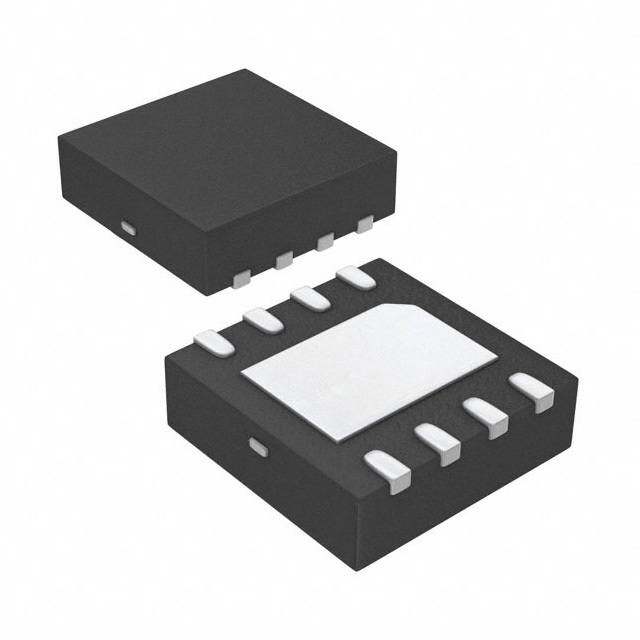
| 产品图片 |
|
| 产品型号 | BD2065AFJ-E2 |
| Rds(On) | 80 毫欧 |
| rohs | 无铅 / 符合限制有害物质指令(RoHS)规范要求 |
| 产品系列 | - |
| 产品目录页面 | |
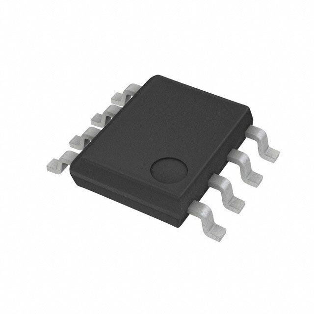
| 供应商器件封装 | 8-SOP-J |
| 其它名称 | BD2065AFJ-E2DKR |
| 内部开关 | 是 |
| 包装 | Digi-Reel® |
| 安装类型 | 表面贴装 |
| 导通电阻 | 80 毫欧 |
| 封装/外壳 | 8-SOIC(0.154",3.90mm 宽) |
| 工作温度 | -40°C ~ 85°C |
| 标准包装 | 1 |
| 特色产品 | http://www.digikey.com/cn/zh/ph/ROHM/highsideswitch.html |
| 电压-电源 | 2.7 V ~ 5.5 V |
| 电压-输入 | 2.7 V ~ 5.5 V |
| 电流-峰值输出 | 1.5A |
| 电流-输出/通道 | 1A |
| 电流限制 | 1.5A |
| 类型 | USB 开关 |
| 输入类型 | 非反相 |
| 输出数 | 1 |


- 商务部:美国ITC正式对集成电路等产品启动337调查
- 曝三星4nm工艺存在良率问题 高通将骁龙8 Gen1或转产台积电
- 太阳诱电将投资9.5亿元在常州建新厂生产MLCC 预计2023年完工
- 英特尔发布欧洲新工厂建设计划 深化IDM 2.0 战略
- 台积电先进制程称霸业界 有大客户加持明年业绩稳了
- 达到5530亿美元!SIA预计今年全球半导体销售额将创下新高
- 英特尔拟将自动驾驶子公司Mobileye上市 估值或超500亿美元
- 三星加码芯片和SET,合并消费电子和移动部门,撤换高东真等 CEO
- 三星电子宣布重大人事变动 还合并消费电子和移动部门
- 海关总署:前11个月进口集成电路产品价值2.52万亿元 增长14.8%


PDF Datasheet 数据手册内容提取
Datasheet 1ch High Side Switch ICs 1. 5A Current Limit High Side Switch ICs BD2061AFJ BD2065AFJ General Description Key Specifications BD2061AFJ and BD2065AFJ are single channel high Input Voltage Range: 2.7V to 5.5V side switch ICs with over-current protection for ON-Resistance: 80mΩ(Typ) Universal Serial Bus (USB) power supply line. These Continuous Current Load: 1.0A ICs have low ON-Resistance N-Channel power Over-Current Threshold: 1.1A (Min), 2.3A (Max) MOSFETs with low supply current, built-in over-current Standby Current: 0.01μA (Typ) protection circuit, thermal shutdown circuit, under Output Rise Time: 1.2ms(Typ) voltage lockout and soft-start circuit. Operating Temperature Range: -40°C to +85°C Features Package W(Typ) D(Typ) H (Max) Built-In Low ON-Resistance Nch MOSFET ( Typ=80mΩ ) Control Input Logic Active-Low: BD2061AFJ Active-High: BD2065AFJ Soft-Start Circuit Over-Current Protection Thermal Shutdown Under Voltage Lockout Function Open Drain Error Flag Output SOP-J8 Reverse-Current Protection when Switch Off Flag Output Delay 4.90mm x 6.00mm x 1.65mm Applications USB Hub in Consumer Appliances, PC, PC Peripheral Equipment, and so forth Typical Application Circuit 5V(Typ) GND OUT VBUS C IN IN OUT + D+ IN OUT C L - D - EN( /EN ) /OC GND Lineup Over-Current Threshold Control Input Package Orderable Part Number Min Typ Max Logic 1.1A 1.5A 2.3A Low SOP-J8 Reel of 2500 BD2061AFJ-E2 1.1A 1.5A 2.3A High SOP-J8 Reel of 2500 BD2065AFJ-E2 ○Product structure:Silicon monolithic integrated circuit ○This product has not designed protection against radioactive rays w ww.rohm.com TSZ02201-0E3E0H300150-1-2 © 2013 ROHM Co., Ltd. All rights reserved. 1/22 TSZ22111・14・001 21.Aug.2014 Rev.003
BD2061AFJ BD2065AFJ Datasheet Block Diagram GND OUT IN UVLO Charge OCD OUT pump IN Gate logic OUT EN(/EN) TSD /OC Pin Configurations BD2061AFJ BD2065AFJ TOP VIEW TOP VIEW 1 GND OUT 8 1 GND OUT 8 2 IN OUT 7 2 IN OUT 7 3 IN OUT 6 3 IN OUT 6 4 /EN /OC 5 4 EN /OC 5 Pin Description Pin No. Symbol I / O Pin Function 1 GND I Ground. Power supply input. 2, 3 IN I Input terminal to the power switch and power supply input terminal of the internal circuit. When used, connect each pin outside. Enable input. /EN: Power switch on at low level. (BD2061AFJ) 4 EN, /EN I EN: Power switch on at high level. (BD2065AFJ) High level input > 2.0V, low level input < 0.8V. Error flag output. 5 /OC O Low at over current, thermal shutdown. Open drain output. Power switch output. 6, 7, 8 OUT O When used, connect each pin outside. www.rohm.com TSZ02201-0E3E0H300150-1-2 © 2013 ROHM Co., Ltd. All rights reserved. 2/22 TSZ22111・15・001 21.Aug.2014 Rev.003
BD2061AFJ BD2065AFJ Datasheet Absolute Maximum Ratings Parameter Symbol Rating Unit Supply Voltage VIN -0.3 to +6.0 V Enable Voltage VEN, V/EN -0.3 to +6.0 V /OC Voltage V/OC -0.3 to +6.0 V /OC Current I/OC 10 mA OUT Voltage VOUT -0.3 to +6.0 V Storage Temperature Tstg -55 to +150 °C Power Dissipation Pd 0.67 (Note 1) W (Note 1) Derating in done 5.4 mW/°C for operating above Ta≧25°C (Mount on 1-layer 70.0mm x 70.0mm x 1.6mm board) Caution: Operating the IC over the absolute maximum ratings may damage the IC. The damage can either be a short circuit between pins or an open circuit between pins and the internal circuitry. Therefore, it is important to consider circuit protection measures, such as adding a fuse, in case the IC is operated over the absolute maximum ratings. Recommended Operating Conditions Rating Parameter Symbol Unit Min Typ Max Operating Voltage VIN 2.7 - 5.5 V Operating Temperature Topr -40 - +85 °C Continuous Output Current ILO 0 - 1.0 A Electrical Characteristics BD2061AFJ (Unless otherwise specified, VIN = 5.0V, Ta = 25°C) Limit Parameter Symbol Unit Conditions Min Typ Max Operating Current IDD - 90 120 μA V/EN = 0V, OUT = OPEN Standby Current ISTB - 0.01 1 μA V/EN = 5V, OUT = OPEN V/ENH 2.0 - - V High Input /EN Input Voltage - - 0.8 V Low Input V/ENL - - 0.4 V Low Input 2.7V≤ VIN ≤4.5V /EN Input Current I/EN -1.0 +0.01 +1.0 μA V/EN = 0V or V/EN = 5V /OC Output Low Voltage V/OC - - 0.5 V I/OC = 5mA /OC Output Leak Current IL/OC - 0.01 1 μA V/OC = 5V /OC Delay Time t/OC - 2.5 8 ms ON-Resistance RON - 80 100 mΩ IOUT = 1.0A Over-Current Threshold ITH 1.1 1.5 2.3 A VIN = 5V, VOUT = 0V, Output Current at Short ISC 1.1 1.5 1.9 A CL = 100μF (RMS) Output Rise Time tON1 - 1.2 10 ms Output Turn ON Time tON2 - 1.5 20 ms RL = 10Ω , CL = OPEN Output Fall Time tOFF1 - 1 20 μs Output Turn OFF Time tOFF2 - 3 40 μs VTUVH 2.1 2.3 2.5 V Increasing VIN UVLO Threshold VTUVL 2.0 2.2 2.4 V Decreasing VIN www.rohm.com TSZ02201-0E3E0H300150-1-2 © 2013 ROHM Co., Ltd. All rights reserved. 3/22 TSZ22111・15・001 21.Aug.2014 Rev.003
BD2061AFJ BD2065AFJ Datasheet Electrical Characteristics - continued BD2065AFJ (Unless otherwise specified, VIN = 5.0V, Ta = 25°C) Limit Parameter Symbol Unit Conditions Min Typ Max Operating Current IDD - 90 120 μA VEN = 5V, OUT = OPEN Standby Current ISTB - 0.01 1 μA VEN = 0V, OUT = OPEN VENH 2.0 - - V High Input EN Input Voltage - - 0.8 V Low Input VENL - - 0.4 V Low Input 2.7V≤ VIN ≤4.5V EN Input Current IEN -1.0 +0.01 +1.0 μA VEN = 0V or VEN = 5V /OC Output Low Voltage V/OC - - 0.5 V I/OC = 5mA /OC Output Leak Current IL/OC - 0.01 1 μA V/OC = 5V /OC Delay Time t/OC - 2.5 8 ms ON-Resistance RON - 80 100 mΩ IOUT = 1.0A Over-Current Threshold ITH 1.1 1.5 2.3 A Output Current at Short ISC 1.1 1.5 1.9 A VCILN == 150V0, μVFO (URT M=S 0)V , Output Rise Time tON1 - 1.2 10 ms Output Turn ON Time tON2 - 1.5 20 ms RL = 10Ω , CL = OPEN Output Fall Time tOFF1 - 1 20 μs Output Turn OFF Time tOFF2 - 3 40 μs VTUVH 2.1 2.3 2.5 V Increasing VIN UVLO Threshold VTUVL 2.0 2.2 2.4 V Decreasing VIN www.rohm.com TSZ02201-0E3E0H300150-1-2 © 2013 ROHM Co., Ltd. All rights reserved. 4/22 TSZ22111・15・001 21.Aug.2014 Rev.003
BD2061AFJ BD2065AFJ Datasheet Measurement Circuit VIN A VIN 1uF 1uF GND OUT GND OUT IN OUT IN OUT IN OUT IN OUT EN(/EN) /OC EN(/EN) /OC RL CL VEN(V/EN) VEN(V/EN) A. Operating Current B. EN, /EN Input Voltage, Output Rise / Fall Time VIN VIN VIN VIN 1uF 10k 1uF I/OC GND OUT GND OUT IN OUT IN OUT IN OUT IN OUT EN(/EN) /OC IOUT CL EN(/EN) /OC VEN(V/EN) VEN(V/EN) C. ON-Resistance, Over Current Detection D. /OC Output Low Voltage Figure 1. Measurement Circuit Timing Diagram tOFF1 tOFF1 tON1 tON1 90% 90% 90% 90% VOUT VOUT 10% 10% 10% 10% tOFF2 tOFF2 tON2 tON2 V/EN VEN V/ENL V/ENH VENH VENL Figure 2. Timing Diagram(BD2061AFJ) Figure 3. Timing Diagram (BD2065AFJ) www.rohm.com TSZ02201-0E3E0H300150-1-2 © 2013 ROHM Co., Ltd. All rights reserved. 5/22 TSZ22111・15・001 21.Aug.2014 Rev.003
BD2061AFJ BD2065AFJ Datasheet Typical Performance Curves 120 120 Ta=25°C VIN=5.0V 100 100 A] A] µ µ [DD 80 [DD 80 ent: I ent: I urr 60 urr 60 C C g g n n ati 40 ati 40 er er p p O O 20 20 0 0 -50 0 50 100 2 3 4 5 6 SUSPuPpLpYly V VOoLltTagAeG: EV I:N V [VIN][ V] Ambient Temperature: Ta [°C] Figure 4. Operating Current vs Supply Voltage Figure 5. Operating current vs Ambient Temperature (EN, /EN Enable) (EN, /EN Enable) 1.0 1.0 Ta=25°C VIN=5.0V T :µA] 0.8 T :µA] 0.8 DBY CURRENby Current: I[STB I[μA]STB00..46 DBY CURRENby Current: I[STB I[μA]STB00..46 Nd Nd STAStan 0.2 STAStan 0.2 0.0 0.0 2 3 4 5 6 -50 0 50 100 SUPSPupLpYl yV VOoLltTaAgGe:E V :I NV [INV[]V ] AMABmIEbNieTn tT TEeMmPpEerRaAtuTreU: RTaE [:° CTa] [℃] Figure 6. Standby Current vs Supply Voltage Figure 7. Standby Current vs Ambient Temperature (EN, /EN Disable) (EN, /EN Disable) www.rohm.com TSZ02201-0E3E0H300150-1-2 © 2013 ROHM Co., Ltd. All rights reserved. 6/22 TSZ22111・15・001 21.Aug.2014 Rev.003
BD2061AFJ BD2065AFJ Datasheet Typical Performance Curves - continued 2.0 2.0 ] V V] Ta=25°C [N VIN=5.0V AGE :,V[N /EN 1.5 VV/EN, E 1.5 Low to High VOLTe: VEV] 0 Low to High ge : High to Low UT oltagV[/EN1.0 High to Low olta 1.0 E INPput VVEN, put V NABLable In 0.5 ble In 0.5 En a E n E 0.0 0.0 2 3 4 5 6 -50 0 50 100 SUSuPpPpLlyY VVoOltLaTgeA:G VEIN : [VVI]N [V] Ambient Temperature : Ta[°C] Figure 8. EN, /EN Input Voltage vs Supply Voltage Figure 9. EN, /EN Input Voltage vs Ambient Temperature 0.5 0.5 GE :[V] C 0.4 Ta=25°C GE :[V] C 0.4 VIN=5.0V W VOLTAoltage: V/OV]0.3 W VOLTAoltage: V/OV]0.3 PUT LOut Low VV[/OC0.2 PUT LOut Low VV[/OC 0.2 UTutp UTutp OO OO OC OC 0.1 OC OC 0.1 // // 0.0 0.0 -50 0 50 100 2 3 4 5 6 SUPSPuLpYp VlyO VLoTltAagGeE: V: VINI N[[VV]] AMABmIEbNieTn Tt TEeMmPpEeRraAtuTreU:R TaE [:° TCa] [℃] Figure 10. /OC Output Low Voltage vs Figure 11. /OC Output Low Voltage vs Supply Voltage Ambient Temperature www.rohm.com TSZ02201-0E3E0H300150-1-2 © 2013 ROHM Co., Ltd. All rights reserved. 7/22 TSZ22111・15・001 21.Aug.2014 Rev.003
BD2061AFJ BD2065AFJ Datasheet Typical Performance Curves - continued 200 200 Ta=25°C VIN=5.0V CE : [mΩ] ON 150 [mΩ] ON 150 NR R RESISTAesistance: mΩ]RON[100 esistance: 1 00 N R R ON- N- O 50 O 50 0 0 2 3 4 5 6 -50 0 50 100 SUPSPuLppYl yV VOoLltaTgAeG: EVI N: [VVD] D[V] Ambient Temperature: Ta [°C] Figure 12. ON-Resistance vs Supply Voltage Figure 13. ON-Resistance vs Ambient Temperature 5.0 5.0 Ta=25°C VIN=5.0V 4.0 4.0 s] s] m m C DELAY TIME : C Delay Time: t[/OC TD[mS] /OC 23..00 C DELAY TIME : TD[mS] /OCC Delay Time: t[/OC 23..00 OO O O // 1.0 / / 1.0 0.0 0.0 2 3 4 5 6 -50 0 50 100 SUPSPupLYpl yV OVoLlTtaAgGeE: :V VINI N[V[V] ] AMABmIEbiNenTt TTEemMpPeErRatAuTreU: RTEa :[ °TCa][ ℃] Figure 14. /OC Delay Time vs Supply Voltage Figure 15. /OC Delay Time vs Ambient Temperature www.rohm.com TSZ02201-0E3E0H300150-1-2 © 2013 ROHM Co., Ltd. All rights reserved. 8/22 TSZ22111・15・001 21.Aug.2014 Rev.003
BD2061AFJ BD2065AFJ Datasheet Typical Performance Curves - continued 2.0 2.0 Ta=25°C VIN=5.0V A] A] Current: I[SC 11..05 Current: I[SC 11..05 Circuit Circuit Short 0.5 Short 0.5 0.0 0.0 2 3 4 5 6 -50 0 50 100 Supply Voltage: VIN [V] Ambient Temperature: Ta [°C] Figure 16. Short Circuit Current Figure 17. Short Circuit Current vs Supply Voltage vs Ambient Temperature 5.0 5.0 Ta=25°C VIN=5.0V s] 4.0 s] 4.0 m m [N1 [N1 O O e: t 3.0 E :e: ts]3.0 m Mmm Ti TITi[1 e E e ON ut Ris 2.0 RISut RisT2.0 p p ut ut O 1.0 O 1.0 0.0 0.0 2 3 4 5 6 -50 0 50 100 Supply Voltage: VIN [V] AMBAImEbNieTn Tt ETeMmPpEeRraAtuTrUe:R TEa :[ °TCa][ ℃] Figure 18. Output Rise Time vs Figure 19. Output Rise Time vs Supply Voltage Ambient Temperature www.rohm.com TSZ02201-0E3E0H300150-1-2 © 2013 ROHM Co., Ltd. All rights reserved. 9/22 TSZ22111・15・001 21.Aug.2014 Rev.003
BD2061AFJ BD2065AFJ Datasheet Typical Performance Curves - continued 5.0 5.0 Ta=25°C VIN=5.0V ms] 4.0 ms] 4.0 [2 [2 N N O O e: t 3.0 e: t 3.0 m m Ti Ti N N O O n 2.0 n 2.0 r r u u T T ut ut p p 1.0 ut 1.0 ut O O 0.0 0.0 -50 0 50 100 2 3 4 5 6 Supply Voltage: VIN [V] Ambient Temperature: Ta [°C] Figure 20. Output Turn ON Time vs Figure 21. Output Turn ON Time vs Supply Voltage Ambient Temperature 5.0 5.0 Ta=25°C VIN=5.0V Output Fall Time: t[µs] OFF1 1234....0000 FALL TIME :Output Fall Time: t[µs] OFF1 T[μs]OFF11234....0000 0.0 0.0 -50 0 50 100 2 3 4 5 6 AMBAImENbiTen Tt ETeMmPpEeRraAtuTrUe:R TEa [:° CTa] [℃] Supply Voltage: VIN [V] Figure 22. Output Fall Time vs Figure 23. Output Fall Time vs Supply Voltage Ambient Temperature www.rohm.com TSZ02201-0E3E0H300150-1-2 © 2013 ROHM Co., Ltd. All rights reserved. 10/22 TSZ22111・15・001 21.Aug.2014 Rev.003
BD2061AFJ BD2065AFJ Datasheet Typical Performance Curves - continued 5.0 5.0 TURN OFF TIME :put Turn OFF Time : t[] µsOFF2T[μs]OFF2 1234....0000 T a=25°C TURN OFF TIME :put Turn OFF Time : t[] µsOFF2T[μs]OFF2 1234....0000 VIN=5.0V Out Out 0.0 0.0 2 3 4 5 6 -50 0 50 100 SSUupPpPlLyY V VoOltaLgTeA G; VE I:N V[VIN][ V] AAMmBbIEieNnTt TTEemMPpeErRaAtuTrUe R; ET a: [T°Ca[℃] ] Figure 24. Output Turn OFF Time Figure 25. Output Turn OFF Time vs Supply Voltage vs Ambient Temperature 2.5 1.0 LO THRESHOLD VOLTAGE :LO Threshold : VV [V] UVLOH, UVLOLV, V[V]UVLOHUVLOL2222....1234 VVUUVVLLOOHL YSTERESIS VOLTAGE : VHYS[VO Hysteresis Voltage : V[] VHYS 0000....2468 VV HL UU O V 2.0 VLU 0.0 U -50 0 50 100 -50 0 50 100 AAmMbBiIeEnNtT T TeEmMpPeEraRtuArTeU ;R TEa :[ °TCa][℃ ] AAMmBbIEieNnTt TTEemMPpEeRraAtuTUreR ;E T :a T[°aC[℃] ] Figure 26. UVLO Threshold Voltage Figure 27. UVLO Hysteresis Voltage vs Ambient Temperature vs Ambient Temperature www.rohm.com TSZ02201-0E3E0H300150-1-2 © 2013 ROHM Co., Ltd. All rights reserved. 11/22 TSZ22111・15・001 21.Aug.2014 Rev.003
BD2061AFJ BD2065AFJ Datasheet Typical Wave Forms V/EN V/EN (5V/div.) (5V/div.) V/OC V/OC (5V/div.) (5V/div.) VOUT (5V/div.) VOUT (5V/div.) VIN=5V IOUT IOUT RL=10Ω (0.5A/div.) (0.5A/div.) VIN=5V CL=100μF RL=10Ω CL=100μF TIME(1ms/div.) TIME(1ms/div.) Figure 28. Output Rise Characteristic Figure 29. Output Fall Characteristic (BD2061AFJ) (BD2061AFJ) V/EN V/OC (5V/div.) (5V/div.) V/OC VOUT (5V/div.) (5V/div.) CL=220μF CL=330μF I(0O.U5TA /div.) CL=147μF IOUT (1.0A/div.) CL=47μF VIN=5V RL= 5Ω VIN=5V TIME (0.5ms/div.) TIME (20ms/div.) Figure 30. Inrush Current Response Figure 31. Over Current Response (BD2061AFJ) Ramped Load (BD2061AFJ) www.rohm.com TSZ02201-0E3E0H300150-1-2 © 2013 ROHM Co., Ltd. All rights reserved. 12/22 TSZ22111・15・001 21.Aug.2014 Rev.003
BD2061AFJ BD2065AFJ Datasheet Typical Wave Forms - continued V/OC V/EN (5V/div.) (5V/div.) V/OC VOUT (5V/div.) (5V/div.) VOUT (5V/div.) IOUT IOUT (1.0A/div.) (1.0A/div.) VIN=5V VIN=5V CL=100μF TIME (2ms/div.) TIME (2ms/div.) Figure 32. Over Current Response Figure 33. Over Current Response Ramped Load Enable to Shortcircuit (BD2061AFJ) (BD2061AFJ) V/OC V/OC (5V/div.) (5V/div.) VOUT VOUT (5V/div.) (5V/div.) Thermal Shutdown VIN=5V CL=100μF IOUT IOUT (1.0A/div.) (1.0A/div.) VIN=5V CL=100μF TIME (2ms/div.) TIME (0.2s/div.) Figure 34. Over Current Response Figure 35. Over Current Response Output 1Ω short at Enable Output 1Ω short at Enable (BD2061AFJ) (BD2061AFJ) www.rohm.com TSZ02201-0E3E0H300150-1-2 © 2013 ROHM Co., Ltd. All rights reserved. 13/22 TSZ22111・15・001 21.Aug.2014 Rev.003
BD2061AFJ BD2065AFJ Datasheet Typical Wave Forms - continued VIN VIN (5V/div.) (5V/div.) VOUT (5V/div.) VOUT (5V/div.) IOUT (1.0A/div.) IOUT (1.0A/div.) V/OC (5V/div.) V/OC (5V/div.) RL=5Ω RL=5Ω TIME (10ms/div.) TIME (10ms/div.) Figure 36. UVLO Response Figure 37. UVLO Response Increasing VIN Decreasing VIN (BD2061AFJ) (BD2061AFJ) Regarding the output rise/fall and over current detection characteristics of BD2065AFJ, refer to the characteristic of BD2061AFJ. www.rohm.com TSZ02201-0E3E0H300150-1-2 © 2013 ROHM Co., Ltd. All rights reserved. 14/22 TSZ22111・15・001 21.Aug.2014 Rev.003
BD2061AFJ BD2065AFJ Datasheet Typical Application Circuit 5V(Typ) VBUS IN Regulator D+ OUT D- GND 10k to GND OUT VBUS 100kΩ USB CIN IN OUT + D+ Controller IN OUT CL - D- EN(/EN) /OC GND Application Information When excessive current flows due to output short circuit or so, ringing occurs by inductance of power source line and IC. This may cause bad effects on IC operations. In order to avoid this case, a bypass capacitor should be connected across the IN terminal and GND terminal of IC. A 1μF or higher value is recommended. Pull-up /OC output by resistance 10kΩ to 100kΩ. Set-up values for CL which satisfies the application. This application circuit does not guarantee its operation. When using the circuit with changes to the external circuit constants, it is better to have an adequate margin for the external components such as static and transient characteristics as well as dispersion of the IC. Functional Description 1. Switch Operation IN terminal and OUT terminal are connected to the drain and the source of switch MOSFET respectively. The IN terminal is also used as power source input to internal control circuit. When the switch is turned ON by EN(/EN) control input, both the IN and OUT terminals are connected by a 80mΩ bidirectional switch. Therefore, current flows from OUT terminal to IN terminal since the flow of current is from higher to lower potentials. On the other hand, when the switch is turned OFF, it is possible to prevent current from flowing reversely from OUT to IN since a parasitic diode between the drain and the source of switch MOSFET is not present. 2. Thermal Shutdown Circuit (TSD) If over-current would continue, the temperature of the IC would increase drastically. If the junction temperature goes beyond 140°C (Typ) during the condition of over-current detection, thermal shutdown circuit operates and turns the power switch OFF, causing the IC to output an error flag (/OC). Then, when the junction temperature drops lower than 120°C (Typ), the power switch is turned ON and error flag (/OC) is cancelled. This operation repeats unless the cause of the increase of chip’s temperature is removed or the output of power switch is turned OFF. The thermal shutdown circuit operates when the switch is ON (EN(/EN) signal is active). www.rohm.com TSZ02201-0E3E0H300150-1-2 © 2013 ROHM Co., Ltd. All rights reserved. 15/22 TSZ22111・15・001 21.Aug.2014 Rev.003
BD2061AFJ BD2065AFJ Datasheet 3. Over-Current Detection (OCD) The over-current detection circuit limits current (ISC) and outputs error flag (/OC) when current flowing in each switch MOSFET exceeds a specified value. The over-current detection circuit works when the switch is ON (EN(/EN) signal is active). There are three types of response against over-current: (1) When the switch is turned on while the output is in short circuit status, the switch goes into current limit status immediately. (2) When the output short circuits or high-current load is connected while the switch is ON, very large current flows until the over-current limit circuit reacts. When it exceeds the detection value, current limitation is carried out. (3) When the output current increases gradually, current limit circuit would not operate unless the output current exceeds the over-current detection value. But when the output current increases gradually and it exceeds the detection value, current limitation is carried out. 4. Under Voltage Lockout (UVLO) UVLO circuit prevents the switch from turning on until VIN exceeds 2.3V(Typ). If VIN drops below 2.2V(Typ) while the switch is ON, then UVLO shuts off the power switch. UVLO has hysteresis of a 100mV(Typ). Under voltage lockout circuit works when the switch is on (EN(/EN) signal is active). 5. Error Flag (/OC) Output Error flag output is N-MOS open drain output. During detection of over-current and/or thermal shutdown, the output level is low. Over-current detection has delay filter. This delay filter prevents current detection flags from being sent during instantaneous events such as inrush current at switch on or during hot plug. If fault flag output is unused, /OC pin should be connected to open or ground line. V/EN VOUT Output Short Circuit Thermal Shutdown IOUT V/OC /OC Delay Time Figure 38. Over Current Detection, Thermal Shutdown Timing (BD2061FJ) VEN VOUT Output Short Circuit Thermal Shutdown IOUT V/OC /OC Delay Time Figure 39. Over Current Detection, Thermal Shutdown Timing (BD2065AFJ) www.rohm.com TSZ02201-0E3E0H300150-1-2 © 2013 ROHM Co., Ltd. All rights reserved. 16/22 TSZ22111・15・001 21.Aug.2014 Rev.003
BD2061AFJ BD2065AFJ Datasheet Power Dissipation (SOP-J8) 700 600 W] W] m m P[dPd [500 n :N : oO400 patiATI ssiSIP300 DiS er R DI wE200 oW P O P 100 0 0 25 50 75 100 125 150 AMBIEANmT bTEieMnPt ETReAmTpUeRrEa t:u Trae [:℃ Ta][°C] 70mm x 70mm x 1.6mm Glass Epoxy Board Figure 40. Power Dissipation Curve (Pd-Ta Curve) I/O Equivalence Circuit Symbol Pin No Equivalence Circuit EN(/EN) 4 /OC 5 OUT 6,7,8 www.rohm.com TSZ02201-0E3E0H300150-1-2 © 2013 ROHM Co., Ltd. All rights reserved. 17/22 TSZ22111・15・001 21.Aug.2014 Rev.003
BD2061AFJ BD2065AFJ Datasheet Operational Notes 1. Reverse Connection of Power Supply Connecting the power supply in reverse polarity can damage the IC. Take precautions against reverse polarity when connecting the power supply, such as mounting an external diode between the power supply and the IC’s power supply pins. 2. Power Supply Lines Design the PCB layout pattern to provide low impedance supply lines. Separate the ground and supply lines of the digital and analog blocks to prevent noise in the ground and supply lines of the digital block from affecting the analog block. Furthermore, connect a capacitor to ground at all power supply pins. Consider the effect of temperature and aging on the capacitance value when using electrolytic capacitors. 3. Ground Voltage Ensure that no pins are at a voltage below that of the ground pin at any time, even during transient condition. 4. Ground Wiring Pattern When using both small-signal and large-current ground traces, the two ground traces should be routed separately but connected to a single ground at the reference point of the application board to avoid fluctuations in the small-signal ground caused by large currents. Also ensure that the ground traces of external components do not cause variations on the ground voltage. The ground lines must be as short and thick as possible to reduce line impedance. 5. Thermal Consideration Should by any chance the power dissipation rating be exceeded the rise in temperature of the chip may result in deterioration of the properties of the chip. The absolute maximum rating of the Pd stated in this specification is when the IC is mounted on a 70mm x 70mm x 1.6mm glass epoxy board. In case of exceeding this absolute maximum rating, increase the board size and copper area to prevent exceeding the Pd rating. 6. Recommended Operating Conditions These conditions represent a range within which the expected characteristics of the IC can be approximately obtained. The electrical characteristics are guaranteed under the conditions of each parameter. 7. In rush Current When power is first supplied to the IC, it is possible that the internal logic may be unstable and inrush current may flow instantaneously due to the internal powering sequence and delays, especially if the IC has more than one power supply. Therefore, give special consideration to power coupling capacitance, power wiring, width of ground wiring, and routing of connections. 8. Operation Under Strong Electromagnetic Field Operating the IC in the presence of a strong electromagnetic field may cause the IC to malfunction. 9. Testing on Application Boards When testing the IC on an application board, connecting a capacitor directly to a low-impedance output pin may subject the IC to stress. Always discharge capacitors completely after each process or step. The IC’s power supply should always be turned off completely before connecting or removing it from the test setup during the inspection process. To prevent damage from static discharge, ground the IC during assembly and use similar precautions during transport and storage. 10. Inter-pin Short and Mounting Errors Ensure that the direction and position are correct when mounting the IC on the PCB. Incorrect mounting may result in damaging the IC. Avoid nearby pins being shorted to each other especially to ground, power supply and output pin. Inter-pin shorts could be due to many reasons such as metal particles, water droplets (in very humid environment) and unintentional solder bridge deposited in between pins during assembly to name a few. www.rohm.com TSZ02201-0E3E0H300150-1-2 © 2013 ROHM Co., Ltd. All rights reserved. 18/22 TSZ22111・15・001 21.Aug.2014 Rev.003
BD2061AFJ BD2065AFJ Datasheet Operational Notes - continued 11. Unused Input Pins Input pins of an IC are often connected to the gate of a MOS transistor. The gate has extremely high impedance and extremely low capacitance. If left unconnected, the electric field from the outside can easily charge it. The small charge acquired in this way is enough to produce a significant effect on the conduction through the transistor and cause unexpected operation of the IC. So unless otherwise specified, unused input pins should be connected to the power supply or ground line. 12. Regarding the Input Pin of the IC This monolithic IC contains P+ isolation and P substrate layers between adjacent elements in order to keep them isolated. P-N junctions are formed at the intersection of the P layers with the N layers of other elements, creating a parasitic diode or transistor. For example (refer to figure below): When GND > Pin A and GND > Pin B, the P-N junction operates as a parasitic diode. When GND > Pin B, the P-N junction operates as a parasitic transistor. Parasitic diodes inevitably occur in the structure of the IC. The operation of parasitic diodes can result in mutual interference among circuits, operational faults, or physical damage. Therefore, conditions that cause these diodes to operate, such as applying a voltage lower than the GND voltage to an input pin (and thus to the P substrate) should be avoided. Resistor Transistor (NPN) Pin A Pin B B Pin B C Pin A E P+ P P+ P+ N P P+ B C N N N N Parasitic N N N E Elements Parasitic P Substrate P Substrate Elements GND GND GND GND Parasitic Parasitic N Region Elements Elements close-by Figure 41. Example of monolithic IC structure 13. Ceramic Capacitor When using a ceramic capacitor, determine the dielectric constant considering the change of capacitance with temperature and the decrease in nominal capacitance due to DC bias and others. 14. Thermal Shutdown Circuit(TSD) This IC has a built-in thermal shutdown circuit that prevents heat damage to the IC. Normal operation should always be within the IC’s power dissipation rating. If however the rating is exceeded for a continued period, the junction temperature (Tj) will rise which will activate the TSD circuit that will turn OFF all output pins. When the Tj falls below the TSD threshold, the circuits are automatically restored to normal operation. Note that the TSD circuit operates in a situation that exceeds the absolute maximum ratings and therefore, under no circumstances, should the TSD circuit be used in a set design or for any purpose other than protecting the IC from heat damage. 15. Thermal design Perform thermal design in which there are adequate margins by taking into account the power dissipation (Pd) in actual states of use. www.rohm.com TSZ02201-0E3E0H300150-1-2 © 2013 ROHM Co., Ltd. All rights reserved. 19/22 TSZ22111・15・001 21.Aug.2014 Rev.003
BD2061AFJ BD2065AFJ Datasheet Ordering Information B D 2 0 6 1 A F J - E 2 Part Number Package Packaging and forming specification FJ: SOP-J8 E2: Embossed tape and reel B D 2 0 6 5 A F J - E 2 Part Number Package Packaging and forming specification FJ: SOP-J8 E2: Embossed tape and reel Marking Diagram SOP-J8 (TOP VIEW) Part Number Marking LOT Number 1PIN MARK Part Number Part Number Marking BD2061AFJ D061A BD2065AFJ D065A www.rohm.com TSZ02201-0E3E0H300150-1-2 © 2013 ROHM Co., Ltd. All rights reserved. 20/22 TSZ22111・15・001 21.Aug.2014 Rev.003
BD2061AFJ BD2065AFJ Datasheet Physical Dimension, Tape and Reel Information Package Name SOP-J8 www.rohm.com TSZ02201-0E3E0H300150-1-2 © 2013 ROHM Co., Ltd. All rights reserved. 21/22 TSZ22111・15・001 21.Aug.2014 Rev.003
BD2061AFJ BD2065AFJ Datasheet Revision History Date Revision Changes 11.Mar.2013 001 New Release Changed character color from RED to BLOCK of figure 41. 25.Jun.2013 002 Modified Block Diagram and Marking Diagram. 21.Aug.2014 003 Applied the ROHM Standard Style and improved understandability. www.rohm.com TSZ02201-0E3E0H300150-1-2 © 2013 ROHM Co., Ltd. All rights reserved. 22/22 TSZ22111・15・001 21.Aug.2014 Rev.003
DDaattaasshheeeett Notice Precaution on using ROHM Products 1. Our Products are designed and manufactured for application in ordinary electronic equipments (such as AV equipment, OA equipment, telecommunication equipment, home electronic appliances, amusement equipment, etc.). If you intend to use our Products in devices requiring extremely high reliability (such as medical equipment (Note 1), transport equipment, traffic equipment, aircraft/spacecraft, nuclear power controllers, fuel controllers, car equipment including car accessories, safety devices, etc.) and whose malfunction or failure may cause loss of human life, bodily injury or serious damage to property (“Specific Applications”), please consult with the ROHM sales representative in advance. Unless otherwise agreed in writing by ROHM in advance, ROHM shall not be in any way responsible or liable for any damages, expenses or losses incurred by you or third parties arising from the use of any ROHM’s Products for Specific Applications. (Note1) Medical Equipment Classification of the Specific Applications JAPAN USA EU CHINA CLASSⅢ CLASSⅡb CLASSⅢ CLASSⅢ CLASSⅣ CLASSⅢ 2. ROHM designs and manufactures its Products subject to strict quality control system. However, semiconductor products can fail or malfunction at a certain rate. Please be sure to implement, at your own responsibilities, adequate safety measures including but not limited to fail-safe design against the physical injury, damage to any property, which a failure or malfunction of our Products may cause. The following are examples of safety measures: [a] Installation of protection circuits or other protective devices to improve system safety [b] Installation of redundant circuits to reduce the impact of single or multiple circuit failure 3. Our Products are designed and manufactured for use under standard conditions and not under any special or extraordinary environments or conditions, as exemplified below. Accordingly, ROHM shall not be in any way responsible or liable for any damages, expenses or losses arising from the use of any ROHM’s Products under any special or extraordinary environments or conditions. If you intend to use our Products under any special or extraordinary environments or conditions (as exemplified below), your independent verification and confirmation of product performance, reliability, etc, prior to use, must be necessary: [a] Use of our Products in any types of liquid, including water, oils, chemicals, and organic solvents [b] Use of our Products outdoors or in places where the Products are exposed to direct sunlight or dust [c] Use of our Products in places where the Products are exposed to sea wind or corrosive gases, including Cl2, H2S, NH3, SO2, and NO2 [d] Use of our Products in places where the Products are exposed to static electricity or electromagnetic waves [e] Use of our Products in proximity to heat-producing components, plastic cords, or other flammable items [f] Sealing or coating our Products with resin or other coating materials [g] Use of our Products without cleaning residue of flux (even if you use no-clean type fluxes, cleaning residue of flux is recommended); or Washing our Products by using water or water-soluble cleaning agents for cleaning residue after soldering [h] Use of the Products in places subject to dew condensation 4. The Products are not subject to radiation-proof design. 5. Please verify and confirm characteristics of the final or mounted products in using the Products. 6. In particular, if a transient load (a large amount of load applied in a short period of time, such as pulse. is applied, confirmation of performance characteristics after on-board mounting is strongly recommended. Avoid applying power exceeding normal rated power; exceeding the power rating under steady-state loading condition may negatively affect product performance and reliability. 7. De-rate Power Dissipation (Pd) depending on Ambient temperature (Ta). When used in sealed area, confirm the actual ambient temperature. 8. Confirm that operation temperature is within the specified range described in the product specification. 9. ROHM shall not be in any way responsible or liable for failure induced under deviant condition from what is defined in this document. Precaution for Mounting / Circuit board design 1. When a highly active halogenous (chlorine, bromine, etc.) flux is used, the residue of flux may negatively affect product performance and reliability. 2. In principle, the reflow soldering method must be used; if flow soldering method is preferred, please consult with the ROHM representative in advance. For details, please refer to ROHM Mounting specification Notice – GE Rev.002 © 2013 ROHM Co., Ltd. All rights reserved.
DDaattaasshheeeett Precautions Regarding Application Examples and External Circuits 1. If change is made to the constant of an external circuit, please allow a sufficient margin considering variations of the characteristics of the Products and external components, including transient characteristics, as well as static characteristics. 2. You agree that application notes, reference designs, and associated data and information contained in this document are presented only as guidance for Products use. Therefore, in case you use such information, you are solely responsible for it and you must exercise your own independent verification and judgment in the use of such information contained in this document. ROHM shall not be in any way responsible or liable for any damages, expenses or losses incurred by you or third parties arising from the use of such information. Precaution for Electrostatic This Product is electrostatic sensitive product, which may be damaged due to electrostatic discharge. Please take proper caution in your manufacturing process and storage so that voltage exceeding the Products maximum rating will not be applied to Products. Please take special care under dry condition (e.g. Grounding of human body / equipment / solder iron, isolation from charged objects, setting of Ionizer, friction prevention and temperature / humidity control). Precaution for Storage / Transportation 1. Product performance and soldered connections may deteriorate if the Products are stored in the places where: [a] the Products are exposed to sea winds or corrosive gases, including Cl2, H2S, NH3, SO2, and NO2 [b] the temperature or humidity exceeds those recommended by ROHM [c] the Products are exposed to direct sunshine or condensation [d] the Products are exposed to high Electrostatic 2. Even under ROHM recommended storage condition, solderability of products out of recommended storage time period may be degraded. It is strongly recommended to confirm solderability before using Products of which storage time is exceeding the recommended storage time period. 3. Store / transport cartons in the correct direction, which is indicated on a carton with a symbol. Otherwise bent leads may occur due to excessive stress applied when dropping of a carton. 4. Use Products within the specified time after opening a humidity barrier bag. Baking is required before using Products of which storage time is exceeding the recommended storage time period. Precaution for Product Label QR code printed on ROHM Products label is for ROHM’s internal use only. Precaution for Disposition When disposing Products please dispose them properly using an authorized industry waste company. Precaution for Foreign Exchange and Foreign Trade act Since our Products might fall under controlled goods prescribed by the applicable foreign exchange and foreign trade act, please consult with ROHM representative in case of export. Precaution Regarding Intellectual Property Rights 1. All information and data including but not limited to application example contained in this document is for reference only. ROHM does not warrant that foregoing information or data will not infringe any intellectual property rights or any other rights of any third party regarding such information or data. ROHM shall not be in any way responsible or liable for infringement of any intellectual property rights or other damages arising from use of such information or data.: 2. No license, expressly or implied, is granted hereby under any intellectual property rights or other rights of ROHM or any third parties with respect to the information contained in this document. Other Precaution 1. This document may not be reprinted or reproduced, in whole or in part, without prior written consent of ROHM. 2. The Products may not be disassembled, converted, modified, reproduced or otherwise changed without prior written consent of ROHM. 3. In no event shall you use in any way whatsoever the Products and the related technical information contained in the Products or this document for any military purposes, including but not limited to, the development of mass-destruction weapons. 4. The proper names of companies or products described in this document are trademarks or registered trademarks of ROHM, its affiliated companies or third parties. Notice – GE Rev.002 © 2013 ROHM Co., Ltd. All rights reserved.
DDaattaasshheeeett General Precaution 1. Before you use our Products, you are requested to carefully read this document and fully understand its contents. ROHM shall not be in any way responsible or liable for failure, malfunction or accident arising from the use of a ny ROHM’s Products against warning, caution or note contained in this document. 2. All information contained in this document is current as of the issuing date and subj ect to change without any prior notice. Before purchasing or using ROHM’s Products, please confirm the latest information with a ROHM sale s representative. 3. The information contained in this document is provided on an “as is” basis and ROHM does not warrant that all information contained in this document is accurate an d/or error-free. ROHM shall not be in any way responsible or liable for any damages, expenses or losses incurred by you or third parties resulting from inaccuracy or errors of or concerning such information. Notice – WE Rev.001 © 2014 ROHM Co., Ltd. All rights reserved.
Mouser Electronics Authorized Distributor Click to View Pricing, Inventory, Delivery & Lifecycle Information: R OHM Semiconductor: BD2061AFJ-E2 BD2065AFJ-E2