ICGOO在线商城 > 传感器,变送器 > 温度传感器 - 模拟和数字输出 > TMP422AMDCNTEP

 Datasheet下载
- 型号: TMP422AMDCNTEP
- 制造商: Texas Instruments
- 库位|库存: xxxx|xxxx
- 要求:
| 数量阶梯 | 香港交货 | 国内含税 |
| +xxxx | $xxxx | ¥xxxx |
查看当月历史价格
查看今年历史价格
TMP422AMDCNTEP产品简介:
ICGOO电子元器件商城为您提供TMP422AMDCNTEP由Texas Instruments设计生产,在icgoo商城现货销售,并且可以通过原厂、代理商等渠道进行代购。 TMP422AMDCNTEP价格参考。Texas InstrumentsTMP422AMDCNTEP封装/规格:温度传感器 - 模拟和数字输出, 温度传感器 数字,本地/远程 -40°C ~ 125°C 11 b SOT-23-8。您可以下载TMP422AMDCNTEP参考资料、Datasheet数据手册功能说明书,资料中有TMP422AMDCNTEP 详细功能的应用电路图电压和使用方法及教程。
TMP422AMDCNTEP 是 Texas Instruments(德州仪器)生产的一款高精度数字温度传感器,具有 I²C/SMBus 接口,支持多通道温度监测。该器件主要用于需要高精度、多点温度监控的应用场景,适用于工业、汽车和通信等多个领域。

具体应用场景包括:

1. 服务器与计算机系统:用于监测CPU、GPU、电源模块等关键部件的温度,确保系统在安全温度范围内运行,防止过热损坏。

2. 工业控制系统:如PLC、工业PC和自动化设备中,对电机驱动器、变频器及其他发热元件进行实时温度监控,保障设备稳定运行。

3. 电信与网络设备:应用于基站、交换机、路由器等设备中,监测内部组件温度,实现风扇调速或过温保护功能。

4. 汽车电子系统:如车载信息娱乐系统、电池管理系统(BMS)中,用于监测电子控制单元(ECU)或其他关键模块的温度。

5. 测试与测量设备:用于高精度温度测量仪表中,提供可靠的温度数据采集功能。

该器件采用小型VSSOP封装,适合空间受限的设计,并支持多个传感器在同一总线上工作,便于扩展多点测温系统。其高精度和稳定性使其成为多种精密温度监控应用的理想选择。
| 参数 | 数值 |
| 产品目录 | 集成电路 (IC)热管理产品 |
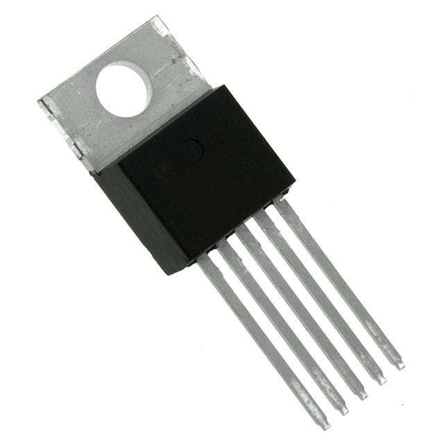
| 描述 | IC TEMP SENS REMOTE/LOCL SOT23-8板上安装温度传感器 Remote and Local Temp Sensor |
| 产品分类 | |
| 品牌 | Texas Instruments |
| 产品手册 | |
| 产品图片 |
|
| rohs | 符合RoHS无铅 / 符合限制有害物质指令(RoHS)规范要求 |
| 产品系列 | 板上安装温度传感器,Texas Instruments TMP422AMDCNTEP- |
| 数据手册 | |
| 产品型号 | TMP422AMDCNTEP |
| 产品种类 | 板上安装温度传感器 |
| 传感器类型 | 内部和外部 |
| 供应商器件封装 | SOT-23-8 |
| 关闭 | Shutdown |
| 其它名称 | 296-29988-6 |
| 准确性 | +/- 1 C |
| 功能 | 温度监控系统(传感器) |
| 包装 | Digi-Reel® |
| 商标 | Texas Instruments |
| 安装类型 | 表面贴装 |
| 安装风格 | SMD/SMT |
| 封装 | Reel |
| 封装/外壳 | SOT-23-8 |
| 封装/箱体 | SOT-23-8 |
| 工作温度 | -55°C ~ 125°C |
| 工厂包装数量 | 250 |
| 感应温度 | -55°C ~ 150°C |
| 拓扑 | ADC,比较器,寄存器库 |
| 数字输出-总线接口 | 2-Wire, I2C, SMBus |
| 最大工作温度 | + 125 C |
| 最小工作温度 | - 55 C |
| 标准包装 | 1 |
| 电压-电源 | 2.7 V ~ 5.5 V |
| 电源电压-最大 | 5.5 V |
| 电源电压-最小 | 2.7 V |
| 电源电流 | 10 mA |
| 精度 | ±2.5°C 本地(最大), ±5°C 远程(最大) |
| 系列 | TMP422-EP |
| 设备功能 | Temperature Sensor |
| 输出报警 | 无 |
| 输出类型 | Digital |
| 输出风扇 | 无 |
| 配置 | Local, Remote |


- 商务部:美国ITC正式对集成电路等产品启动337调查
- 曝三星4nm工艺存在良率问题 高通将骁龙8 Gen1或转产台积电
- 太阳诱电将投资9.5亿元在常州建新厂生产MLCC 预计2023年完工
- 英特尔发布欧洲新工厂建设计划 深化IDM 2.0 战略
- 台积电先进制程称霸业界 有大客户加持明年业绩稳了
- 达到5530亿美元!SIA预计今年全球半导体销售额将创下新高
- 英特尔拟将自动驾驶子公司Mobileye上市 估值或超500亿美元
- 三星加码芯片和SET,合并消费电子和移动部门,撤换高东真等 CEO
- 三星电子宣布重大人事变动 还合并消费电子和移动部门
- 海关总署:前11个月进口集成电路产品价值2.52万亿元 增长14.8%


PDF Datasheet 数据手册内容提取
TMP422-EP www.ti.com SBOS577–SEPTEMBER2011 ±1°C REMOTE TEMPERATURE AND ±2.5°C LOCAL TEMPERATURE SENSOR IN SOT23-8 CheckforSamples:TMP422-EP FEATURES SUPPORTS DEFENSE, AEROSPACE AND 1 MEDICAL APPLICATIONS • SOT23-8Package 234 • ±1°CRemoteDiodeSensor(Max) • ControlledBaseline • ±2.5°CLocalTemperatureSensor(Max) • OneAssembly/TestSite • SeriesResistanceCancellation • OneFabricationSite • n-FactorCorrection • AvailableinMilitary(–55°Cto125°C) TemperatureRange(1) • Two-Wire/SMBus™SerialInterface • ExtendedProductLifeCycle • MultipleInterfaceAddresses • ExtendedProduct-ChangeNotification • DiodeFaultDetection • ProductTraceability • RoHSCompliantandNOSb/Br +5V APPLICATIONS • Processor/FPGATemperatureMonitoring • LCD/DLP®/LCOSProjectors 8 V+ • Servers 1 DX1 SCL 7 SMBus • CentralOfficeTelecomEquipment 2 6 Controller DX2 SDA • StorageAreaNetworks(SAN) 3 DX3 4 DX4 GND 5 1 Channel Local 2 Channels Remote (1) Additionaltemperaturerangesavailable-contactfactory DESCRIPTION The TMP422 is a remote temperature sensor monitor with a built-in local temperature sensor. The remote temperature sensor diode-connected transistors are typically low-cost, NPN- or PNP-type transistors or diodes thatareanintegralpartofmicrocontrollers,microprocessors,orFPGAs. Remote accuracy is ±1°C for multiple IC manufacturers, with no calibration needed. The two-wire serial interface acceptsSMBuswritebyte,readbyte,sendbyte,andreceivebytecommandstoconfigurethedevice. The TMP422 includes series resistance cancellation, programmable non-ideality factor, wide remote temperature measurementrange(upto150°C),anddiodefaultdetection. TheTMP422isavailableinaSOT23-8package. 1 Pleasebeawarethatanimportantnoticeconcerningavailability,standardwarranty,anduseincriticalapplicationsofTexas Instrumentssemiconductorproductsanddisclaimerstheretoappearsattheendofthisdatasheet. DLPisaregisteredtrademarkofTexasInstruments. 2 SMBusisatrademarkofIntelCorporation. 3 Allothertrademarksarethepropertyoftheirrespectiveowners. 4 PRODUCTIONDATAinformationiscurrentasofpublicationdate. Copyright©2011,TexasInstrumentsIncorporated Products conform to specifications per the terms of the Texas Instruments standard warranty. Production processing does not necessarilyincludetestingofallparameters.
TMP422-EP SBOS577–SEPTEMBER2011 www.ti.com This integrated circuit can be damaged by ESD. Texas Instruments recommends that all integrated circuits be handled with appropriateprecautions.Failuretoobserveproperhandlingandinstallationprocedurescancausedamage. ESDdamagecanrangefromsubtleperformancedegradationtocompletedevicefailure.Precisionintegratedcircuitsmaybemore susceptibletodamagebecauseverysmallparametricchangescouldcausethedevicenottomeetitspublishedspecifications. Table1. ORDERINGINFORMATION(1) ORDERABLEPART PACKAGE PACKAGE PRODUCT NUMBER PACKAGE-LEAD DESIGNATOR(2) MARKING VIDNUMBER TMP422 TMP422AMDCNTEP SOT23-8 DCN TMP4 V62/11618-01XE (1) ForthemostcurrentpackageandorderinginformationseethePackageOptionAddendumattheendofthisdocument,orseetheTI websiteatwww.ti.com. (2) Packagedrawings,standardpackingquantities,thermaldata,symbolization,andPCBdesignguidelinesareavailableat www.ti.com/sc/package. ABSOLUTE MAXIMUM RATINGS(1) Overoperatingfree-airtemperaturerange,unlessotherwisenoted. TMP422 UNIT PowerSupply,V +7 V S Pins1,2,3,and4only –0.5toV +0.5 V S InputVoltage Pins6and7only –0.5to7 V InputCurrent 10 mA Powerdissipation,P 230 mW D StorageTemperatureRange –65to+150 °C JunctionTemperature(T max) +150 °C J HumanBodyModel(HBM) 3000 V ESDRating ChargedDeviceModel(CDM) 1000 V MachineModel(MM) 200 V (1) Stressesabovetheseratingsmaycausepermanentdamage.Exposuretoabsolutemaximumconditionsforextendedperiodsmay degradedevicereliability.Thesearestressratingsonly,andfunctionaloperationofthedeviceattheseoranyotherconditionsbeyond thosespecifiedisnotimplied. 2 SubmitDocumentationFeedback Copyright©2011,TexasInstrumentsIncorporated ProductFolderLink(s):TMP422-EP
TMP422-EP www.ti.com SBOS577–SEPTEMBER2011 ELECTRICAL CHARACTERISTICS AtT =–55°Cto+125°CandV =2.7Vto5.5V,unlessotherwisenoted. A S PARAMETER CONDITIONS MIN TYP MAX UNIT TEMPERATUREERROR LocalTemperatureSensor TELOCAL TA=–55°Cto+125°C ±1.25 ±2.5 °C RemoteTemperatureSensor(1) TEREMOTE TA=+15°Cto+85°C,TD=–55°Cto+125°C,VS=3.3V 0.25 ±1 °C TA=–55°Cto+125°C,TD=–55°Cto+125°C,VS=3.3V ±1 ±3 °C TA=–55°Cto+125°C,TD=–55°Cto+125°C ±3 ±5 °C vsSupply(Local/Remote) VS=2.7Vto5.5V ±0.2 ±0.72 °C/V TEMPERATUREMEASUREMENT ConversionTime(perchannel) 100 115 130 ms Resolution LocalTemperatureSensor(programmable) 12 Bits RemoteTemperatureSensor 12 Bits RemoteSensorSourceCurrents High SeriesResistance3kΩMax 120 μA MediumHigh 60 μA MediumLow 12 μA Low 6 μA RemoteTransistorIdealityFactor η OptimizedIdealityFactor 1.008 SMBusINTERFACE LogicInputHighVoltage(SCL,SDA) VIH 2.1 V LogicInputLowVoltage(SCL,SDA) VIL 0.8 V Hysteresis 500 mV SMBusOutputLowSinkCurrent 6 mA SDAOutputLowVoltage VOL IOUT=6mA 0.15 0.4 V LogicInputCurrent 0≤VIN≤6V –1 +1 μA SMBusInputCapacitance(SCL,SDA) 3 pF SMBusClockFrequency 3.4 MHz SMBusTimeout 25 30 35 ms SCLFallingEdgetoSDAValidTime 1 μs DIGITALINPUTS InputCapacitance 3 pF InputLogicLevels InputHighVoltage VIH 0.7(V+) (V+)+0.5 V InputLowVoltage VIL –0.5 0.3(V+) V LeakageInputCurrent IIN 0V≤VIN≤VS 1 μA POWERSUPPLY SpecifiedVoltageRange VS 2.7 5.5 V QuiescentCurrent IQ 0.0625ConversionsperSecond 32 38 μA EightConversionsperSecond 400 525 μA SerialBusInactive,ShutdownMode 3 10 μA SerialBusActive,fS=400kHz,ShutdownMode 90 μA SerialBusActive,fS=3.4MHz,ShutdownMode 350 μA UndervoltageLockout UVLO 2.3 2.4 2.6 V Power-OnResetThreshold POR 1.6 2.3 V TEMPERATURERANGE SpecifiedRange –55 +125 °C ThermalResistance, junction-to-ambientSOT23 θJA 164 °C/W ThermalResistance,junction-to-case SOT23 θJC 108 °C/W (1) Testedwithlessthan5Ωeffectiveseriesresistanceand100pFdifferentialinputcapacitance. Copyright©2011,TexasInstrumentsIncorporated SubmitDocumentationFeedback 3 ProductFolderLink(s):TMP422-EP
TMP422-EP SBOS577–SEPTEMBER2011 www.ti.com PIN CONFIGURATION DCNPACKAGE SOT23-8 (TOPVIEW) DX1 1 8 V+ DX2 2 7 SCL TMP422 DX3 3 6 SDA DX4 4 5 GND PINASSIGNMENTS TMP422 NO. NAME DESCRIPTION 1 DX1 Channel1remotetemperaturesensorconnectionpin.AlsosetstheTMP422address;seeTable10. 2 DX2 Channel1remotetemperaturesensorconnectionpin.AlsosetstheTMP422address;seeTable10. 3 DX3 Channel2remotetemperaturesensorconnectionpin.AlsosetstheTMP422address;seeTable10. 4 DX4 Channel2remotetemperaturesensorconnectionpin.AlsosetstheTMP422address;seeTable10. 5 GND Ground 6 SDA SerialdatalineforSMBus,open-drain;requirespull-upresistortoV+. 7 SCL SerialclocklineforSMBus,open-drain;requirespull-upresistortoV+. 8 V+ Positivesupplyvoltage(2.7Vto5.5V) 4 SubmitDocumentationFeedback Copyright©2011,TexasInstrumentsIncorporated ProductFolderLink(s):TMP422-EP
TMP422-EP www.ti.com SBOS577–SEPTEMBER2011 TYPICAL CHARACTERISTICS AtT =+25°CandV =+5.0V,unlessotherwisenoted. A S REMOTETEMPERATUREERROR LOCALTEMPERATUREERROR vs vs TEMPERATURE TEMPERATURE 3 3 V+ = 3.3V T = +25°C V+ = 3.3V 50 Units Shown °perature Error (C) 210 3h0R= ET M1yO.p0Tic0Ea8l Units Shown °erature Error ()C 210 m p ote Te -1 al Tem -1 em -2 Loc -2 R -3 -3 -50 -25 0 25 50 75 100 125 -50 -25 0 25 50 75 100 125 Ambient Temperature, TA(°C) Ambient Temperature, TA(°C) Figure1. Figure2. REMOTETEMPERATUREERROR REMOTETEMPERATUREERROR vs vs SERIESRESISTANCE LEAKAGERESISTANCE (Diode-ConnectedTransistor,2N3906PNP) 60 2.0 °or (C) 40 °or ()C 11..50 V+ = 2.7V Err 20 Err e R-GND e 0.5 ur ur perat 0 perat 0 V+ = 5.5V Tem -20 R-V+ Tem -0.5 ote ote -1.0 m m e -40 e R R -1.5 -60 -2.0 0 5 10 15 20 25 30 0 500 1000 1500 2000 2500 3000 3500 Leakage Resistance (MW) R (W) S Figure3. Figure4. Copyright©2011,TexasInstrumentsIncorporated SubmitDocumentationFeedback 5 ProductFolderLink(s):TMP422-EP
TMP422-EP SBOS577–SEPTEMBER2011 www.ti.com TYPICAL CHARACTERISTICS (continued) AtT =+25°CandV =+5.0V,unlessotherwisenoted. A S REMOTETEMPERATUREERROR vs REMOTETEMPERATUREERROR SERIESRESISTANCE vs (GNDCollector-ConnectedTransistor,2N3906PNP) DIFFERENTIALCAPACITANCE 2.0 3 °or ()C 11..50 V+ = 2.7V °or (C) 2 Err Err 1 e 0.5 e eratur 0 V+ = 5.5V eratur 0 p p Tem -0.5 Tem -1 ote -1.0 ote m m Re -1.5 Re -2 -2.0 -3 0 500 1000 1500 2000 2500 3000 3500 0 0.5 1.0 1.5 2.0 2.5 3.0 R (W) Capacitance (nF) S Figure5. Figure6. TEMPERATUREERROR QUIESCENTCURRENT vs vs POWER-SUPPLYNOISEFREQUENCY CONVERSIONRATE 25 500 Local 100mV Noise PP 20 Remote 100mV Noise 450 PP 15 Local 250mVPPNoise 400 C) Remote 250mV Noise °or ( 10 PP 350 erature Err -505 mI(A)Q 322050000 V+ = 5.5V mp -10 150 Te -15 100 V+ = 2.7V -20 50 -25 0 0 5 10 15 0.0625 0.125 0.25 0.5 1 2 4 8 Frequency (MHz) Conversion Rate (conversions/sec) Figure7. Figure8. 6 SubmitDocumentationFeedback Copyright©2011,TexasInstrumentsIncorporated ProductFolderLink(s):TMP422-EP
TMP422-EP www.ti.com SBOS577–SEPTEMBER2011 TYPICAL CHARACTERISTICS (continued) AtT =+25°CandV =+5.0V,unlessotherwisenoted. A S SHUTDOWNQUIESCENTCURRENT SHUTDOWNQUIESCENTCURRENT vs vs SCLCLOCKFREQUENCY SUPPLYVOLTAGE 500 8 450 7 400 6 350 300 5 A) )A m(Q 250 V+ = 5.5V m(Q 4 I 200 I 3 150 2 100 50 1 V+ = 3.3V 0 0 1k 10k 100k 1M 10M 2.5 3.0 3.5 4.0 4.5 5.0 5.5 SCL CLock Frequency (Hz) V+ (V) Figure9. Figure10. Copyright©2011,TexasInstrumentsIncorporated SubmitDocumentationFeedback 7 ProductFolderLink(s):TMP422-EP
TMP422-EP SBOS577–SEPTEMBER2011 www.ti.com APPLICATION INFORMATION The TMP422 (three-channel) is a digital temperature sensor that combines a local die temperature measurement channel and two remote junction temperature measurement channels in a single SOT23-8 package. This device is two-wire- and SMBus interface-compatible and are specified over a temperature range of –55°C to +125°C. The TMP422 contains multiple registers for holding configuration information and temperature measurement results. The TMP422 requires transistors connected between DX1 and DX2 and between DX3 and DX4. Unused channelsontheTMP422mustbeconnectedtoGND. The TMP422 SCL and SDA interface pins each require pull-up resistors as part of the communication bus. A 0.1μF power-supply bypass capacitor is recommended for local bypassing. Figure 11 illustrates a typical applicationfortheTMP422. +5V Transistor-connected configuration(1): 0.1mF 10kW 10kW Series Resistance 8 (typ) (typ) RS(2) 1 V+ 7 DX1(4) SCL DXP1 RS(2) CDIFF(3)2 DX2(4) 6 CSoMntBroullser DXN1 TMP422 SDA R (2) S 3 DX3(4) DXP2 RS(2) CDIFF(3)4 DX4(4) DXN2 GND 5 Diode-connected configuration(1): R (2) S RS(2) CDIFF(3) (1) Diode-connected configuration provides better settling time. Transistor-connected configuration provides better series resistance cancellation. (2) R (optional)shouldbe<1.5kΩinmostapplications.SelectionofR dependsonapplication;seetheFilteringsection. S S (3) C (optional) should be < 1000pF in most applications. Selection of C depends on application; see the Filtering section and DIFF DIFF Figure6,RemoteTemperatureErrorvsDifferentialCapacitance. (4) TMP422SMBusslaveaddressis1001100whenconnectedasshown. Figure11. TMP422BasicConnections 8 SubmitDocumentationFeedback Copyright©2011,TexasInstrumentsIncorporated ProductFolderLink(s):TMP422-EP
TMP422-EP www.ti.com SBOS577–SEPTEMBER2011 SERIES RESISTANCE CANCELLATION Series resistance in an application circuit that typically results from printed circuit board (PCB) trace resistance and remote line length is automatically cancelled by the TMP422, preventing what would otherwise result in a temperature offset. A total of up to 3kΩ of series line resistance is cancelled by the TMP422, eliminating the needforadditionalcharacterizationandtemperatureoffsetcorrection.SeethetwoRemoteTemperatureErrorvs Series Resistance typical characteristic curves (Figure 4 and Figure 5) for details on the effects of series resistanceandpower-supplyvoltageonsensedremotetemperatureerror. DIFFERENTIAL INPUT CAPACITANCE The TMP422 tolerates differential input capacitance of up to 1000pF with minimal change in temperature error. The effect of capacitance on sensed remote temperature error is illustrated in Figure 6, Remote Temperature ErrorvsDifferentialCapacitance. TEMPERATURE MEASUREMENT DATA Temperature measurement data may be taken over an operating range of –40°C to +127°C for both local and remotelocations. However, measurements from –55°C to +150°C can be made both locally and remotely by reconfiguring the TMP422fortheextendedtemperaturerange,asdescribedbelow. Temperature data that result from conversions within the default measurement range are represented in binary form, as shown in Table 2, Standard Binary column. Note that although the device is rated to only measure temperatures down to –55°C, it may read temperatures below this level. However, any temperature below –64°C results in a data value of –64 (C0h). Likewise, temperatures above +127°C result in a value of 127 (7Fh). The device can be set to measure over an extended temperature range by changing bit 2 (RANGE) of Configuration Register 1 from low to high. The change in measurement range and data format from standard binary to extended binary occurs at the next temperature conversion. For data captured in the extended temperature rangeconfiguration,anoffsetof64(40h)isaddedtothestandardbinaryvalue,asshownintheExtendedBinary column of Table 2. This configuration allows measurement of temperatures as low as –64°C, and as high as +191°C; however, most temperature-sensing diodes only measure with the range of –55°C to +150°C. Additionally, the TMP422 is rated only for ambient temperatures ranging from –55°C to +125°C. Parameters in theAbsoluteMaximumRatingstablemustbeobserved. Table2.TemperatureDataFormat(LocalandRemoteTemperatureHighBytes) LOCAL/REMOTETEMPERATUREREGISTER HIGHBYTEVALUE(1°CRESOLUTION) STANDARDBINARY(1) EXTENDEDBINARY(2) TEMP (°C) BINARY HEX BINARY HEX –64 11000000 C0 00000000 00 –50 11001110 CE 00001110 0E –25 11100111 E7 00100111 27 0 00000000 00 01000000 40 1 00000001 01 01000001 41 5 00000101 05 01000101 45 10 00001010 0A 01001010 4A 25 00011001 19 01011001 59 50 00110010 32 01110010 72 75 01001011 4B 10001011 8B 100 01100100 64 10100100 A4 125 01111101 7D 10111101 BD 127 01111111 7F 10111111 BF 150 01111111 7F 11010110 D6 175 01111111 7F 11101111 EF 191 01111111 7F 11111111 FF (1) Resolutionis1°C/count.Negativenumbersarerepresentedintwo'scomplementformat. (2) Resolutionis1°C/count.Allvaluesareunsignedwitha–64°Coffset. Copyright©2011,TexasInstrumentsIncorporated SubmitDocumentationFeedback 9 ProductFolderLink(s):TMP422-EP
TMP422-EP SBOS577–SEPTEMBER2011 www.ti.com Both local and remote temperature data use two bytes for data storage. The high byte stores the temperature with 1°C resolution. The second or low byte stores the decimal fraction value of the temperature and allows a higher measurement resolution, as shown in Table 3. The measurement resolution for the both the local and remotechannelsis0.0625°C,andisnotadjustable. Table3.DecimalFractionTemperatureDataFormat(LocalandRemoteTemperatureLowBytes) TEMPERATUREREGISTERLOWBYTEVALUE (0.0625°CRESOLUTION)(1) TEMP (°C) STANDARDANDEXTENDEDBINARY HEX 0 00000000 00 0.0625 00010000 10 0.1250 00100000 20 0.1875 00110000 30 0.2500 01000000 40 0.3125 01010000 50 0.3750 01100000 60 0.4375 01110000 70 0.5000 10000000 80 0.5625 10010000 90 0.6250 10100000 A0 0.6875 10110000 B0 0.7500 11000000 C0 0.8125 11010000 D0 0.8750 11100000 E0 0.9385 11110000 F0 (1) Resolutionis0.0625°C/count.Allpossiblevaluesareshown. StandardBinarytoDecimalTemperatureDataCalculationExample Highbyteconversion(forexample,01110011): Converttheright-justifiedbinaryhighbytetohexadecimal. Fromhexadecimal,multiplythefirstnumberby160=1andthesecondnumberby161=16. Thesumequalsthedecimalequivalent. 01110011b→73h →(3 ×160)+(7×161)=115 Lowbyteconversion(forexample,01110000): To convert the left-justified binary low-byte to decimal, use bits 7 through 4 and ignore bits 3 through 0 becausetheydonotaffectthevalueofthenumber. 0111b→(0× 1/2)1+(1× 1/2)2+(1×1/2)3+(1 ×1/2)4=0.4375 Note that the final numerical result is the sum of the high byte and low byte. In negative temperatures, the unsigned low byte adds to the negative high byte to result in a value less than the high byte (for instance, –15 + 0.75=–14.25,not–15.75). StandardDecimaltoBinaryTemperatureDataCalculationExample Forpositivetemperatures(forexample,+20°C): (+20°C)/(+1°C/count)=20 →14h→00010100 Convertthenumbertobinarycodewith8-bit,right-justifiedformat,andMSB='0'todenoteapositivesign. +20°Cisstoredas00010100 →14h. Fornegativetemperatures(forexample,–20°C): (|–20|)/(+1°C/count)=20 →14h→00010100 Generate the two's complement of a negative number by complementing the absolute value binary number andadding1. –20°Cisstoredas11101100 →ECh. 10 SubmitDocumentationFeedback Copyright©2011,TexasInstrumentsIncorporated ProductFolderLink(s):TMP422-EP
TMP422-EP www.ti.com SBOS577–SEPTEMBER2011 REGISTER INFORMATION The TMP422 contains multiple registers for holding configuration information, temperature measurement results, andstatusinformation.TheseregistersaredescribedinFigure12andTable4. POINTER REGISTER Figure 12 shows the internal register structure of the TMP422. The 8-bit Pointer Register is used to address a given data register. The Pointer Register identifies which of the data registers should respond to a read or write command on the two-wire bus. This register is set with every write command. A write command must be issued to set the proper value in the Pointer Register before executing a read command. Table 4 describes the pointer addressoftheTMP422registers.Thepower-onreset(POR)valueofthePointerRegisteris00h(00000000b). Pointer Register Local and Remote Temperature Registers Status Register SDA Configuration Registers One-Shot Start Register I/O Control Conversion Rate Register Interface N-Factor Correction Registers SCL Identification Registers Software Reset Figure12. InternalRegisterStructure Copyright©2011,TexasInstrumentsIncorporated SubmitDocumentationFeedback 11 ProductFolderLink(s):TMP422-EP
TMP422-EP SBOS577–SEPTEMBER2011 www.ti.com Table4.RegisterMap BITDESCRIPTION POINTER (HEX) POR(HEX) 7 6 5 4 3 2 1 0 REGISTERDESCRIPTION 00 00 LT11 LT10 LT9 LT8 LT7 LT6 LT5 LT4 LocalTemperature(HighByte)(1) RemoteTemperature1 01 00 RT11 RT10 RT9 RT8 RT7 RT6 RT5 RT4 (HighByte)(1) RemoteTemperature2 02 00 RT11 RT10 RT9 RT8 RT7 RT6 RT5 RT4 (HighByte)(1) RemoteTemperature3 03 00 RT11 RT10 RT9 RT8 RT7 RT6 RT5 RT4 (HighByte)(1) 08 BUSY 0 0 0 0 0 0 0 StatusRegister 09 00 0 SD 0 0 0 RANGE 0 0 ConfigurationRegister1 0A 1C/3C 0 REN3 REN2 REN LEN RC 0 0 ConfigurationRegister2 0B 07 0 0 0 0 0 R2 R1 R0 ConversionRateRegister 0F X X X X X X X X One-ShotStart(2) 10 00 LT3 LT2 LT1 LT0 0 0 PVLD 0 LocalTemperature(LowByte) 11 00 RT3 RT2 RT1 RT0 0 0 PVLD OPEN RemoteTemperature1(LowByte) RemoteTemperature2 12 00 RT3 RT2 RT1 RT0 0 0 PVLD OPEN (LowByte) 13 00 RT3 RT2 RT1 RT0 0 0 PLVD OPEN RemoteTemperature3(LowByte 21 00 NC7 NC6 NC5 NC4 NC3 NC2 NC1 NC0 NCorrection1 22 00 NC7 NC6 NC5 NC4 NC3 NC2 NC1 NC0 NCorrection2 23 00 NC7 NC6 NC5 NC4 NC3 NC2 NC1 NC0 NCorrection3 FC X X X X X X X X SoftwareReset(3) FE 55 0 1 0 1 0 1 0 1 ManufacturerID FF 21 0 0 1 0 0 0 1 0 TMP422DeviceID (1) CompatiblewithTwo-ByteRead;seeFigure17. (2) X=undefined.Writinganyvaluetothisregisterinitiatesaone-shotstart;seetheOne-ShotConversionsection. (3) X=undefined.Writinganyvaluetothisregisterinitiatesasoftwarereset;seetheSoftwareResetsection. TEMPERATURE REGISTERS The TMP422 has multiple 8-bit registers that hold temperature measurement results. The local channel and each of the remote channels have a high byte register that contains the most significant bits (MSBs) of the temperature analog-to-digital converter (ADC) result and a low byte register that contains the least significant bits (LSBs) of the temperature ADC result. The local channel high byte address is 00h; the local channel low byte address is 10h. The remote channel high byte is at address 01h; the remote channel low byte address is 11h. For the TMP422, the second remote channel high byte address is 02h; the second remote channel low byte is 12h. These registers are read-only and are updated by the ADC each time a temperature measurement is completed. TheTMP422containscircuitrytoassurethatalowbyteregisterreadcommandreturnsdatafromthesameADC conversion as the immediately preceding high byte read command. This assurance remains valid only until another register is read. For proper operation, the high byte of a temperature register should be read first. The low byte register should be read in the next read command. The low byte register may be left unread if the LSBs are not needed. Alternatively, the temperature registers may be read as a 16-bit register by using a single two-byte read command from address 00h for the local channel result, or from address 01h for the remote channel result (02h for the second remote channel result, and 03h for the third remote channel). The high byte is output first, followed by the low byte. Both bytes of this read operation are from the same ADC conversion. The power-onresetvalueofalltemperatureregistersis00h. 12 SubmitDocumentationFeedback Copyright©2011,TexasInstrumentsIncorporated ProductFolderLink(s):TMP422-EP
TMP422-EP www.ti.com SBOS577–SEPTEMBER2011 STATUS REGISTER The Status Register reports the state of the temperature ADCs. Table 5 summarizes the Status Register bits. TheStatusRegisterisread-only,andisreadbyaccessingpointeraddress08h. TheBUSYbit='1'iftheADCismakingaconversion;itissetto'0'iftheADCisnotconverting. CONFIGURATION REGISTER 1 Configuration Register 1 (pointer address 09h) sets the temperature range and controls the shutdown mode. The Configuration Register is set by writing to pointer address 09h and read by reading from pointer address 09h. Table6summarizesthebitsofConfigurationRegister1. Theshutdown(SD)bit(bit6)enablesordisablesthetemperaturemeasurementcircuitry.IfSD='0',theTMP422 convert continuously at the rate set in the conversion rate register. When SD is set to '1', the TMP422 stops convertingwhenthecurrentconversionsequenceiscompleteandenterashutdownmode.WhenSDissetto'0' again, the TMP422 resumes continuous conversions. When SD = '1', a single conversion can be started by writingtotheOne-ShotRegister.SeetheOne-ShotConversionsectionformoreinformation. The temperature range is set by configuring the RANGE bit (bit 2) of the Configuration Register. Setting this bit low configures the TMP422 for the standard measurement range (–40°C to +127°C); temperature conversions will be stored in the standard binary format. Setting bit 2 high configures the TMP422 for the extended measurement range (–55°C to +150°C); temperature conversions will be stored in the extended binary format (seeTable2). The remaining bits of the Configuration Register are reserved and must always be set to '0'. The power-on reset valueforthisregisteris00h. CONFIGURATION REGISTER 2 Configuration Register 2 (pointer address 0Ah) controls which temperature measurement channels are enabled and whether the external channels have the resistance correction feature enabled or not. Table 7 summarizes thebitsofConfigurationRegister2. Table5.StatusRegisterFormat STATUSREGISTER(Read=08h,Write=NA) BIT# D7 D6 D5 D4 D3 D2 D1 D0 BITNAME BUSY 0 0 0 0 0 0 0 PORVALUE 0(1) 0 0 0 0 0 0 0 (1) TheBUSYbitchangesto'1'approximately1msfollowingpower-up.ItishighwhenevertheTMP422convertsatemperaturereading. Table6.ConfigurationRegister1BitDescriptions CONFIGURATIONREGISTER1(Read/Write=09h,POR=00h) POWER-ONRESET BIT NAME FUNCTION VALUE 7 Reserved — 0 0=Run 6 SD 0 1=ShutDown 5,4,3 Reserved — 0 0=–55°Cto+127°C 2 TemperatureRange 0 1=–55°Cto+150°C 1,0 Reserved — 0 Copyright©2011,TexasInstrumentsIncorporated SubmitDocumentationFeedback 13 ProductFolderLink(s):TMP422-EP
TMP422-EP SBOS577–SEPTEMBER2011 www.ti.com The RC bit (bit 2) enables the resistance correction feature for the external temperature channels. If RC = '1', seriesresistancecorrectionisenabled;ifRC='0',resistancecorrectionisdisabled.Resistancecorrectionshould be enabled for most applications. However, disabling the resistance correction may yield slightly improved temperature measurement noise performance, and reduce conversion time by about 50%, which could lower powerconsumptionwhenconversionratesoftwopersecondorlessareselected. The LEN bit (bit 3) enables the local temperature measurement channel. If LEN = '1', the local channel is enabled;ifLEN='0',thelocalchannelisdisabled. The REN bit (bit 4) enables external temperature measurement for channel 1. If REN = '1', the first external channelisenabled;ifREN='0',theexternalchannelisdisabled. The REN2 bit (bit 5) enables the second external measurement channel. If REN2 = '1', the second external channelisenabled;ifREN2='0',thesecondexternalchannelisdisabled. The temperature measurement sequence is: local channel, external channel 1, external channel 2, external channel 3, shutdown, and delay (to set conversion rate, if necessary). The sequence starts over with the local channel.Ifanyofthechannelsaredisabled,theyarebypassedinthesequence. CONVERSION RATE REGISTER The Conversion Rate Register (pointer address 0Bh) controls the rate at which temperature conversions are performed. This register adjusts the idle time between conversions but not the conversion timing itself, thereby allowing the TMP422 power dissipation to be balanced with the temperature register update rate. Table 8 describes the conversion rate options and corresponding current consumption. A one-shot command can be used during the idle time between conversions to immediately start temperature conversions on all enabled channels. Table7.ConfigurationRegister2BitDescriptions CONFIGURATIONREGISTER2(Read/Write=0Ah,POR=3Ch) POWER-ONRESET BIT NAME FUNCTION VALUE 7 Reserved — 0 0=ExternalChannel3Disabled 6 REN3 0 1=ExternalChannel3Enabled 0=ExternalChannel2Disabled 5 REN2 1 1=ExternalChannel2Enabled 0=ExternalChannel1Disabled 4 REN 1 1=ExternalChannel1Enabled 0=LocalChannelDisabled 3 LEN 1 1=LocalChannelEnabled 0=ResistanceCorrectionDisabled 2 RC 1 1=ResistanceCorrectionEnabled 1,0 Reserved — 0 14 SubmitDocumentationFeedback Copyright©2011,TexasInstrumentsIncorporated ProductFolderLink(s):TMP422-EP
TMP422-EP www.ti.com SBOS577–SEPTEMBER2011 Table8.ConversionRateRegister CONVERSIONRATEREGISTER(Read/Write=0Bh,POR=07h) AVERAGEIQ(TYP)(μA) R7 R6 R5 R4 R3 R2 R1 R0 CONVERSIONS/SEC VS=2.7V VS=5.5V 0 0 0 0 0 0 0 0 0.0625 11 32 0 0 0 0 0 0 0 1 0.125 17 38 0 0 0 0 0 0 1 0 0.25 28 49 0 0 0 0 0 0 1 1 0.5 47 69 0 0 0 0 0 1 0 0 1 80 103 0 0 0 0 0 1 0 1 2 128 155 0 0 0 0 0 1 1 0 4(1) 190 220 0 0 0 0 0 1 1 1 8(2) 373 413 (1) Conversionrateshownisforonlyoneortwoenabledmeasurementchannels.Whenthreechannelsareenabled,theconversionrateis 2and2/3conversions-per-second.Whenfourchannelsareenabled,theconversionrateis2persecond. (2) Conversionrateshownisforonlyoneenabledmeasurementchannel.Whentwochannelsareenabled,theconversionrateis4 conversions-per-second.Whenthreechannelsareenabled,theconversionrateis2and2/3conversions-per-second.Whenfour channelsareenabled,theconversionrateis2conversions-per-second. ONE-SHOT CONVERSION When the TMP422 is in shutdown mode (SD = 1 in the Configuration Register 1), a single conversion is started on all enabled channels by writing any value to the One-Shot Start Register, pointer address 0Fh. This write operation starts one conversion; the TMP422 returns to shutdown mode when that conversion completes. The value of the data sent in the write command is irrelevant and is not stored by the TMP422. When the TMP422 are in shutdown mode, the conversion sequence currently in process must be completed before a one-shot commandcanbeissued.One-shotcommandsissuedduringaconversionareignored. n-FACTOR CORRECTION REGISTER The TMP422 allows for a different n-factor value to be used for converting remote channel measurements to temperature. The remote channel uses sequential current excitation to extract a differential V voltage BE measurement to determine the temperature of the remote transistor. Equation 1 describes this voltage and temperature. hkT I V -V = ln 2 BE2 BE1 q I 1 (1) The value n in Equation 1 is a characteristic of the particular transistor used for the remote channel. The power-on reset value for the TMP422 is n = 1.008. The value in the n-Factor Correction Register may be used to adjusttheeffectiven-factoraccordingtoEquation2andEquation3. 1.008´300 h = eff 300-N ADJUST (2) 300´1.008 N = 300- ADJUST h eff (3) The n-correction value must be stored in two's-complement format, yielding an effective data range from –128 to +127.Then-correctionvaluemaybewrittentoandreadfrompointeraddress21h.Then-correctionvalueforthe second remote channel may be written and read from pointer address 22h. The register power-on reset value is 00h,thushavingnoeffectunlesstheregisteriswrittento. Copyright©2011,TexasInstrumentsIncorporated SubmitDocumentationFeedback 15 ProductFolderLink(s):TMP422-EP
TMP422-EP SBOS577–SEPTEMBER2011 www.ti.com SOFTWARE RESET The TMP422 may be reset by writing any value to the Software Reset Register (pointer address FCh). This action restores the power-on reset state to all of the TMP422 registers as well as aborts any conversion in process. The TMP422 also supports reset via the two-wire general call address (0000 0000). The General Call Resetsectioncontainsmoreinformation. Table9.n-FactorRange NADJUST BINARY HEX DECIMAL n 01111111 7F 127 1.747977 00001010 0A 10 1.042759 00001000 08 8 1.035616 00000110 06 6 1.028571 00000100 04 4 1.021622 00000010 02 2 1.014765 00000001 01 1 1.011371 00000000 00 0 1.008 11111111 FF –1 1.004651 11111110 FE –2 1.001325 11111100 FC –4 0.994737 11111010 FA –6 0.988235 11111000 F8 –8 0.981818 11110110 F6 –10 0.975484 10000000 80 –128 0.706542 GENERAL CALL RESET The TMP422 supports reset via the two-wire General Call address 00h (0000 0000b). The TMP422 acknowledgestheGeneralCalladdressandrespondtothesecondbyte.Ifthesecondbyteis06h(00000110b), the TMP422 executes a software reset. This software reset restores the power-on reset state to all TMP422 registers, and aborts any conversion in progress. The TMP422 takes no action in response to other values in the secondbyte. IDENTIFICATION REGISTERS TheTMP422allowsforthetwo-wirebuscontrollertoquerythedeviceformanufactureranddeviceIDstoenable software identification of the device at the particular two-wire bus address. The manufacturer ID is obtained by reading from pointer address FEh. The device ID is obtained by reading from pointer address FFh. The TMP422 returns55hforthemanufacturercode.TheTMP422returns22hforthedeviceID.Theseregistersareread-only. BUS OVERVIEW The TMP422 is SMBus interface-compatible. In SMBus protocol, the device that initiates the transfer is called a master, and the devices controlled by the master are slaves. The bus must be controlled by a master device that generatestheserialclock(SCL),controlsthebusaccess,andgeneratestheSTARTandSTOPconditions. To address a specific device, a START condition is initiated. START is indicated by pulling the data line (SDA) from a high-to-low logic level while SCL is high. All slaves on the bus shift in the slave address byte, with the last bit indicating whether a read or write operation is intended. During the ninth clock pulse, the slave being addressedrespondstothemasterbygeneratinganAcknowledgeandpullingSDAlow. Data transfer is then initiated and sent over eight clock pulses followed by an Acknowledge bit. During data transfer SDA must remain stable while SCL is high, because any change in SDA while SCL is high is interpreted asacontrolsignal. Once all data have been transferred, the master generates a STOP condition. STOP is indicated by pulling SDA fromlowtohigh,whileSCLishigh. 16 SubmitDocumentationFeedback Copyright©2011,TexasInstrumentsIncorporated ProductFolderLink(s):TMP422-EP
TMP422-EP www.ti.com SBOS577–SEPTEMBER2011 SERIAL INTERFACE TheTMP422operatesonlyasaslavedeviceoneitherthetwo-wirebusortheSMBus.Connectionstoeitherbus are made via the open-drain I/O lines, SDA and SCL. The SDA and SCL pins feature integrated spike suppression filters and Schmitt triggers to minimize the effects of input spikes and bus noise. The TMP422 supports the transmission protocol for fast (1kHz to 400kHz) and high-speed (1kHz to 3.4MHz) modes. All data bytesaretransmittedMSBfirst. SERIAL BUS ADDRESS To communicate with the TMP422, the master must first address slave devices via a slave address byte. The slave address byte consists of seven address bits, and a direction bit indicating the intent of executing a read or writeoperation. Two-Wire Interface Slave Device Addresses TheTMP422supportsfourslavedeviceaddresses. The slave device address is set by the connections between the external transistors and the TMP422 according toFigure13andTable10.Ifoneofthechannelsisunused,therespectiveDXPconnectionshouldbeconnected to GND, and the DXN connection should be left unconnected. The polarity of the transistor for external channel 2 (pins 3 and 4) sets the least significant bit of the slave address. The polarity of the transistor for external channel 1(pins1and2)setsthenextleastsignificantbitoftheslaveaddress. Table10.SlaveAddressOptions TWO-WIRESLAVEADDRESS DX1 DX2 DX3 DX4 1001100 DXP1 DXN1 DXP2 DXN2 1001101 DXP1 DXN1 DXN2 DXP2 1001110 DXN1 DXP1 DXP2 DXN2 1001111 DXN1 DXP1 DXN2 DXP2 SCL SDA V+ DX1 V+ DX1 V+ DX1 V+ DX1 V+ Q0 DX2 SCL Q2 DX2 SCL Q4 DX2 SCL Q6 DX2 SCL DX3 SDA DX3 SDA DX3 SDA DX3 SDA Q1 DX4 GND Q3 DX4 GND Q5 DX4 GND Q7 DX4 GND Address = 1001100 Address = 1001101 Address = 1001110 Address = 1001111 Figure13. TMP422ConnectionsforDeviceAddressSetup The TMP422 checks the polarity of the external transistor at power-on, or after software reset, by forcing current to pin 1 while connecting pin 2 to approximately 0.6V. If the voltage on pin 1 does not pull up to near the V+ of the TMP422, pin 1 functions as DXP for channel 1, and the second LSB of the slave address is '0'. If the voltage on pin 1 does pull up to near V+, the TMP422 forces current to pin 2 while connecting pin 1 to 0.6V. If the voltage on pin 2 does not pull up to near V+, the TMP422 uses pin 2 for DXP of channel 1, and sets the second LSB of the slave address to '1'. If both pins are shorted to GND or if both pins are open, the TMP422 uses pin 1 asDXPandsetstheaddressbitto'0'.Thisprocessisthenrepeatedforchannel2(pins3and4). If the TMP422 is to be used with transistors that are located on another IC (such as a CPU, DSP, or graphics processor), it is recommended to use pin 1 or pin 3 as DXP to ensure correct address detection. If the other IC has a lower supply voltage or is not powered when the TMP422 tries to detect the slave address, a protection diode may turn on during the detection process and the TMP422 may incorrectly choose the DXP pin and corresponding slave address. Using pin 1 and/or pin 3 for transistors that are on other ICs ensures correct operationindependentofsupplysequencingorlevels. Copyright©2011,TexasInstrumentsIncorporated SubmitDocumentationFeedback 17 ProductFolderLink(s):TMP422-EP
TMP422-EP SBOS577–SEPTEMBER2011 www.ti.com READ/WRITE OPERATIONS Accessing a particular register on the TMP422 is accomplished by writing the appropriate value to the Pointer Register. The value for the Pointer Register is the first byte transferred after the slave address byte with the R/W bitlow.EverywriteoperationtotheTMP422requiresavalueforthePointerRegister(seeFigure15). When reading from the TMP422, the last value stored in the Pointer Register by a write operation is used to determine which register is read by a read operation. To change which register is read for a read operation, a new value must be written to the Pointer Register. This transaction is accomplished by issuing a slave address byte with the R/W bit low, followed by the Pointer Register byte; no additional data are required. The master can then generate a START condition and send the slave address byte with the R/W bit high to initiate the read command. See Figure 17 for details of this sequence. If repeated reads from the same register are desired, it is not necessary to continually send the Pointer Register bytes, because the TMP422 retain the Pointer Register value until it is changed by the next write operation. Note that register bytes are sent MSB first, followed by the LSB. Read operations should be terminated by issuing a Not-Acknowledge command at the end of the last byte to be read. For a single-byte operation, the master should leave the SDA line high during the Acknowledge time of the first byte that is read from the slave. For a two-byte read operation, the master must pull SDA low during the Acknowledge time of the first byte read, and should leave SDA high during the Acknowledge time of the second bytereadfromtheslave. TIMING DIAGRAMS The TMP422 is two-wire and SMBus-compatible. Figure 14 to Figure 17 describe the timing for various operationsontheTMP422.ParametersforFigure14aredefinedinTable11.Busdefinitionsare: BusIdle:BothSDAandSCLlinesremainhigh. Start Data Transfer: A change in the state of the SDA line, from high to low, while the SCL line is high, defines aSTARTcondition.EachdatatransferinitiateswithaSTARTcondition.DenotedasSinFigure14. Stop Data Transfer: A change in the state of the SDA line from low to high while the SCL line is high defines a STOP condition. Each data transfer terminates with a repeated START or STOP condition. Denoted as P in Figure14. DataTransfer:ThenumberofdatabytestransferredbetweenaSTARTandaSTOPconditionisnotlimitedand isdeterminedbythemasterdevice.Thereceiveracknowledgesdatatransfer. Acknowledge: Each receiving device, when addressed, is obliged to generate an Acknowledge bit. A device that acknowledges must pull down the SDA line during the Acknowledge clock pulse in such a way that the SDA lineisstablelowduringthehighperiodoftheAcknowledgeclockpulse.Setupandholdtimesmustbetakeninto account. On a master receive, data transfer termination can be signaled by the master generating a Not-Acknowledgeonthelastbytethathasbeentransmittedbytheslave. t (LOW) t t t R F (HDSTA) SCL t(HDSTA) t(HIGH) t(SUSTA) t(SUSTO) t t (HDDAT) (SUDAT) SDA t (BUF) P S S P Figure14. Two-WireTimingDiagram 18 SubmitDocumentationFeedback Copyright©2011,TexasInstrumentsIncorporated ProductFolderLink(s):TMP422-EP
TMP422-EP www.ti.com SBOS577–SEPTEMBER2011 Table11.TimingCharacteristicsforFigure14 FASTMODE HIGH-SPEEDMODE PARAMETER MIN MAX MIN MAX UNIT SCLOperatingFrequency f(SCL) 0.001 0.4 0.001 3.4 MHz BusFreeTimeBetweenSTOPandSTARTCondition t(BUF) 600 160 ns HoldtimeafterrepeatedSTARTcondition.Afterthisperiod,thefirstclock isgenerated. t(HDSTA) 100 100 ns RepeatedSTARTConditionSetupTime t(SUSTA) 100 100 ns STOPConditionSetupTime t(SUSTO) 100 100 ns DataHoldTime t(HDDAT) 0(1) 0(2) ns DataSetupTime t(SUDAT) 100 10 ns SCLClockLOWPeriod t(LOW) 1300 160 ns SCLClockHIGHPeriod t(HIGH) 600 60 ns Clock/DataFallTime tF 300 160 ns Clock/DataRiseTime tR 300 160 ns forSCL≤100kHz tR 1000 (1) ForcaseswithfalltimeofSCLlessthan20nsand/ortheriseorfalltimeofSDAlessthan20ns,theholdtimeshouldbegreaterthan 20ns. (2) ForcaseswithafalltimeofSCLlessthan10nsand/ortheriseorfalltimeofSDAlessthan10ns,theholdtimeshouldbegreaterthan 10ns. 1 9 1 9 ¼ SCL ¼ SDA 1 0 0 1 1 0 0(1) R/W P7 P6 P5 P4 P3 P2 P1 P0 Start By ACK By ACK By Master TMP422 TMP422 Frame 1Two-Wire SlaveAddress Byte Frame 2 Pointer Register Byte 1 9 SCL (Continued) SDA D7 D6 D5 D4 D3 D2 D1 D0 (Continued) ACK By Stop By TMP422 Master Frame 3 Data Byte 1 (1) Slaveaddress1001100shown. Figure15. Two-WireTimingDiagramforWriteWordFormat Copyright©2011,TexasInstrumentsIncorporated SubmitDocumentationFeedback 19 ProductFolderLink(s):TMP422-EP
TMP422-EP SBOS577–SEPTEMBER2011 www.ti.com 1 9 1 9 ¼ SCL ¼ SDA 1 0 0 1 1 0 0(1) R/W P7 P6 P5 P4 P3 P2 P1 P0 Start By ACK By ACK By Master TMP422 TMP422 Frame 1Two-Wire SlaveAddress Byte Frame 2 Pointer Register Byte 1 9 1 9 ¼ SCL (Continued) ¼ SDA 1 0 0 1 1 0 0(1) R/W D7 D6 D5 D4 D3 D2 D1 D0 (Continued) Start By ACK By From NACK By Master TMP422 TMP422 Master(2) Frame 3Two-Wire SlaveAddress Byte Frame 4 Data Byte 1 Read Register (1) Slaveaddress1001100shown. (2) MastershouldleaveSDAhightoterminateasingle-bytereadoperation. Figure16. Two-WireTimingDiagramforSingle-ByteReadFormat 20 SubmitDocumentationFeedback Copyright©2011,TexasInstrumentsIncorporated ProductFolderLink(s):TMP422-EP
TMP422-EP www.ti.com SBOS577–SEPTEMBER2011 1 9 1 9 ¼ SCL ¼ SDA 1 0 0 1 1 0 0(1) R/W P7 P6 P5 P4 P3 P2 P1 P0 Start By ACK By ACK By Master TMP422 TMP422 Frame 1Two-Wire SlaveAddress Byte Frame 2 Pointer Register Byte 1 9 1 9 ¼ SCL (Continued) ¼ SDA 1 0 0 1 1 0 0(1) R/W D7 D6 D5 D4 D3 D2 D1 D0 (Continued) Start By ACK By From ACK By Master TMP422 TMP422 Master Frame 3Two-Wire SlaveAddress Byte Frame 4 Data Byte 1 Read Register 1 9 SCL (Continued) SDA D7 D6 D5 D4 D3 D2 D1 D0 (Continued) From NACK By Stop By TMP422 Master(2) Master Frame 5 Data Byte 2 Read Register (1) Slaveaddress1001100shown. (2) MastershouldleaveSDAhightoterminateatwo-bytereadoperation. Figure17. Two-WireTimingDiagramforTwo-ByteReadFormat HIGH-SPEED MODE In order for the two-wire bus to operate at frequencies above 400kHz, the master device must issue a High-Speed mode (Hs-mode) master code (0000 1xxx) as the first byte after a START condition to switch the bus to high-speed operation. The TMP422 does not acknowledge this byte, but switches the input filters on SDA and SCL and the output filter on SDA to operate in Hs-mode, allowing transfers at up to 3.4MHz. After the Hs-mode master code has been issued, the master transmits a two-wire slave address to initiate a data transfer operation. The bus continues to operate in Hs-mode until a STOP condition occurs on the bus. Upon receiving theSTOPcondition,theTMP422switchtheinputandoutputfiltersbacktofastmodeoperation. TIMEOUT FUNCTION The TMP422 reset the serial interface if either SCL or SDA are held low for 30ms (typical) between a START and STOP condition. If the TMP422 is holding the bus low, the device releases the bus and waits for a START condition. To avoid activating the timeout function, it is necessary to maintain a communication speed of at least 1kHzfortheSCLoperatingfrequency. Copyright©2011,TexasInstrumentsIncorporated SubmitDocumentationFeedback 21 ProductFolderLink(s):TMP422-EP
TMP422-EP SBOS577–SEPTEMBER2011 www.ti.com SHUTDOWN MODE (SD) The TMP422 Shutdown Mode allows the user to save maximum power by shutting down all device circuitry other than the serial interface, reducing current consumption to typically less than 3μA; see Figure 10, Shutdown Quiescent Current vs Supply Voltage. Shutdown Mode is enabled when the SD bit (bit 6) of Configuration Register 1 is high; the device shuts down once the current conversion is completed. When SD is low, the device maintainsacontinuousconversionstate. SENSOR FAULT The TMP422 can sense an open circuit. Short-circuit conditions return a value of –64°C. The detection circuitry consists of a voltage comparator that trips when the voltage at DXP exceeds (V+) – 0.6V (typical). The comparator output is continuously checked during a conversion. If a fault is detected, the OPEN bit (bit 0) in the temperatureresultregisterissetto'1'andtherestoftheregisterbitsshouldbeignored. When not using a remote sensor with the TMP422, the DX pins should be connected (refer to Table 10) such thatDXPconnectionsaregroundedandDXNconnectionsareleftopen(unconnected). UNDERVOLTAGE LOCKOUT The TMP422 senses when the power-supply voltage has reached a minimum voltage level for the ADC to function. The detection circuitry consists of a voltage comparator that enables the ADC after the power supply (V+) exceeds 2.45V (typical). The comparator output is continuously checked during a conversion. The TMP422 does not perform a temperature conversion if the power supply is not valid. The PVLD bit (bit 1, see Table 4) of theindividualLocal/RemoteTemperatureRegisterissetto'1'andthetemperatureresultmaybeincorrect. FILTERING Remote junction temperature sensors are usually implemented in a noisy environment. Noise is most often created by fast digital signals, and it can corrupt measurements. The TMP422 has a built-in 65kHz filter on the inputs of DX1 through DX4 to minimize the effects of noise. However, a bypass capacitor placed differentially acrosstheinputsoftheremotetemperaturesensorisrecommendedtomaketheapplicationmorerobustagainst unwanted coupled signals. The value of this capacitor should be between 100pF and 1nF. Some applications attain better overall accuracy with additional series resistance; however, this increased accuracy is application-specific.Whenseriesresistanceisadded,thetotalvalueshouldnotbegreaterthan3kΩ.Iffilteringis needed,suggestedcomponentvaluesare100pFand50Ω oneachinput;exactvaluesareapplication-specific. REMOTE SENSING The TMP422 is designed to be used with either discrete transistors or substrate transistors built into processor chipsandASICs.EitherNPNorPNPtransistorscanbeused,aslongasthebase-emitterjunctionisusedasthe remote temperature sense. NPN transistors must be diode-connected. PNP transistors can either be transistor- ordiode-connected(seeFigure11). Errors in remote temperature sensor readings are typically the consequence of the ideality factor and current excitation used by the TMP422 versus the manufacturer-specified operating current for a given transistor. Some manufacturers specify a high-level and low-level current for the temperature-sensing substrate transistors. The TMP422uses6μAforI and120μAforI . LOW HIGH The ideality factor (n) is a measured characteristic of a remote temperature sensor diode as compared to an idealdiode.TheTMP422allowfordifferentn-factorvalues;seetheN-FactorCorrectionRegistersection. The ideality factor for the TMP422 is trimmed to be 1.008. For transistors that have an ideality factor that does not match the TMP422, Equation 4 can be used to calculate the temperature error. Note that for the equation to beusedcorrectly,actualtemperature(°C)mustbeconvertedtokelvins(K). 22 SubmitDocumentationFeedback Copyright©2011,TexasInstrumentsIncorporated ProductFolderLink(s):TMP422-EP
TMP422-EP www.ti.com SBOS577–SEPTEMBER2011 h-1.008 T = ´(273.15 + T(°C)) ERR 1.008 (4) Where: n=idealityfactorofremotetemperaturesensor T(°C)=actualtemperature T =errorinTMP422becausen≠ 1.008 ERR Degreedeltaisthesamefor°CandK Forn=1.004andT(°C)=100°C: TERR(cid:4)(cid:5)1.0041.(cid:3)0081.008(cid:6)(cid:1)(cid:5)273.15(cid:2)100(cid:1)C(cid:6) TERR(cid:4)1.48(cid:1)C (5) If a discrete transistor is used as the remote temperature sensor with the TMP422, the best accuracy can be achievedbyselectingthetransistoraccordingtothefollowingcriteria: 1. Base-emittervoltage>0.25Vat6μA,atthehighestsensedtemperature. 2. Base-emittervoltage<0.95Vat120μA,atthelowestsensedtemperature. 3. Baseresistance< 100Ω. 4. TightcontrolofV characteristicsindicatedbysmallvariationsinh (thatis,50to150). BE FE Basedonthesecriteria,tworecommendedsmall-signaltransistorsarethe2N3904(NPN)or2N3906(PNP). MEASUREMENT ACCURACY AND THERMAL CONSIDERATIONS The temperature measurement accuracy of the TMP422 depends on the remote and/or local temperature sensor being at the same temperature as the system point being monitored. Clearly, if the temperature sensor is not in good thermal contact with the part of the system being monitored, then there will be a delay in the response of the sensor to a temperature change in the system. For remote temperature-sensing applications using a substrate transistor (or a small, SOT23 transistor) placed close to the device being monitored, this delay is usuallynotaconcern. The local temperature sensor inside the TMP422 monitors the ambient air around the device. The thermal time constant for the TMP422 is approximately two seconds. This constant implies that if the ambient air changes quickly by 100°C, it would take the TMP422 about 10 seconds (that is, five thermal time constants) to settle to within 1°C of the final value. In most applications, the TMP422 package is in electrical, and therefore thermal, contactwiththeprintedcircuitboard(PCB),aswellassubjectedtoforcedairflow.Theaccuracyofthemeasured temperature directly depends on how accurately the PCB and forced airflow temperatures represent the temperature that the TMP422 is measuring. Additionally, the internal power dissipation of the TMP422 can cause the temperature to rise above the ambient or PCB temperature. The internal power dissipated as a result of exciting the remote temperature sensor is negligible because of the small currents used. For a 5.5V supply and maximum conversion rate of eight conversions per second, the TMP422 dissipate 2.3mW (PD = 5.5V × IQ 415μA).Aθ of168°C/Wcausesthejunctiontemperaturetoriseapproximately+0.39°Cabovetheambient. JA LAYOUT CONSIDERATIONS Remote temperature sensing on the TMP422 measures very small voltages using very low currents; therefore, noise at the IC inputs must be minimized. Most applications using the TMP422 will have high digital content, with several clocks and logic level transitions creating a noisy environment. Layout should adhere to the following guidelines: 1. PlacetheTMP422asclosetotheremotejunctionsensoraspossible. 2. Route the DXP and DXN traces next to each other and shield them from adjacent signals through the use of ground guard traces; see Figure 18. If a multilayer PCB is used, bury these traces between ground or V DD planestoshieldthemfromextrinsicnoisesources.5mil(0.127mm)PCBtracesarerecommended. 3. Minimize additional thermocouple junctions caused by copper-to-solder connections. If these junctions are used, make the same number and approximate locations of copper-to-solder connections in both the DXP andDXNconnectionstocancelanythermocoupleeffects. Copyright©2011,TexasInstrumentsIncorporated SubmitDocumentationFeedback 23 ProductFolderLink(s):TMP422-EP
TMP422-EP SBOS577–SEPTEMBER2011 www.ti.com 4. Use a 0.1μF local bypass capacitor directly between the V+ and GND of the TMP422; see Figure 19. Minimize filter capacitance between DXP and DXN to 1000pF or less for optimum measurement performance. This capacitance includes any cable capacitance between the remote temperature sensor and theTMP422. 5. If the connection between the remote temperature sensor and the TMP422 is less than 8 in (20.32 cm) long, use a twisted-wire pair connection. Beyond 8 in, use a twisted, shielded pair with the shield grounded as close to the TMP422 as possible. Leave the remote sensor connection end of the shield wire open to avoid groundloopsand60Hzpickup. 6. Thoroughly clean and remove all flux residue in and around the pins of the TMP422 to avoid temperature offset readings as a result of leakage paths between DXP or DXN and GND, or between DXP or DXN and V+. V+ DXP Ground or V+ layer on bottom and/or top, if possible. DXN GND NOTE:Useminimum5mil(0.127mm)traceswith5milspacing. Figure18. SuggestedPCBLayerCross-Section 0.1mF Capacitor GND PCB Via DX1 1 8 V+ DX2 2 7 DX3 3 6 DX4 4 5 TMP422 Figure19. SuggestedBypassCapacitorPlacementandTraceShielding 24 SubmitDocumentationFeedback Copyright©2011,TexasInstrumentsIncorporated ProductFolderLink(s):TMP422-EP
PACKAGE OPTION ADDENDUM www.ti.com 31-May-2014 PACKAGING INFORMATION Orderable Device Status Package Type Package Pins Package Eco Plan Lead/Ball Finish MSL Peak Temp Op Temp (°C) Device Marking Samples (1) Drawing Qty (2) (6) (3) (4/5) TMP422AMDCNTEP ACTIVE SOT-23 DCN 8 250 Green (RoHS CU NIPDAU Level-2-260C-1 YEAR -55 to 125 TMP4 & no Sb/Br) V62/11618-01XE ACTIVE SOT-23 DCN 8 250 Green (RoHS CU NIPDAU Level-2-260C-1 YEAR -55 to 125 TMP4 & no Sb/Br) (1) The marketing status values are defined as follows: ACTIVE: Product device recommended for new designs. LIFEBUY: TI has announced that the device will be discontinued, and a lifetime-buy period is in effect. NRND: Not recommended for new designs. Device is in production to support existing customers, but TI does not recommend using this part in a new design. PREVIEW: Device has been announced but is not in production. Samples may or may not be available. OBSOLETE: TI has discontinued the production of the device. (2) Eco Plan - The planned eco-friendly classification: Pb-Free (RoHS), Pb-Free (RoHS Exempt), or Green (RoHS & no Sb/Br) - please check http://www.ti.com/productcontent for the latest availability information and additional product content details. TBD: The Pb-Free/Green conversion plan has not been defined. Pb-Free (RoHS): TI's terms "Lead-Free" or "Pb-Free" mean semiconductor products that are compatible with the current RoHS requirements for all 6 substances, including the requirement that lead not exceed 0.1% by weight in homogeneous materials. Where designed to be soldered at high temperatures, TI Pb-Free products are suitable for use in specified lead-free processes. Pb-Free (RoHS Exempt): This component has a RoHS exemption for either 1) lead-based flip-chip solder bumps used between the die and package, or 2) lead-based die adhesive used between the die and leadframe. The component is otherwise considered Pb-Free (RoHS compatible) as defined above. Green (RoHS & no Sb/Br): TI defines "Green" to mean Pb-Free (RoHS compatible), and free of Bromine (Br) and Antimony (Sb) based flame retardants (Br or Sb do not exceed 0.1% by weight in homogeneous material) (3) MSL, Peak Temp. - The Moisture Sensitivity Level rating according to the JEDEC industry standard classifications, and peak solder temperature. (4) There may be additional marking, which relates to the logo, the lot trace code information, or the environmental category on the device. (5) Multiple Device Markings will be inside parentheses. Only one Device Marking contained in parentheses and separated by a "~" will appear on a device. If a line is indented then it is a continuation of the previous line and the two combined represent the entire Device Marking for that device. (6) Lead/Ball Finish - Orderable Devices may have multiple material finish options. Finish options are separated by a vertical ruled line. Lead/Ball Finish values may wrap to two lines if the finish value exceeds the maximum column width. Important Information and Disclaimer:The information provided on this page represents TI's knowledge and belief as of the date that it is provided. TI bases its knowledge and belief on information provided by third parties, and makes no representation or warranty as to the accuracy of such information. Efforts are underway to better integrate information from third parties. TI has taken and continues to take reasonable steps to provide representative and accurate information but may not have conducted destructive testing or chemical analysis on incoming materials and chemicals. TI and TI suppliers consider certain information to be proprietary, and thus CAS numbers and other limited information may not be available for release. Addendum-Page 1
PACKAGE OPTION ADDENDUM www.ti.com 31-May-2014 In no event shall TI's liability arising out of such information exceed the total purchase price of the TI part(s) at issue in this document sold by TI to Customer on an annual basis. OTHER QUALIFIED VERSIONS OF TMP422-EP : •Catalog: TMP422 NOTE: Qualified Version Definitions: •Catalog - TI's standard catalog product Addendum-Page 2
PACKAGE MATERIALS INFORMATION www.ti.com 3-Aug-2017 TAPE AND REEL INFORMATION *Alldimensionsarenominal Device Package Package Pins SPQ Reel Reel A0 B0 K0 P1 W Pin1 Type Drawing Diameter Width (mm) (mm) (mm) (mm) (mm) Quadrant (mm) W1(mm) TMP422AMDCNTEP SOT-23 DCN 8 250 179.0 8.4 3.2 3.2 1.4 4.0 8.0 Q3 PackMaterials-Page1
PACKAGE MATERIALS INFORMATION www.ti.com 3-Aug-2017 *Alldimensionsarenominal Device PackageType PackageDrawing Pins SPQ Length(mm) Width(mm) Height(mm) TMP422AMDCNTEP SOT-23 DCN 8 250 195.0 200.0 45.0 PackMaterials-Page2
None
None
IMPORTANTNOTICE TexasInstrumentsIncorporated(TI)reservestherighttomakecorrections,enhancements,improvementsandotherchangestoits semiconductorproductsandservicesperJESD46,latestissue,andtodiscontinueanyproductorserviceperJESD48,latestissue.Buyers shouldobtainthelatestrelevantinformationbeforeplacingordersandshouldverifythatsuchinformationiscurrentandcomplete. TI’spublishedtermsofsaleforsemiconductorproducts(http://www.ti.com/sc/docs/stdterms.htm)applytothesaleofpackagedintegrated circuitproductsthatTIhasqualifiedandreleasedtomarket.AdditionaltermsmayapplytotheuseorsaleofothertypesofTIproductsand services. ReproductionofsignificantportionsofTIinformationinTIdatasheetsispermissibleonlyifreproductioniswithoutalterationandis accompaniedbyallassociatedwarranties,conditions,limitations,andnotices.TIisnotresponsibleorliableforsuchreproduced documentation.Informationofthirdpartiesmaybesubjecttoadditionalrestrictions.ResaleofTIproductsorserviceswithstatements differentfromorbeyondtheparametersstatedbyTIforthatproductorservicevoidsallexpressandanyimpliedwarrantiesforthe associatedTIproductorserviceandisanunfairanddeceptivebusinesspractice.TIisnotresponsibleorliableforanysuchstatements. BuyersandotherswhoaredevelopingsystemsthatincorporateTIproducts(collectively,“Designers”)understandandagreethatDesigners remainresponsibleforusingtheirindependentanalysis,evaluationandjudgmentindesigningtheirapplicationsandthatDesignershave fullandexclusiveresponsibilitytoassurethesafetyofDesigners'applicationsandcomplianceoftheirapplications(andofallTIproducts usedinorforDesigners’applications)withallapplicableregulations,lawsandotherapplicablerequirements.Designerrepresentsthat,with respecttotheirapplications,Designerhasallthenecessaryexpertisetocreateandimplementsafeguardsthat(1)anticipatedangerous consequencesoffailures,(2)monitorfailuresandtheirconsequences,and(3)lessenthelikelihoodoffailuresthatmightcauseharmand takeappropriateactions.DesigneragreesthatpriortousingordistributinganyapplicationsthatincludeTIproducts,Designerwill thoroughlytestsuchapplicationsandthefunctionalityofsuchTIproductsasusedinsuchapplications. TI’sprovisionoftechnical,applicationorotherdesignadvice,qualitycharacterization,reliabilitydataorotherservicesorinformation, including,butnotlimitedto,referencedesignsandmaterialsrelatingtoevaluationmodules,(collectively,“TIResources”)areintendedto assistdesignerswhoaredevelopingapplicationsthatincorporateTIproducts;bydownloading,accessingorusingTIResourcesinany way,Designer(individuallyor,ifDesignerisactingonbehalfofacompany,Designer’scompany)agreestouseanyparticularTIResource solelyforthispurposeandsubjecttothetermsofthisNotice. TI’sprovisionofTIResourcesdoesnotexpandorotherwisealterTI’sapplicablepublishedwarrantiesorwarrantydisclaimersforTI products,andnoadditionalobligationsorliabilitiesarisefromTIprovidingsuchTIResources.TIreservestherighttomakecorrections, enhancements,improvementsandotherchangestoitsTIResources.TIhasnotconductedanytestingotherthanthatspecifically describedinthepublisheddocumentationforaparticularTIResource. Designerisauthorizedtouse,copyandmodifyanyindividualTIResourceonlyinconnectionwiththedevelopmentofapplicationsthat includetheTIproduct(s)identifiedinsuchTIResource.NOOTHERLICENSE,EXPRESSORIMPLIED,BYESTOPPELOROTHERWISE TOANYOTHERTIINTELLECTUALPROPERTYRIGHT,ANDNOLICENSETOANYTECHNOLOGYORINTELLECTUALPROPERTY RIGHTOFTIORANYTHIRDPARTYISGRANTEDHEREIN,includingbutnotlimitedtoanypatentright,copyright,maskworkright,or otherintellectualpropertyrightrelatingtoanycombination,machine,orprocessinwhichTIproductsorservicesareused.Information regardingorreferencingthird-partyproductsorservicesdoesnotconstitutealicensetousesuchproductsorservices,orawarrantyor endorsementthereof.UseofTIResourcesmayrequirealicensefromathirdpartyunderthepatentsorotherintellectualpropertyofthe thirdparty,oralicensefromTIunderthepatentsorotherintellectualpropertyofTI. TIRESOURCESAREPROVIDED“ASIS”ANDWITHALLFAULTS.TIDISCLAIMSALLOTHERWARRANTIESOR REPRESENTATIONS,EXPRESSORIMPLIED,REGARDINGRESOURCESORUSETHEREOF,INCLUDINGBUTNOTLIMITEDTO ACCURACYORCOMPLETENESS,TITLE,ANYEPIDEMICFAILUREWARRANTYANDANYIMPLIEDWARRANTIESOF MERCHANTABILITY,FITNESSFORAPARTICULARPURPOSE,ANDNON-INFRINGEMENTOFANYTHIRDPARTYINTELLECTUAL PROPERTYRIGHTS.TISHALLNOTBELIABLEFORANDSHALLNOTDEFENDORINDEMNIFYDESIGNERAGAINSTANYCLAIM, INCLUDINGBUTNOTLIMITEDTOANYINFRINGEMENTCLAIMTHATRELATESTOORISBASEDONANYCOMBINATIONOF PRODUCTSEVENIFDESCRIBEDINTIRESOURCESOROTHERWISE.INNOEVENTSHALLTIBELIABLEFORANYACTUAL, DIRECT,SPECIAL,COLLATERAL,INDIRECT,PUNITIVE,INCIDENTAL,CONSEQUENTIALOREXEMPLARYDAMAGESIN CONNECTIONWITHORARISINGOUTOFTIRESOURCESORUSETHEREOF,ANDREGARDLESSOFWHETHERTIHASBEEN ADVISEDOFTHEPOSSIBILITYOFSUCHDAMAGES. UnlessTIhasexplicitlydesignatedanindividualproductasmeetingtherequirementsofaparticularindustrystandard(e.g.,ISO/TS16949 andISO26262),TIisnotresponsibleforanyfailuretomeetsuchindustrystandardrequirements. WhereTIspecificallypromotesproductsasfacilitatingfunctionalsafetyorascompliantwithindustryfunctionalsafetystandards,such productsareintendedtohelpenablecustomerstodesignandcreatetheirownapplicationsthatmeetapplicablefunctionalsafetystandards andrequirements.Usingproductsinanapplicationdoesnotbyitselfestablishanysafetyfeaturesintheapplication.Designersmust ensurecompliancewithsafety-relatedrequirementsandstandardsapplicabletotheirapplications.DesignermaynotuseanyTIproductsin life-criticalmedicalequipmentunlessauthorizedofficersofthepartieshaveexecutedaspecialcontractspecificallygoverningsuchuse. Life-criticalmedicalequipmentismedicalequipmentwherefailureofsuchequipmentwouldcauseseriousbodilyinjuryordeath(e.g.,life support,pacemakers,defibrillators,heartpumps,neurostimulators,andimplantables).Suchequipmentincludes,withoutlimitation,all medicaldevicesidentifiedbytheU.S.FoodandDrugAdministrationasClassIIIdevicesandequivalentclassificationsoutsidetheU.S. TImayexpresslydesignatecertainproductsascompletingaparticularqualification(e.g.,Q100,MilitaryGrade,orEnhancedProduct). Designersagreethatithasthenecessaryexpertisetoselecttheproductwiththeappropriatequalificationdesignationfortheirapplications andthatproperproductselectionisatDesigners’ownrisk.Designersaresolelyresponsibleforcompliancewithalllegalandregulatory requirementsinconnectionwithsuchselection. DesignerwillfullyindemnifyTIanditsrepresentativesagainstanydamages,costs,losses,and/orliabilitiesarisingoutofDesigner’snon- compliancewiththetermsandprovisionsofthisNotice. MailingAddress:TexasInstruments,PostOfficeBox655303,Dallas,Texas75265 Copyright©2017,TexasInstrumentsIncorporated