ICGOO在线商城 > TMP300BQDCKRQ1
 Datasheet下载
- 型号: TMP300BQDCKRQ1
- 制造商: Texas Instruments
- 库位|库存: xxxx|xxxx
- 要求:
| 数量阶梯 | 香港交货 | 国内含税 |
| +xxxx | $xxxx | ¥xxxx |
查看当月历史价格
查看今年历史价格
TMP300BQDCKRQ1产品简介:
ICGOO电子元器件商城为您提供TMP300BQDCKRQ1由Texas Instruments设计生产,在icgoo商城现货销售,并且可以通过原厂、代理商等渠道进行代购。 提供TMP300BQDCKRQ1价格参考¥6.91-¥15.54以及Texas InstrumentsTMP300BQDCKRQ1封装/规格参数等产品信息。 你可以下载TMP300BQDCKRQ1参考资料、Datasheet数据手册功能说明书, 资料中有TMP300BQDCKRQ1详细功能的应用电路图电压和使用方法及教程。
| 参数 | 数值 |
| 产品目录 | |
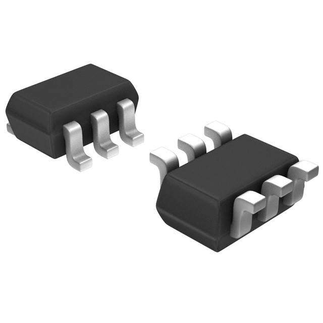
| 描述 | IC RES-PROG TEMP SWITCH SC70-6 |
| 产品分类 | 温度传感器,变送器 |
| 品牌 | Texas Instruments |
| 数据手册 | |
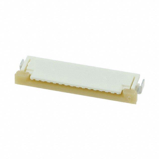
| 产品图片 |
|
| 产品型号 | TMP300BQDCKRQ1 |
| rohs | 无铅 / 符合限制有害物质指令(RoHS)规范要求 |
| 产品系列 | 自动,AEC-Q100 |
| 供应商器件封装 | SC-70-6 |
| 其它名称 | 296-36993-1 |
| 包装 | 剪切带 (CT) |
| 封装/外壳 | 6-TSSOP,SC-88,SOT-363 |
| 感应温度 | -40°C ~ 125°C |
| 标准包装 | 1 |
| 电压-电源 | 1.8 V ~ 18 V |
| 精度 | ±1°C |
| 输出类型 | 开路漏极 |


- 商务部:美国ITC正式对集成电路等产品启动337调查
- 曝三星4nm工艺存在良率问题 高通将骁龙8 Gen1或转产台积电
- 太阳诱电将投资9.5亿元在常州建新厂生产MLCC 预计2023年完工
- 英特尔发布欧洲新工厂建设计划 深化IDM 2.0 战略
- 台积电先进制程称霸业界 有大客户加持明年业绩稳了
- 达到5530亿美元!SIA预计今年全球半导体销售额将创下新高
- 英特尔拟将自动驾驶子公司Mobileye上市 估值或超500亿美元
- 三星加码芯片和SET,合并消费电子和移动部门,撤换高东真等 CEO
- 三星电子宣布重大人事变动 还合并消费电子和移动部门
- 海关总署:前11个月进口集成电路产品价值2.52万亿元 增长14.8%


PDF Datasheet 数据手册内容提取
TMP300B-Q1 www.ti.com SBOS586–DECEMBER2011 1.8V, Resistor-Programmable TEMPERATURE SWITCH and ANALOG OUT TEMPERATURE SENSOR in SC70 CheckforSamples:TMP300B-Q1 FEATURES DESCRIPTION 1 • ACCURACY:±1°C(typicalat+25°C) The TMP300B-Q1 is a low-power, 2 resistor-programmable, digital output temperature • PROGRAMMABLETRIPPOINT switch. It allows a threshold point to be set by adding • PROGRAMMABLEHYSTERESIS:5°C/10°C an external resistor. Two levels of hysteresis are • OPEN-DRAINOUTPUTS available. The TMP300B-Q1 has a VTEMP analog output that can be used as a testing point or in • LOW-POWER:110μA(max) temperature-compensationloops. • WIDEVOLTAGERANGE:+1.8Vto+18V With a supply voltage as low as 1.8V and low current • OPERATION:–40°Cto+150°C consumption, the TMP300B-Q1 is ideal for • ANALOGOUT:10mV/°C power-sensitivesystems. • SC70-6PACKAGE Available in two micropackages that have proven thermalcharacteristics,thispartgivesacompleteand APPLICATIONS simple solution for users who need simple and reliablethermalmanagement. • QUALIFIEDFORforAUTOMOTIVE APPLICATIONS • POWER-SUPPLYSYSTEMS • DC-DCMODULES • THERMALMONITORING • ELECTRONICPROTECTIONSYSTEMS V+ Proportional RPULL-UP 3mA toT TMP300B-Q1 A V T 1 6 V+ TEMP OUT SET T SET GND 2 5 V TEMP OUT 3 4 HYSTSET RSET 210kW(1) SC70-6 TMP300 HYST SET NOTE: (1)Thinfilm resistor with approximately 10% accuracy; however, this accuracy error is trimmed out at the factory. 1 Pleasebeawarethatanimportantnoticeconcerningavailability,standardwarranty,anduseincriticalapplicationsofTexas Instrumentssemiconductorproductsanddisclaimerstheretoappearsattheendofthisdatasheet. Alltrademarksarethepropertyoftheirrespectiveowners. 2 PRODUCTIONDATAinformationiscurrentasofpublicationdate. Copyright©2011,TexasInstrumentsIncorporated Products conform to specifications per the terms of the Texas Instruments standard warranty. Production processing does not necessarilyincludetestingofallparameters.
TMP300B-Q1 SBOS586–DECEMBER2011 www.ti.com This integrated circuit can be damaged by ESD. Texas Instruments recommends that all integrated circuits be handled with appropriateprecautions.Failuretoobserveproperhandlingandinstallationprocedurescancausedamage. ESDdamagecanrangefromsubtleperformancedegradationtocompletedevicefailure.Precisionintegratedcircuitsmaybemore susceptibletodamagebecauseverysmallparametricchangescouldcausethedevicenottomeetitspublishedspecifications. ORDERINGINFORMATION(1) ORDERABLEP/N T PACKAGE TOPSIDESYMBOL A TMP300BQDCKRQ1or -40°Cto125°C SC70-DCK|Reelof3000 SBG TMP300B-Q1 (1) ForthemostcurrentpackageandorderinginformationseethePackageOptionAddendumattheendofthisdocument,orseetheTI websiteatwww.ti.com. ABSOLUTE MAXIMUM RATINGS(1) VALUE UNIT SupplyVoltage V+ +18 V SignalInputTerminals,Voltage(2) –0.5to(V+)+0.5 V SignalInputTerminals,Current(2) ±10 mA OutputShort-Circuit(3) I Continuous SC Open-DrainOutput (V+)+0.5 V OperatingTemperature T –40to+150 °C A StorageTemperature T –55to+150 °C A JunctionTemperature T +150 °C J HumanBodyModel(HBM) 4000 V ESDRating ChargedDeviceModel(CDM) 1000 V MachineModel(MM) 200 V (1) Stressesabovetheseratingsmaycausepermanentdamage.Exposuretoabsolutemaximumconditionsforextendedperiodsmay degradedevicereliability.Thesearestressratingsonly,andfunctionaloperationofthedeviceattheseoranyotherconditionsbeyond thosespecifiedisnotsupported. (2) Inputterminalsarediode-clampedtothepower-supplyrails.Inputsignalsthatcanswingmorethan0.5Vbeyondthesupplyrailsshould becurrentlimitedto10mAorless. (3) Short-circuittoground. 2 SubmitDocumentationFeedback Copyright©2011,TexasInstrumentsIncorporated ProductFolderLink(s):TMP300B-Q1
TMP300B-Q1 www.ti.com SBOS586–DECEMBER2011 ELECTRICAL CHARACTERISTICS AtV =3.3VandT =–40°Cto+125°C,unlessotherwisenoted. S A TMP300B-Q1 PARAMETER TESTCONDITIONS MIN TYP MAX UNIT TEMPERATUREMEASUREMENT VS=2.35Vto18V –40 +125 °C MeasurementRange 100× VS=1.8Vto2.35V –40 (VS–0.95) °C TRIPPOINT TotalAccuracy TA=–40°Cto+125°C ±2 ±6 °C RSETEquation TCisin°C RSET=10(50+TC)/3 kΩ HYSTERESISSETINPUT LOWThreshold(1) 0.4 V HIGHThreshold(1) VS–0.4 V HYSTSET=GND 5 °C ThresholdHysteresis HYSTSET=VS 10 °C DIGITALOUTPUT LogicFamily CMOS Open-DrainLeakageCurrent(1) OUT=VS 10 μA LogicLevels VOL VS=1.8Vto18V,ISINK=5mA 0.3 V ANALOGOUTPUT Accuracy ±2 ±5 °C TemperatureSensitivity 10 mV/°C OutputVoltage(1) TA=+25°C 720 750 780 mV VTEMPPinOutputResistance 210 kΩ POWERSUPPLY QuiescentCurrent(2) IQ TAV=S–=410.°8CVtoto+1182V5,°C 110 μA TEMPERATURERANGE VS=2.35Vto18V –40 +125 °C SpecifiedRange TA 100× VS=1.8Vto2.35V –40 (VS–0.95) °C VS=2.35Vto18V –40 +150 °C OperatingRange TA 100× VS=1.8Vto2.35V –50 (VS–0.95) °C ThermalResistance θJA SC70 250 °C/W SOT23-6 180 °C/W (1) Specifiedbydesign.Notproductiontested. (2) SeeFigure1fortypicalquiescentcurrent. Copyright©2011,TexasInstrumentsIncorporated SubmitDocumentationFeedback 3 ProductFolderLink(s):TMP300B-Q1
TMP300B-Q1 SBOS586–DECEMBER2011 www.ti.com TYPICAL CHARACTERISTICS AtV =5V,unlessotherwisenoted. S QUIESCENTCURRENTOVERTEMPERATUREAND SUPPLY R SHIFTDUETOR TOLERANCE SET SET 95 2.0 T + 1% ERROR 1.5 85 V = 18V 1.0 S 0.5 I(A)mQ 7655 VS= 3.3V °Error (C) -0.05 TTEERRRROORR+- 00..11%% VS= 1.8V -1.0 55 -1.5 T -1% ERROR 45 -2.0 -40 -25 0 25 50 75 100 125 -40 -25 0 25 50 75 100 125 Temperature (°C) Temperature (°C) Figure1. Figure2. R vsTEMPERATURE TYPICALTRIPERROR SET 700 4.0 600 3.0 2.0 500 1.0 W) 400 C) R(kSET 300 °Error ( -1.00 200 -2.0 100 -3.0 0 -4.0 -40 -25 0 25 50 75 100 125 -40 -25 0 25 50 75 100 125 Temperature (°C) Temperature (°C) Figure3. Figure4. TYPICALANALOGOUTPUTERROR ANALOGPSROVERTEMPERATURE 3.0 0.10 2.5 0.08 2.0 0.06 1.5 T is +85°C for V = 1.8V to 3.3V MAX S 0.04 1.0 °Error (C) --001...5050 °Error(C/V) --000...0002420 3.3V to 18V -1.5 -2.0 -0.06 -2.5 -0.08 -3.0 -0.10 -40 -25 0 25 50 75 100 125 -40 -25 0 25 50 75 100 125 Temperature (°C) Temperature (°C) Figure5. Figure6. 4 SubmitDocumentationFeedback Copyright©2011,TexasInstrumentsIncorporated ProductFolderLink(s):TMP300B-Q1
TMP300B-Q1 www.ti.com SBOS586–DECEMBER2011 TYPICAL CHARACTERISTICS (continued) AtV =5V,unlessotherwisenoted. S TRIPPSROVERTEMPERATURE 0.10 0.08 0.06 0.04 V) 0.02 C/ 3.3V to 18V °( 0 or Err -0.02 -0.04 T is +85°C for V = 1.8V to 3.3V -0.06 MAX S -0.08 -0.10 -40 -25 0 25 50 75 100 125 Temperature (°C) Figure7. Copyright©2011,TexasInstrumentsIncorporated SubmitDocumentationFeedback 5 ProductFolderLink(s):TMP300B-Q1
TMP300B-Q1 SBOS586–DECEMBER2011 www.ti.com APPLICATIONS INFORMATION To set the TMP300B-Q1 to trip at a preset value, The TMP300B-Q1 is a thermal sensor designed for calculate the R resistor value according to over-temperature protection circuits in electronic SET Equation1orEquation2: systems. The TMP300B-Q1 uses a set resistor to (T ´0.01 + 0.5) program the trip temperature of the digital output. An SET R = additional high-impedance (210kΩ) analog voltage SET 3e-6 (1) outputprovidesthetemperaturereading. WhereT isin°C;or SET CALCULATING R 10(50 + T ) SET R in kW= SET The set resistor (R ) provides a threshold voltage SET 3 (2) SET for the comparator input. The TMP300B-Q1 trips WhereT isin°C. when the V pin exceeds the T voltage. The SET TEMP SET value of the set resistor is determined by the analog USING V TO TRIP THE DIGITAL OUTPUT outputfunctionandthe3μAinternalbiascurrent. TEMP The analog voltage output can also serve as a voltage input that forces a trip of the digital output to simulate a thermal event. This simulation facilitates easy system design and test of thermal safety circuits,asshowninFigure8. V+ Proportional 3mA to T A Voltage source VTEMP OUT to test trip point. Open-Drain Control T SET R INT R 210kW SET TMP300 HYST SET Figure8. ApplyingVoltagetoTripDigitalOutput 6 SubmitDocumentationFeedback Copyright©2011,TexasInstrumentsIncorporated ProductFolderLink(s):TMP300B-Q1
TMP300B-Q1 www.ti.com SBOS586–DECEMBER2011 ANALOG TEMPERATURE OUTPUT USING A DAC TO SET THE TRIP POINT The analog out or V pin is high-impedance The trip point is easily converted by changing the TEMP (210kΩ). Avoid loading this pin to prevent degrading digital-to-analog converter (DAC) code. This the analog out value or trip point. Buffer the output of technique can be useful for control loops where a this pin when using it for direct thermal measurement. large thermal mass is being brought up to the set Figure9showsbufferingoftheanalogoutputsignal. temperature and the OUT pin is used to control the heating element. The analog output can be monitored in a control algorithm that adjusts the set temperature to prevent overshoot. Trip set voltage error versus temperature is shown in Figure 10, which shows error OPA335 Analog Out in °C of the comparator input over temperature. An V+ alternative method of setting the trip point by using a DACisshowninFigure11. 1.00 Proportional 3mA to TA 0.75 V C) TEMP OUT °or ( 0.50 TSET Err 0.25 e ag 0 210kW olt et V -0.25 S TMP300 Trip -0.50 HYST -0.75 SET -1.00 -50 -25 0 25 50 75 100 125 Figure9. BufferingtheAnalogOutputSignal Temperature (°C) Figure10. TripSetVoltageErrorvsTemperature V+ Proportional 3mA to T A Voltage source VTEMP OUT to test trip point. Open-Drain Control T SET 210kW DAC8560 TMP300 HYST SET Figure11. DACGeneratestheVoltage-DrivingT Pin SET Copyright©2011,TexasInstrumentsIncorporated SubmitDocumentationFeedback 7 ProductFolderLink(s):TMP300B-Q1
TMP300B-Q1 SBOS586–DECEMBER2011 www.ti.com HYSTERESIS Bypass capacitors should be used on the supplies as The hysteresis pin has two settings. Grounding wellasontheR andanalogout(V )pinswhen SET TEMP HYST results in 5°C of hysteresis. Connecting it to in noisy environments, as shown in Figure 14. These SET V results in 10°C of hysteresis. Hysteresis error capacitors reduce premature triggering of the S variation over temperature is shown in Figure 12 and comparator. Figure13. 5 5 4 4 3 3 2 Maximum 2 Maximum C) 1 °or (C) 10 °Error ( -01 Err -1 -2 Average Minimum Average Minimum -2 -3 -3 -4 -4 -5 -5 -50 -25 0 25 50 75 100 125 -50 -25 0 25 50 75 100 125 Temperature (°C) Temperature (°C) Figure13. 10°CHysteresisErrorvsTemperature Figure12. 5°CHysteresisErrorvsTemperature V+ Proportional 3mA to T A V TEMP OUT Open-Drain Control T SET C BYPASS 210kW C R BYPASS SET TMP300 HYST SET Figure14. BypassCapacitorsPreventEarlyComparatorTogglingDuetoCircuitBoardNoise 8 SubmitDocumentationFeedback Copyright©2011,TexasInstrumentsIncorporated ProductFolderLink(s):TMP300B-Q1
PACKAGE OPTION ADDENDUM www.ti.com 6-Feb-2020 PACKAGING INFORMATION Orderable Device Status Package Type Package Pins Package Eco Plan Lead/Ball Finish MSL Peak Temp Op Temp (°C) Device Marking Samples (1) Drawing Qty (2) (6) (3) (4/5) TMP300BQDCKRQ1 ACTIVE SC70 DCK 6 3000 Green (RoHS NIPDAU Level-1-260C-UNLIM -40 to 125 SBG & no Sb/Br) (1) The marketing status values are defined as follows: ACTIVE: Product device recommended for new designs. LIFEBUY: TI has announced that the device will be discontinued, and a lifetime-buy period is in effect. NRND: Not recommended for new designs. Device is in production to support existing customers, but TI does not recommend using this part in a new design. PREVIEW: Device has been announced but is not in production. Samples may or may not be available. OBSOLETE: TI has discontinued the production of the device. (2) RoHS: TI defines "RoHS" to mean semiconductor products that are compliant with the current EU RoHS requirements for all 10 RoHS substances, including the requirement that RoHS substance do not exceed 0.1% by weight in homogeneous materials. Where designed to be soldered at high temperatures, "RoHS" products are suitable for use in specified lead-free processes. TI may reference these types of products as "Pb-Free". RoHS Exempt: TI defines "RoHS Exempt" to mean products that contain lead but are compliant with EU RoHS pursuant to a specific EU RoHS exemption. Green: TI defines "Green" to mean the content of Chlorine (Cl) and Bromine (Br) based flame retardants meet JS709B low halogen requirements of <=1000ppm threshold. Antimony trioxide based flame retardants must also meet the <=1000ppm threshold requirement. (3) MSL, Peak Temp. - The Moisture Sensitivity Level rating according to the JEDEC industry standard classifications, and peak solder temperature. (4) There may be additional marking, which relates to the logo, the lot trace code information, or the environmental category on the device. (5) Multiple Device Markings will be inside parentheses. Only one Device Marking contained in parentheses and separated by a "~" will appear on a device. If a line is indented then it is a continuation of the previous line and the two combined represent the entire Device Marking for that device. (6) Lead/Ball Finish - Orderable Devices may have multiple material finish options. Finish options are separated by a vertical ruled line. Lead/Ball Finish values may wrap to two lines if the finish value exceeds the maximum column width. Important Information and Disclaimer:The information provided on this page represents TI's knowledge and belief as of the date that it is provided. TI bases its knowledge and belief on information provided by third parties, and makes no representation or warranty as to the accuracy of such information. Efforts are underway to better integrate information from third parties. TI has taken and continues to take reasonable steps to provide representative and accurate information but may not have conducted destructive testing or chemical analysis on incoming materials and chemicals. TI and TI suppliers consider certain information to be proprietary, and thus CAS numbers and other limited information may not be available for release. In no event shall TI's liability arising out of such information exceed the total purchase price of the TI part(s) at issue in this document sold by TI to Customer on an annual basis. OTHER QUALIFIED VERSIONS OF TMP300-Q1 : Addendum-Page 1
PACKAGE OPTION ADDENDUM www.ti.com 6-Feb-2020 •Catalog: TMP300 NOTE: Qualified Version Definitions: •Catalog - TI's standard catalog product Addendum-Page 2
PACKAGE MATERIALS INFORMATION www.ti.com 3-Aug-2017 TAPE AND REEL INFORMATION *Alldimensionsarenominal Device Package Package Pins SPQ Reel Reel A0 B0 K0 P1 W Pin1 Type Drawing Diameter Width (mm) (mm) (mm) (mm) (mm) Quadrant (mm) W1(mm) TMP300BQDCKRQ1 SC70 DCK 6 3000 179.0 8.4 2.2 2.5 1.2 4.0 8.0 Q3 PackMaterials-Page1
PACKAGE MATERIALS INFORMATION www.ti.com 3-Aug-2017 *Alldimensionsarenominal Device PackageType PackageDrawing Pins SPQ Length(mm) Width(mm) Height(mm) TMP300BQDCKRQ1 SC70 DCK 6 3000 203.0 203.0 35.0 PackMaterials-Page2
None
None
IMPORTANTNOTICEANDDISCLAIMER TI PROVIDES TECHNICAL AND RELIABILITY DATA (INCLUDING DATASHEETS), DESIGN RESOURCES (INCLUDING REFERENCE DESIGNS), APPLICATION OR OTHER DESIGN ADVICE, WEB TOOLS, SAFETY INFORMATION, AND OTHER RESOURCES “AS IS” AND WITH ALL FAULTS, AND DISCLAIMS ALL WARRANTIES, EXPRESS AND IMPLIED, INCLUDING WITHOUT LIMITATION ANY IMPLIED WARRANTIES OF MERCHANTABILITY, FITNESS FOR A PARTICULAR PURPOSE OR NON-INFRINGEMENT OF THIRD PARTY INTELLECTUAL PROPERTY RIGHTS. These resources are intended for skilled developers designing with TI products. You are solely responsible for (1) selecting the appropriate TI products for your application, (2) designing, validating and testing your application, and (3) ensuring your application meets applicable standards, and any other safety, security, or other requirements. These resources are subject to change without notice. TI grants you permission to use these resources only for development of an application that uses the TI products described in the resource. Other reproduction and display of these resources is prohibited. No license is granted to any other TI intellectual property right or to any third party intellectual property right. TI disclaims responsibility for, and you will fully indemnify TI and its representatives against, any claims, damages, costs, losses, and liabilities arising out of your use of these resources. TI’s products are provided subject to TI’s Terms of Sale (www.ti.com/legal/termsofsale.html) or other applicable terms available either on ti.com or provided in conjunction with such TI products. TI’s provision of these resources does not expand or otherwise alter TI’s applicable warranties or warranty disclaimers for TI products. Mailing Address: Texas Instruments, Post Office Box 655303, Dallas, Texas 75265 Copyright © 2020, Texas Instruments Incorporated