ICGOO在线商城 > 集成电路(IC) > 线性 - 音頻放大器 > TDA7052AT/N2,118

 Datasheet下载
- 型号: TDA7052AT/N2,118
- 制造商: NXP Semiconductors
- 库位|库存: xxxx|xxxx
- 要求:
| 数量阶梯 | 香港交货 | 国内含税 |
| +xxxx | $xxxx | ¥xxxx |
查看当月历史价格
查看今年历史价格
TDA7052AT/N2,118产品简介:
ICGOO电子元器件商城为您提供TDA7052AT/N2,118由NXP Semiconductors设计生产,在icgoo商城现货销售,并且可以通过原厂、代理商等渠道进行代购。 TDA7052AT/N2,118价格参考。NXP SemiconductorsTDA7052AT/N2,118封装/规格:线性 - 音頻放大器, Amplifier IC 1-Channel (Mono) Class AB 8-SO。您可以下载TDA7052AT/N2,118参考资料、Datasheet数据手册功能说明书,资料中有TDA7052AT/N2,118 详细功能的应用电路图电压和使用方法及教程。
NXP USA Inc. 的 TDA7052AT/N2,118 是一款低电压单声道D类音频功率放大器,属于线性-音频放大器类别。该器件主要设计用于便携式音频设备,适用于对尺寸和功耗敏感的应用场景。

典型应用场景包括:便携式收音机、小型蓝牙音箱、儿童电子玩具、电话听筒放大器、助听设备以及家用电器中的语音提示系统(如微波炉、洗衣机等人机交互提示音输出)。由于其采用D类放大架构,具有较高的效率,可减少电池消耗,非常适合使用电池供电的设备。

TDA7052AT/N2,118 支持2.7V至16V宽电压范围工作,输出功率可达1瓦(在8Ω负载下),具备低失真和良好信噪比特性,确保清晰的音频输出。此外,该芯片集成度高,外围元件少,有助于简化电路设计并节省PCB空间。

其封装形式为DIP7(双列直插式),便于手工焊接与维修,适合中小批量生产应用。同时,芯片内置过热和短路保护功能,提升了系统可靠性。

综上,TDA7052AT/N2,118 特别适用于低成本、低功耗、小体积的消费类音频产品,是中低端便携音频设备中的理想选择。
| 参数 | 数值 |
| 产品目录 | 集成电路 (IC)半导体 |
| 描述 | IC AMP AUDIO 1.1W MONO AB 8SOIC音频放大器 0.5W BTL MONO AMP W/VOL CTRL |
| 产品分类 | |
| 品牌 | NXP Semiconductors |
| 产品手册 | http://www.nxp.com/documents/data_sheet/TDA7052A_AT.pdf?ecmp=mouser |
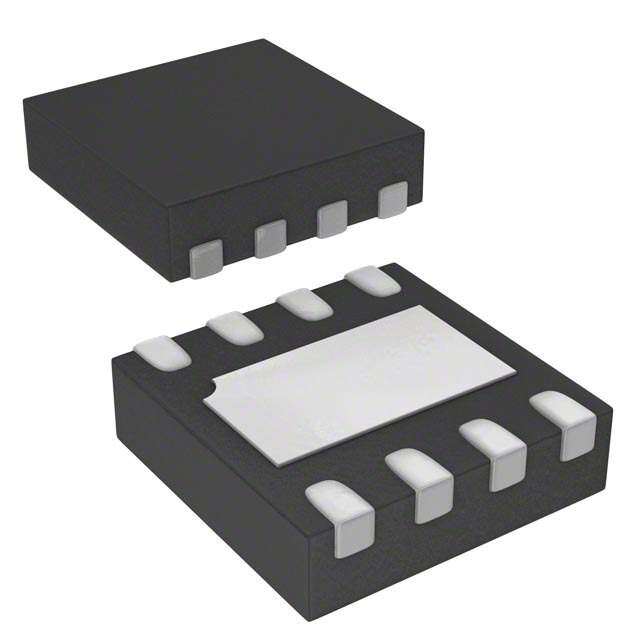
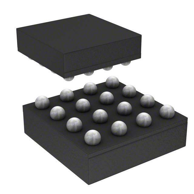
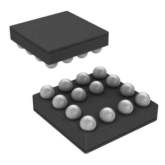
| 产品图片 |
|
| rohs | 符合RoHS无铅 / 符合限制有害物质指令(RoHS)规范要求 |
| 产品系列 | 音频 IC,音频放大器,NXP Semiconductors TDA7052AT/N2,118- |
| 数据手册 | |
| 产品型号 | TDA7052AT/N2,118 |
| PCN封装 | |
| PCN组件/产地 | |
| Pd-功率耗散 | 800 mW |
| THD+噪声 | 0.3 % |
| 不同负载时的最大输出功率x通道数 | 550mW x 1 @ 16 欧姆 |
| 产品 | Audio Amplifiers |
| 产品目录页面 | |
| 产品种类 | 音频放大器 |
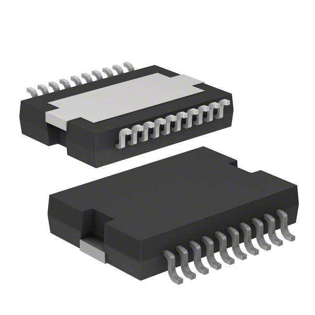
| 供应商器件封装 | 8-SO |
| 其它名称 | 568-1139-1 |
| 包装 | 剪切带 (CT) |
| 商标 | NXP Semiconductors |
| 增益 | 35.5 dB |
| 安装类型 | 表面贴装 |
| 安装风格 | SMD/SMT |
| 封装 | Reel |
| 封装/外壳 | 8-SOIC(0.154",3.90mm 宽) |
| 封装/箱体 | SO-8 |
| 工作温度 | -40°C ~ 85°C (TA) |
| 工作电源电压 | 5 V, 9 V, 12 V |
| 工厂包装数量 | 2500 |
| 最大功率耗散 | 800 mW |
| 最大工作温度 | + 85 C |
| 最小工作温度 | - 40 C |
| 标准包装 | 1 |
| 特性 | 消除爆音,静音,短路保护和热保护,音量控制 |
| 电压-电源 | 4.5 V ~ 18 V |
| 电源电压-最大 | 18 V |
| 电源电压-最小 | 4.5 V |
| 电源电流 | 7 mA |
| 电源类型 | Single |
| 类 | Class-AB |
| 类型 | AB 类 |
| 输入信号类型 | Single |
| 输出信号类型 | Differential |
| 输出功率 | 550 mW |
| 输出类型 | 1-通道(单声道) |
| 零件号别名 | TDA7052ATD-T |
| 音频负载电阻 | 16 Ohms |


PDF Datasheet 数据手册内容提取
INTEGRATED CIRCUITS DATA SHEET TDA7052A/AT 1 W BTL mono audio amplifier with DC volume control Product specification July 1994 File under Integrated circuits, IC01
Philips Semiconductors Product specification 1 W BTL mono audio amplifier with DC TDA7052A/AT volume control FEATURES GENERAL DESCRIPTION • DC volume control The TDA7052A/AT are mono BTL output amplifiers with • Few external components DC volume control. They are designed for use in TV and monitors, but also suitable for battery-fed portable • Mute mode recorders and radios. • Thermal protection • Short-circuit proof Missing Current Limiter (MCL) • No switch-on and off clicks A MCL protection circuit is built-in. The MCL circuit is • Good overall stability activated when the difference in current between the output terminal of each amplifier exceeds 100 mA (typical • Low power consumption 300 mA). This level of 100 mA allows for headphone • Low HF radiation applications (single-ended). • ESD protected on all pins QUICK REFERENCE DATA SYMBOL PARAMETERS CONDITIONS MIN. TYP. MAX. UNIT V positive supply voltage range 4.5 - 18 V P P output power O TDA7052A R = 8W ; V = 6V 1.0 1.1 - W L P TDA7052AT R = 16W ; V = 6V 0.5 0.55 - W L P G maximum total voltage gain 34.5 35.5 36.5 dB v f gain control range 75 80 - dB I total quiescent current V = 6V; R =¥ - 7 12 mA P P L THD total harmonic distortion TDA7052A P = 0.5W - 0.3 1 % O TDA7052AT P = 0.25W - 0.3 1 % O ORDERING INFORMATION PACKAGE EXTENDED TYPE NUMBER PINS PIN POSITION MATERIAL CODE TDA7052A 8 DIL plastic SOT97(1) TDA7052AT 8 mini-pack plastic SOT96A(2) Notes 1. SOT97-1; 1996September10. 2. SOT96-1; 1996September10. July 1994 2
Philips Semiconductors Product specification 1 W BTL mono audio amplifier with DC TDA7052A/AT volume control VP handbook, full pagewidth 1 7 n.c. TDA7052A TDA7052AT I + i 5 positive output 2 positive input DC volume 4 control I – i 8 negative output STABILIZER TEMPERATURE V PROTECTION ref 3 6 MCD385 - 1 signal power ground ground Fig.1 Block diagram. PINNING SYMBOL PIN DESCRIPTION handbook, halfpage VP 1 positive supply voltage VP 1 8 OUT – IN+ 2 positive input IN + 2 7 n.c. TDA7052A GND1 3 signal ground TDA7052AT GND1 3 6 GND2 VC 4 DC volume control VC 4 5 OUT + OUT+ 5 positive output GND2 6 power ground MCD384 n.c 7 not connected Fig.2 Pin configuration. OUT- 8 negative output July 1994 3
Philips Semiconductors Product specification 1 W BTL mono audio amplifier with DC TDA7052A/AT volume control FUNCTIONAL DESCRIPTION Thus a reduced power supply with smaller capacitors can be used which results in cost savings. The TDA7052A/AT are mono BTL output amplifiers with DC volume control, designed for use in TV and monitors For portable applications there is a trend to decrease the but also suitable for battery fed portable recorders and supply voltage, resulting in a reduction of output power at radios. conventional output stages. Using the BTL principle increases the output power. In conventional DC volume circuits the control or input stage is AC coupled to the output stage via external The maximum gain of the amplifier is fixed at 35.5dB. The capacitors to keep the offset voltage low. DC volume control stage has a logarithmic control characteristic. In the TDA7052A/AT the DC volume control stage is integrated into the input stage so that no coupling The total gain can be controlled from 35.5dB to- 44dB. If capacitors are required and yet a low offset voltage is the DC volume control voltage is below 0.3V, the device maintained. At the same time the minimum supply remains switches to the mute mode. low. The amplifier is short-circuit proof to ground, V and P The BTL principle offers the following advantages: across the load. Also a thermal protection circuit is • Lower peak value of the supply current implemented. If the crystal temperature rises above +150(cid:176) C the gain will be reduced, so the output power is • The frequency of the ripple on the supply voltage is twice reduced. the signal frequency. Special attention is given to switch on and off clicks, low HF radiation and a good overall stability. LIMITING VALUES In accordance with the Absolute Maximum System (IEC 134) SYMBOL PARAMETER CONDITIONS MIN. MAX. UNIT V supply voltage range - 18 V P I repetitive peak output current - 1.25 A ORM I non-repetitive peak output current - 1.5 A OSM P total power dissipation T £ 25% tot amb TDA7052A - 1.25 W TDA7052AT - 0.8 W T operating ambient temperature range - 40 +85 (cid:176) C amb T storage temperature range - 55 +150 (cid:176) C stg T virtual junction temperature - +150 (cid:176) C vj T short-circuit time - 1 hr sc V input voltage pin 2 - 8 V 2 V input voltage pin 4 - 8 V 4 July 1994 4
Philips Semiconductors Product specification 1 W BTL mono audio amplifier with DC TDA7052A/AT volume control THERMAL RESISTANCE SYMBOL PARAMETER THERMAL RESISTANCE R from junction to ambient in free air th j-a TDA7052A 100 K/W TDA7052AT 155 K/W Notes to the thermal resistance TDA7052A: V = 6V; R = 8W . The maximum sine-wave dissipation is 0.9W. P L Therefore T = 150- 100· 0.9 = 60(cid:176) C. amb(max) TDA7052AT: V = 6V; R = 16W . The maximum sine-wave dissipation is 0.46W. P L Therefore T = 150- 155· 0.46 = 78(cid:176) C. amb(max) July 1994 5
Philips Semiconductors Product specification 1 W BTL mono audio amplifier with DC TDA7052A/AT volume control CHARACTERISTICS V = 6V; T = 25(cid:176) C; f = 1kHz; TDA7052A: R = 8W ; TDA7052AT: R = 16W ; unless otherwise specified (see Fig.6). P amb L L SYMBOL PARAMETER CONDITIONS MIN. TYP. MAX. UNIT V positive supply voltage range 4.5 - 18 V P I total quiescent current V = 6V; R =¥ - 7 12 mA P P L note 1 Maximum gain; V = 1.4V 4 P output power THD = 10% O TDA7052A 1.0 1.1 - W TDA7052AT 0.5 0.55 - W THD total harmonic distortion TDA7052A P = 0.5W - 0.3 1 % O TDA7052AT P = 0.25W - 0.3 1 % O G voltage gain 34.5 35.5 36.5 dB v V input signal handling V = 0.8V; THD< 1% 0.5 0.65 - V I 4 V noise output voltage (RMS value) f = 500kHz; note 2 - 210 - m V no(rms) B bandwidth - 1 dB - 20Hz to - 300kHz SVRR supply voltage ripple rejection note 3 38 46 - dB |V | DC output offset voltage - 0 150 mV off Z input impedance (pin 2) 15 20 25 kW I Minimum gain; V = 0.5V 4 G voltage gain - - 44 - dB v V noise output voltage (RMS value) note 4 - 20 30 m V no(rms) Mute position V output voltage in mute position V £ 0.3V; V = 600mV - - 30 m V O 4 I DC volume control f gain control range 75 80 - dB I control current V = 0.4V 60 70 80 m A 4 4 Notes to the characteristics 1. With a load connected to the outputs the quiescent current will increase, the maximum value of this increase being equal to the DC output offset voltage dividend by R . L 2. The noise output voltage (RMS value) at f = 500kHz is measured with R = 0W and bandwidth = 5kHz. S 3. The ripple rejection is measured with R = 0W and f = 100Hz to 10kHz. The ripple voltage of 200mV, (RMS value) S is applied to the positive supply rail. 4. The noise output voltage (RMS value) is measured with R = 5kW unweighted. S July 1994 6
Philips Semiconductors Product specification 1 W BTL mono audio amplifier with DC TDA7052A/AT volume control MCD388 MCD389 - 1 40 1000 handbgooakin, halfpage hVanndobiosoek, halfpage (dB) (µV) 20 800 0 600 – 20 400 – 40 200 – 60 – 80 0 0 0.4 0.8 1.2 1.6 2.0 0 0.4 0.8 1.2 1.6 2.0 V (V) V (V) 4 4 Fig.4 Noise output voltage as a function of DC Fig.3 Gain control as a function of DC volume control. volume control. MCD390 - 1 100 handbook, halfpage I4 (µA) 60 20 – 20 – 60 – 100 0 0.4 0.8 1.2 1.6 2.0 V4 (V) Fig.5 Control current as a function of DC volume control. July 1994 7
Philips Semiconductors Product specification 1 W BTL mono audio amplifier with DC TDA7052A/AT volume control APPLICATION INFORMATION (1) handbook, full pagewidth VP = 6 V 100 nF 220 µF 1 7 n.c. TDA7052A TDA7052AT I + i 5 positive input 0.47 µF 2 R L = 8 Ω 4 (TDA7052A) R L = 16 Ω (TDA7052A/AT) I – i 8 R 5 kΩ S STABILIZER TEMPERATURE V PROTECTION ref DC volume 3 6 control MCD386 - 1 This capacitor can be omitted if the 220m F electrolytic capacitor is connected close to pin 1. ground Fig.6 Test and application diagram. handbook, halfpage volume control 4 1 m F 1 MW MCD387 Fig.7 Application with potentiometer as volume control; maximum gain = 30dB. July 1994 8
Philips Semiconductors Product specification 1 W BTL mono audio amplifier with DC TDA7052A/AT volume control PACKAGE OUTLINES DIP8: plastic dual in-line package; 8 leads (300 mil) SOT97-1 D ME e n a pl g n eati A2 A s L A1 c Z w M b1 e (e ) 1 MH b b2 8 5 pin 1 index E 1 4 0 5 10 mm scale DIMENSIONS (inch dimensions are derived from the original mm dimensions) UNIT mAax. mAi n1 . mAa 2x . b b1 b2 c D(1) E(1) e e1 L ME MH w mZa(1x). 1.73 0.53 1.07 0.36 9.8 6.48 3.60 8.25 10.0 mm 4.2 0.51 3.2 2.54 7.62 0.254 1.15 1.14 0.38 0.89 0.23 9.2 6.20 3.05 7.80 8.3 inches 0.17 0.020 0.13 0.068 0.021 0.042 0.014 0.39 0.26 0.10 0.30 0.14 0.32 0.39 0.01 0.045 0.045 0.015 0.035 0.009 0.36 0.24 0.12 0.31 0.33 Note 1. Plastic or metal protrusions of 0.25 mm maximum per side are not included. OUTLINE REFERENCES EUROPEAN ISSUE DATE VERSION PROJECTION IEC JEDEC EIAJ 92-11-17 SOT97-1 050G01 MO-001AN 95-02-04 July 1994 9
Philips Semiconductors Product specification 1 W BTL mono audio amplifier with DC TDA7052A/AT volume control SO8: plastic small outline package; 8 leads; body width 3.9 mm SOT96-1 D E A X c y HE v M A Z 8 5 Q A2 A1 (A 3 ) A pin 1 index q Lp 1 4 L e w M detail X bp 0 2.5 5 mm scale DIMENSIONS (inch dimensions are derived from the original mm dimensions) UNIT mAax. A1 A2 A3 bp c D(1) E(2) e HE L Lp Q v w y Z(1) q 0.25 1.45 0.49 0.25 5.0 4.0 6.2 1.0 0.7 0.7 mm 1.75 0.25 1.27 1.05 0.25 0.25 0.1 0.10 1.25 0.36 0.19 4.8 3.8 5.8 0.4 0.6 0.3 8o 0.010 0.057 0.019 0.0100 0.20 0.16 0.244 0.039 0.028 0.028 0o inches 0.069 0.01 0.050 0.041 0.01 0.01 0.004 0.004 0.049 0.014 0.0075 0.19 0.15 0.228 0.016 0.024 0.012 Notes 1. Plastic or metal protrusions of 0.15 mm maximum per side are not included. 2. Plastic or metal protrusions of 0.25 mm maximum per side are not included. OUTLINE REFERENCES EUROPEAN ISSUE DATE VERSION PROJECTION IEC JEDEC EIAJ 95-02-04 SOT96-1 076E03S MS-012AA 97-05-22 July 1994 10
Philips Semiconductors Product specification 1 W BTL mono audio amplifier with DC TDA7052A/AT volume control SOLDERING Several techniques exist for reflowing; for example, thermal conduction by heated belt. Dwell times vary Introduction between 50and300seconds depending on heating There is no soldering method that is ideal for all IC method. Typical reflow temperatures range from packages. Wave soldering is often preferred when 215to250(cid:176) C. through-hole and surface mounted components are mixed Preheating is necessary to dry the paste and evaporate on one printed-circuit board. However, wave soldering is the binding agent. Preheating duration: 45minutes at not always suitable for surface mounted ICs, or for 45(cid:176) C. printed-circuits with high population densities. In these situations reflow soldering is often used. WAVESOLDERING This text gives a very brief insight to a complex technology. Wave soldering techniques can be used for all SO A more in-depth account of soldering ICs can be found in packages if the following conditions are observed: our“IC Package Databook” (order code 939865290011). • A double-wave (a turbulent wave with high upward pressure followed by a smooth laminar wave) soldering DIP technique should be used. SOLDERINGBYDIPPINGORBYWAVE • The longitudinal axis of the package footprint must be The maximum permissible temperature of the solder is parallel to the solder flow. 260(cid:176) C; solder at this temperature must not be in contact • The package footprint must incorporate solder thieves at with the joint for more than 5seconds. The total contact the downstream end. time of successive solder waves must not exceed 5seconds. During placement and before soldering, the package must be fixed with a droplet of adhesive. The adhesive can be The device may be mounted up to the seating plane, but applied by screen printing, pin transfer or syringe the temperature of the plastic body must not exceed the dispensing. The package can be soldered after the specified maximum storage temperature (Tstgmax). If the adhesive is cured. printed-circuit board has been pre-heated, forced cooling may be necessary immediately after soldering to keep the Maximum permissible solder temperature is 260(cid:176) C, and temperature within the permissible limit. maximum duration of package immersion in solder is 10seconds, if cooled to less than 150(cid:176) C within 6seconds. Typical dwell time is 4seconds at 250(cid:176) C. REPAIRINGSOLDEREDJOINTS A mildly-activated flux will eliminate the need for removal Apply a low voltage soldering iron (less than24V) to the of corrosive residues in most applications. lead(s) of the package, below the seating plane or not more than 2mm above it. If the temperature of the soldering iron bit is less than 300(cid:176) C it may remain in REPAIRINGSOLDEREDJOINTS contact for up to 10seconds. If the bit temperature is Fix the component by first soldering two diagonally- between 300and400(cid:176) C, contact may be up to 5seconds. opposite end leads. Use only a low voltage soldering iron (less than24V) applied to the flat part of the lead. Contact SO time must be limited to 10seconds at up to 300(cid:176) C. When using a dedicated tool, all other leads can be soldered in REFLOWSOLDERING one operation within 2 to 5seconds between Reflow soldering techniques are suitable for all SO 270and320(cid:176) C. packages. Reflow soldering requires solder paste (a suspension of fine solder particles, flux and binding agent) to be applied to the printed-circuit board by screen printing, stencilling or pressure-syringe dispensing before package placement. July 1994 11
Philips Semiconductors Product specification 1 W BTL mono audio amplifier with DC TDA7052A/AT volume control DEFINITIONS Data sheet status Objective specification This data sheet contains target or goal specifications for product development. Preliminary specification This data sheet contains preliminary data; supplementary data may be published later. Product specification This data sheet contains final product specifications. Limiting values Limiting values given are in accordance with the Absolute Maximum Rating System (IEC 134). Stress above one or more of the limiting values may cause permanent damage to the device. These are stress ratings only and operation of the device at these or at any other conditions above those given in the Characteristics sections of the specification is not implied. Exposure to limiting values for extended periods may affect device reliability. Application information Where application information is given, it is advisory and does not form part of the specification. LIFE SUPPORT APPLICATIONS These products are not designed for use in life support appliances, devices, or systems where malfunction of these products can reasonably be expected to result in personal injury. Philips customers using or selling these products for use in such applications do so at their own risk and agree to fully indemnify Philips for any damages resulting from such improper use or sale. July 1994 12