ICGOO在线商城 > 集成电路(IC) > 线性 - 音頻放大器 > TPA3110D2PWP
 Datasheet下载
- 型号: TPA3110D2PWP
- 制造商: Texas Instruments
- 库位|库存: xxxx|xxxx
- 要求:
| 数量阶梯 | 香港交货 | 国内含税 |
| +xxxx | $xxxx | ¥xxxx |
查看当月历史价格
查看今年历史价格
TPA3110D2PWP产品简介:
ICGOO电子元器件商城为您提供TPA3110D2PWP由Texas Instruments设计生产,在icgoo商城现货销售,并且可以通过原厂、代理商等渠道进行代购。 TPA3110D2PWP价格参考。Texas InstrumentsTPA3110D2PWP封装/规格:线性 - 音頻放大器, Amplifier IC 2-Channel (Stereo) Class D 28-HTSSOP。您可以下载TPA3110D2PWP参考资料、Datasheet数据手册功能说明书,资料中有TPA3110D2PWP 详细功能的应用电路图电压和使用方法及教程。
Texas Instruments(德州仪器)的TPA3110D2PWP是一款高效的D类音频功率放大器,广泛应用于各种需要高音质、低功耗和小尺寸解决方案的场景。以下是其主要应用场景:

 1. 便携式音频设备
TPA3110D2PWP因其高效能和低功耗特性,特别适合用于便携式音频设备,如蓝牙音箱、便携式音响系统等。它能够在电池供电的情况下提供高质量的音频输出,同时延长电池寿命,确保用户在户外或移动环境中享受长时间的音乐体验。

 2. 智能家居设备
该放大器也适用于智能家居设备,例如智能音箱、智能电视等。它能够为这些设备提供清晰、强劲的音频输出,支持多种音频格式,并且可以通过数字输入接口与主控芯片无缝连接,简化设计并提高系统的集成度。

 3. 汽车音响系统
TPA3110D2PWP在汽车音响系统中也有广泛应用。它可以驱动多个扬声器,提供立体声或多声道音频输出,满足车内不同位置乘客的听觉需求。此外,它的高效能有助于减少热量产生,提升系统的稳定性和可靠性。

 4. 消费电子产品
包括平板电脑、笔记本电脑、游戏机等在内的消费电子产品也可以使用TPA3110D2PWP来增强音频表现。它不仅能够提供高保真的音频输出,还能通过内置的保护机制(如过热保护、短路保护等)确保设备的安全运行。

 5. 工业和专业音频设备
在一些专业音频设备中,如会议系统、公共广播系统等,TPA3110D2PWP同样表现出色。它能够提供稳定的音频放大,支持远距离传输,确保声音清晰、无失真,适用于会议室、礼堂、剧院等场所。

总之,TPA3110D2PWP凭借其高效能、低功耗、高音质等特点,适用于多种音频应用场景,能够满足不同领域对音频放大的需求。
| 参数 | 数值 |
| 产品目录 | 集成电路 (IC)半导体 |
| 描述 | IC AMP AUD PWR 15W STER 28HTSSOP音频放大器 15W Class D Stereo Amplifier |
| DevelopmentKit | TPA3110D2EVM |
| 产品分类 | |
| 品牌 | Texas Instruments |
| 产品手册 | http://www.ti.com/litv/slos528d |
| 产品图片 |
|
| rohs | 符合RoHS无铅 / 符合限制有害物质指令(RoHS)规范要求 |
| 产品系列 | 音频 IC,音频放大器,Texas Instruments TPA3110D2PWPSpeakerGuard™ |
| 数据手册 | |
| 产品型号 | TPA3110D2PWP |
| PCN组件/产地 | |
| THD+噪声 | 0.1 % |
| 不同负载时的最大输出功率x通道数 | 15W x 2 @ 8 欧姆 |
| 产品 | Class-D |
| 产品目录页面 | |
| 产品种类 | 音频放大器 |
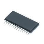
| 供应商器件封装 | 28-HTSSOP |
| 其它名称 | 296-24968-5 |
| 包装 | 管件 |
| 商标 | Texas Instruments |
| 增益 | 36 dB |
| 安装类型 | 表面贴装 |
| 安装风格 | SMD/SMT |
| 封装 | Tube |
| 封装/外壳 | 28-SOIC(0.173",4.40mm 宽)裸露焊盘 |
| 封装/箱体 | HTSSOP-28 |
| 工作温度 | -40°C ~ 85°C (TA) |
| 工作电源电压 | 9 V, 12 V, 15 V |
| 工厂包装数量 | 50 |
| 最大功率耗散 | 4480 mW |
| 最大工作温度 | + 85 C |
| 最小工作温度 | - 40 C |
| 标准包装 | 50 |
| 特性 | 差分输入,短路保护和热保护,关机 |
| 电压-电源 | 8 V ~ 26 V |
| 电源电压-最大 | 26 V |
| 电源电压-最小 | 8 V |
| 电源电流 | 32 mA |
| 电源类型 | Single |
| 类型 | D 类 |
| 系列 | TPA3110D2 |
| 输入信号类型 | Differential |
| 输出信号类型 | Differential |
| 输出功率 | 15 W |
| 输出类型 | 2 通道(立体声) |
| 音频负载电阻 | 8 Ohms |


- 商务部:美国ITC正式对集成电路等产品启动337调查
- 曝三星4nm工艺存在良率问题 高通将骁龙8 Gen1或转产台积电
- 太阳诱电将投资9.5亿元在常州建新厂生产MLCC 预计2023年完工
- 英特尔发布欧洲新工厂建设计划 深化IDM 2.0 战略
- 台积电先进制程称霸业界 有大客户加持明年业绩稳了
- 达到5530亿美元!SIA预计今年全球半导体销售额将创下新高
- 英特尔拟将自动驾驶子公司Mobileye上市 估值或超500亿美元
- 三星加码芯片和SET,合并消费电子和移动部门,撤换高东真等 CEO
- 三星电子宣布重大人事变动 还合并消费电子和移动部门
- 海关总署:前11个月进口集成电路产品价值2.52万亿元 增长14.8%


PDF Datasheet 数据手册内容提取
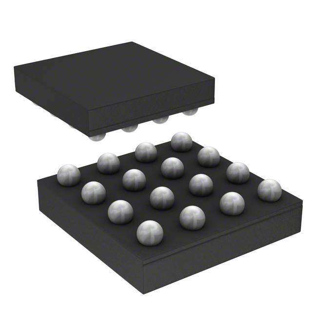
Product Order Technical Tools & Support & Folder Now Documents Software Community TPA3110D2 SLOS528F–JULY2009–REVISEDAPRIL2017 TPA3110D2 15-W Fil ter-Free Stereo Class-D Audio Power Amplifier With Speakerguard™ 1 Features 3 Description • 15-W/chintoan8-Ω Loadsat10%THD+NFrom The TPA3110D2 is a 15-W (per channel) efficient, 1 Class-D audio power amplifier for driving bridged-tied a16-VSupply stereo speakers. Advanced EMI Suppression • 10-W/chinto8-Ω Loadsat10%THD+NFroma Technology enables the use of inexpensive ferrite 13-VSupply bead filters at the outputs while meeting EMC • 30-Wintoa4-Ω MonoLoadat10%THD+NFrom requirements. SpeakerGuard™ speaker protection a16-VSupply circuitry includes an adjustable power limiter and a DC detection circuit. The adjustable power limiter • 90%EfficientClass-DOperationEliminatesNeed allows the user to set a "virtual" voltage rail lower forHeatSinks than the chip supply to limit the amount of current • WideSupplyVoltageRangeAllowsOperation through the speaker. The DC detect circuit measures From8Vto26V the frequency and amplitude of the PWM signal and • Filter-FreeOperation shuts off the output stage if the input capacitors are damagedorshortsexistontheinputs. • SpeakerGuard™SpeakerProtectionIncludes AdjustablePowerLimiterPlusDCProtection The TPA3110D2 can drive stereo speakers as low as 4 Ω. The high efficiency of the TPA3110D2, 90%, • FlowThroughPinOutFacilitatesEasyBoard eliminates the need for an external heat sink when Layout playingmusic. • RobustPin-to-PinShortCircuitProtectionand ThermalProtectionWithAutoRecoveryOption The outputs are also fully protected against shorts to GND, VCC, and output-to-output. The short-circuit • ExcellentTHD+N/Pop-FreePerformance protection and thermal protection includes an auto- • FourSelectable,FixedGainSettings recoveryfeature. • DifferentialInputs DeviceInformation(1) 2 Applications PARTNUMBER PACKAGE BODYSIZE(NOM) • Televisions TPA3110D2 HTSSOP(28) 9.70mm×4.40mm • ConsumerAudioEquipment (1) For all available packages, see the orderable addendum at theendofthedatasheet. TPA3110D2SimplifiedApplicationSchematic 1mF OUTL+ LINP TPA3110D2 Audio OUTL- LINN Source OUTR+ RINP OUTPL FFFEEERRRRRRIIITTTEEE 15W BBBEEEAAADDD OUTR- RINN OUTNL FFFIIILLLTTTEEERRR 8W GAIN0 GAIN1 OUTPR FFFEEERRRRRRIIITTTEEE 15W BBBEEEAAADDD OUTNR FFFIIILLLTTTEEERRR 8W PLIMIT PBTL FFaauulltt SSDD PVCC 8 to 26V 1 An IMPORTANT NOTICE at the end of this data sheet addresses availability, warranty, changes, use in safety-critical applications, intellectualpropertymattersandotherimportantdisclaimers.PRODUCTIONDATA.
TPA3110D2 SLOS528F–JULY2009–REVISEDAPRIL2017 www.ti.com Table of Contents 1 Features.................................................................. 1 9.2 FunctionalBlockDiagram.......................................14 2 Applications........................................................... 1 9.3 FeatureDescription.................................................15 3 Description............................................................. 1 9.4 DeviceFunctionalModes........................................20 4 RevisionHistory..................................................... 2 10 ApplicationandImplementation........................ 21 10.1 ApplicationInformation..........................................21 5 DeviceComparisonTable..................................... 4 10.2 TypicalApplications .............................................21 6 PinConfigurationandFunctions........................ 4 11 PowerSupplyRecommendations..................... 25 7 Specifications......................................................... 5 11.1 PowerSupplyDecoupling,C .............................25 7.1 AbsoluteMaximumRatings......................................5 S 12 Layout................................................................... 25 7.2 ESDRatings..............................................................6 12.1 LayoutGuidelines.................................................25 7.3 RecommendedOperatingConditions......................6 12.2 LayoutExample....................................................26 7.4 ThermalInformation..................................................6 13 DeviceandDocumentationSupport................. 27 7.5 DCCharacteristics:24V..........................................6 7.6 DCCharacteristics:12V..........................................7 13.1 DeviceSupport ....................................................27 7.7 ACCharacteristics:24V..........................................7 13.2 DocumentationSupport........................................27 7.8 ACCharacteristics:12V..........................................7 13.3 CommunityResources..........................................27 7.9 TypicalCharacteristics .............................................8 13.4 Trademarks...........................................................27 13.5 ElectrostaticDischargeCaution............................27 8 ParameterMeasurementInformation................14 13.6 Glossary................................................................27 9 DetailedDescription............................................ 14 14 Mechanical,Packaging,andOrderable 9.1 Overview.................................................................14 Information........................................................... 27 4 Revision History NOTE:Pagenumbersforpreviousrevisionsmaydifferfrompagenumbersinthecurrentversion. ChangesfromRevisionE(November2015)toRevisionF Page • AddedMeasurementnoteaddedtocharacterizationgraphs............................................................................................... 10 • AddedNewOutputPowervsSupplyVoltageCharacterizationgraph................................................................................ 10 • AddedfootnoteforheatsinkandEVM................................................................................................................................. 14 ChangesfromRevisionD(July2012)toRevisionE Page • AddedPinConfigurationandFunctionssection,ESDRatingstable,FeatureDescriptionsection,DeviceFunctional Modes,ApplicationandImplementationsection,PowerSupplyRecommendationssection,Layoutsection,Device andDocumentationSupportsection,andMechanical,Packaging,andOrderableInformationsection .............................. 1 ChangesfromRevisionC(August2010)toRevisionD Page • Added<10V/mstoV intheAbsoluteMaximumRatingstable,addedNote2.................................................................... 5 I • ChangedthePBTLSelectsection.Addedtext-"Thevoltageslew.......serieswiththeterminals.".................................... 19 • Addeda100kΩresistortoAVCCPin14andNote1toFigure46...................................................................................... 24 ChangesfromRevisionB(July2010)toRevisionC Page • ReplacedtheDissipationsRatingstablewiththeThermalInformationtable........................................................................ 6 ChangesfromRevisionA(July2009)toRevisionB Page • Addedslewrateadjustmentinformation.............................................................................................................................. 17 • AddedAVCCtoPin7ofFigure46...................................................................................................................................... 24 2 SubmitDocumentationFeedback Copyright©2009–2017,TexasInstrumentsIncorporated ProductFolderLinks:TPA3110D2
TPA3110D2 www.ti.com SLOS528F–JULY2009–REVISEDAPRIL2017 ChangesfromOriginal(July2009)toRevisionA Page • ChangedChangedtheStereoClass-DAmplifierwithBTLOutputandSingle-EndedInputillustrationFigure42- Correctedthepinnames...................................................................................................................................................... 21 • ChangedChangedtheStereoClass-DAmplifierwithPBTLOutputandSingle-EndedInputillustrationFigure46- Correctedthepinnames...................................................................................................................................................... 24 Copyright©2009–2017,TexasInstrumentsIncorporated SubmitDocumentationFeedback 3 ProductFolderLinks:TPA3110D2
TPA3110D2 SLOS528F–JULY2009–REVISEDAPRIL2017 www.ti.com 5 Device Comparison Table DEVICE SPEAKERAMP SPEAKERCHANNELS OUTPUTPOWER(W) ADDITIONALFEATURES NUMBER TYPE TPA3110D2 Stereo ClassD 15 Powerlimiter TPA3130D1 Stereo ClassD 15 TPA3118D2 Stereo ClassD 30 Powerlimiter TPA3116D1 Stereo ClassD 50 Powerlimiter 6 Pin Configuration and F unctions PWPPackage 28-PinHTSSOPWithPowerPAD™ TopView SD 1 28 PVCCL FAULT 2 27 PVCCL LINP 3 26 BSPL LINN 4 25 OUTPL GAIN0 5 24 PGND GAIN1 6 23 OUTNL AVCC 7 22 BSNL AGND 8 21 BSNR GVDD 9 20 OUTNR PLIMIT 10 19 PGND RINN 11 18 OUTPR RINP 12 17 BSPR NC 13 16 PVCCR PBTL 14 15 PVCCR Table1. PinFunctions PIN TYPE DESCRIPTION NO. NAME Shutdownlogicinputforaudioamp(LOW=outputsHi-Z,HIGH=outputsenabled).TTLlogiclevels 1 SD I withcompliancetoAVCC. Opendrainoutputusedtodisplayshortcircuitordcdetectfaultstatus.VoltagecomplianttoAVCC. 2 FAULT O Shortcircuitfaultscanbesettoauto-recoverybyconnectingFAULTpintoSDpin.Otherwise,both shortcircuitfaultsanddcdetectfaultsmustberesetbycyclingPVCC. 3 LINP I Positiveaudioinputforleftchannel.Biasedat3V. 4 LINN I Negativeaudioinputforleftchannel.Biasedat3V. 5 GAIN0 I Gainselectleastsignificantbit.TTLlogiclevelswithcompliancetoAVCC. 6 GAIN1 I Gainselectmostsignificantbit.TTLlogiclevelswithcompliancetoAVCC. 7 AVCC P Analogsupply 8 AGND — Analogsignalground.Connecttothethermalpad. High-sideFETgatedrivesupply.Nominalvoltageis7V.AlsoshouldbeusedassupplyforPLIMIT 9 GVDD O function. Powerlimitleveladjust.ConnectaresistordividerfromGVDDtoGNDtosetpowerlimit.Connect 10 PLIMIT I directlytoGVDDfornopowerlimit. 11 RINN I Negativeaudioinputforrightchannel.Biasedat3V. 12 RINP I Positiveaudioinputforrightchannel.Biasedat3V. 13 NC — Notconnected 14 PBTL I ParallelBTLmodeswitch 4 SubmitDocumentationFeedback Copyright©2009–2017,TexasInstrumentsIncorporated ProductFolderLinks:TPA3110D2
TPA3110D2 www.ti.com SLOS528F–JULY2009–REVISEDAPRIL2017 Table1. PinFunctions(continued) PIN TYPE DESCRIPTION NO. NAME PowersupplyforrightchannelH-bridge.Rightchannelandleftchannelpowersupplyinputsare 15 PVCCR P connectinternally. PowersupplyforrightchannelH-bridge.Rightchannelandleftchannelpowersupplyinputsare 16 PVCCR P connectinternally. 17 BSPR I BootstrapI/Oforrightchannel,positivehigh-sideFET. 18 OUTPR O Class-DH-bridgepositiveoutputforrightchannel. 19 PGND — PowergroundfortheH-bridges. 20 OUTNR O Class-DH-bridgenegativeoutputforrightchannel. 21 BSNR I BootstrapI/Oforrightchannel,negativehigh-sideFET. 22 BSNL I BootstrapI/Oforleftchannel,negativehigh-sideFET. 23 OUTNL O Class-DH-bridgenegativeoutputforleftchannel. 24 PGND — PowergroundfortheH-bridges. 25 OUTPL O Class-DH-bridgepositiveoutputforleftchannel. 26 BSPL I BootstrapI/Oforleftchannel,positivehigh-sideFET. PowersupplyforleftchannelH-bridge.Rightchannelandleftchannelpowersupplyinputsare 27 PVCCL P connectinternally. PowersupplyforleftchannelH-bridge.Rightchannelandleftchannelpowersupplyinputsare 28 PVCCL P connectinternally. 7 Specifications 7.1 Absolute Maximum Ratings overoperatingfree-airtemperaturerange(unlessotherwisenoted)(1) MIN MAX UNIT V Supplyvoltage AVCC,PVCC –0.3V 30V V CC V + –0.3V CC V 0.3V SD,GAIN0,GAIN1,PBTL,FAULT (2) <10 V Interfacepinvoltage V/ms I PLIMIT GVDD+ –0.3 V 0.3 RINN,RINP,LINN,LINP –0.3 6.3 V SeeThermal Continuoustotalpowerdissipation Information BTL:PVCC>15V 4.8 R MinimumLoadResistance BTL:PVCC≤15V 3.2 L PBTL 3.2 T Operatingfree-airtemperature –40 85 °C A T Operatingjunctiontemperaturerange(3) –40 150 °C J T Storagetemperature –65 150 °C stg (1) StressesbeyondthoselistedunderAbsoluteMaximumRatingsmaycausepermanentdamagetothedevice.Thesearestressratings only,whichdonotimplyfunctionaloperationofthedeviceattheseoranyotherconditionsbeyondthoseindicatedunderRecommended OperatingConditions.Exposuretoabsolute-maximum-ratedconditionsforextendedperiodsmayaffectdevicereliability. (2) Thevoltageslewrateofthesepinsmustberestrictedtonomorethan10V/ms.Forhigherslewrates,usea100-kΩresisterinseries withthepins. (3) TheTPA3110D2incorporatesanexposedthermalpadontheundersideofthechip.Thisactsasaheatsink,anditmustbeconnected toathermallydissipatingplaneforproperpowerdissipation.Failuretodosomayresultinthedevicegoingintothermalprotection shutdown.SeeTITechnicalBriefsSLMA002formoreinformationaboutusingtheTSSOPthermalpad. Copyright©2009–2017,TexasInstrumentsIncorporated SubmitDocumentationFeedback 5 ProductFolderLinks:TPA3110D2
TPA3110D2 SLOS528F–JULY2009–REVISEDAPRIL2017 www.ti.com 7.2 ESD Ratings VALUE UNIT Human-bodymodel(HBM),perANSI/ESDA/JEDECJS-001(1) ±2000 V(ESD) Electrostaticdischarge Charged-devicemodel(CDM),perJEDECspecificationJESD22- V C101(2) ±500 (1) JEDECdocumentJEP155statesthat500-VHBMallowssafemanufacturingwithastandardESDcontrolprocess. (2) JEDECdocumentJEP157statesthat250-VCDMallowssafemanufacturingwithastandardESDcontrolprocess. 7.3 Recommended Operating Conditions overoperatingfree-airtemperaturerange(unlessotherwisenoted) MIN MAX UNIT V Supplyvoltage PVCC,AVCC 8 26 V CC V High-levelinputvoltage SD,GAIN0,GAIN1,PBTL 2 V IH V Low-levelinputvoltage SD,GAIN0,GAIN1,PBTL 0.8 V IL V Low-leveloutputvoltage FAULT,R =100k,V =26V 0.8 V OL PULL-UP CC I High-levelinputcurrent SD,GAIN0,GAIN1,PBTL,V =2V,V =18V 50 µA IH I CC I Low-levelinputcurrent SD,GAIN0,GAIN1,PBTL,V =0.8V,V =18V 5 µA IL I CC T Operatingfree-airtemperature –40 85 °C A 7.4 Thermal Information TPA3110D2 THERMALMETRIC(1) PWP(HTSSOP) UNIT 28PINS R Junction-to-ambientthermalresistance 30.3 °C/W θJA R Junction-to-case(top)thermalresistance 33.5 °C/W θJC(top) R Junction-to-boardthermalresistance 17.5 °C/W θJB ψ Junction-to-topcharacterizationparameter 0.9 °C/W JT ψ Junction-to-boardcharacterizationparameter 7.2 °C/W JB R Junction-to-case(bottom)thermalresistance 0.9 °C/W θJC(bot) (1) Formoreinformationabouttraditionalandnewthermalmetrics,seetheSemiconductorandICPackageThermalMetricsapplication report,SPRA953. 7.5 DC Characteristics: 24 V T =25°C,V =24V,R =8Ω(unlessotherwisenoted) A CC L PARAMETER TESTCONDITIONS MIN TYP MAX UNIT Class-Doutputoffsetvoltage(measured |V | V =0V,Gain=36dB 1.5 15 mV OS differentially) I I Quiescentsupplycurrent SD=2V,noload,PV =24V 32 50 mA CC CC I Quiescentsupplycurrentinshutdownmode SD=0.8V,noload,PV =24V 250 400 µA CC(SD) CC V =12V,I =500mA, HighSide 240 r Drain-sourceon-stateresistance CC O mΩ DS(on) TJ=25°C Lowside 240 GAIN0=0.8V 19 20 21 GAIN1=0.8V dB GAIN0=2V 25 26 27 G Gain GAIN0=0.8V 31 32 33 GAIN1=2V dB GAIN0=2V 35 36 37 t Turn-ontime SD=2V 14 ms on t Turn-offtime SD=0.8V 2 μs OFF GVDD GateDriveSupply I =100μA 6.4 6.9 7.4 V GVDD t DCDetecttime V =6V,VRINP=0V 420 ms DCDET (RINN) 6 SubmitDocumentationFeedback Copyright©2009–2017,TexasInstrumentsIncorporated ProductFolderLinks:TPA3110D2
TPA3110D2 www.ti.com SLOS528F–JULY2009–REVISEDAPRIL2017 7.6 DC Characteristics: 12 V T =25°C,V =12V,R =8Ω(unlessotherwisenoted) A CC L PARAMETER TESTCONDITIONS MIN TYP MAX UNIT Class-Doutputoffsetvoltage(measured |V | V =0V,Gain=36dB 1.5 15 mV OS differentially) I I Quiescentsupplycurrent SD=2V,noload,PV =12V 20 35 mA CC CC I Quiescentsupplycurrentinshutdownmode SD=0.8V,noload,PV =12V 200 µA CC(SD) CC V =12V,I =500mA, HighSide 240 r Drain-sourceon-stateresistance CC O mΩ DS(on) TJ=25°C Lowside 240 GAIN0=0.8V 19 20 21 GAIN1=0.8V dB GAIN0=2V 25 26 27 G Gain GAIN0=0.8V 31 32 33 GAIN1=2V dB GAIN0=2V 35 36 37 t Turn-ontime SD=2V 14 ms ON t Turn-offtime SD=0.8V 2 μs OFF GVDD GateDriveSupply I =2mA 6.4 6.9 7.4 V GVDD OutputVoltagemaximumunderPLIMIT V V =2V;V =1Vrms 6.75 7.90 8.75 V O control (PLIMIT) I 7.7 AC Characteristics: 24 V T =25°C,V =24V,R =8Ω(unlessotherwisenoted) A CC L PARAMETER TESTCONDITIONS MIN TYP MAX UNIT 200mV rippleat1kHz, K PowerSupplyripplerejection PP –70 dB SVR Gain=20dB,Inputsac-coupledtoAGND P Continuousoutputpower THD+N=10%,f=1kHz,V =16V 15 W O CC THD+N Totalharmonicdistortion+noise V =16V,f=1kHz,P =7.5W(half-power) 0.1% CC O 65 µV V Outputintegratednoise 20Hzto22kHz,A-weightedfilter,Gain=20dB n –80 dBV Crosstalk V =1Vrms,Gain=20dB,f=1kHz –100 dB O MaximumoutputatTHD+N<1%,f=1kHz, SNR Signal-to-noiseratio 102 dB Gain=20dB,A-weighted f Oscillatorfrequency 250 310 350 kHz OSC Thermaltrippoint 150 °C Thermalhysteresis 15 °C 7.8 AC Characteristics: 12 V T =25°C,V =12V,R =8Ω(unlessotherwisenoted) A CC L PARAMETER TESTCONDITIONS MIN TYP MAX UNIT 200mV ripplefrom20Hz–1kHz, K Supplyripplerejection PP –70 dB SVR Gain=20dB,Inputsac-coupledtoAGND P Continuousoutputpower THD+N=10%,f=1kHz;V =13V 10 W O CC THD+N Totalharmonicdistortion+noise R =8Ω,f=1kHz,P =5W(half-power) 0.06% L O 65 µV V Outputintegratednoise 20Hzto22kHz,A-weightedfilter,Gain=20dB n –80 dBV Crosstalk P =1W,Gain=20dB,f=1kHz –100 dB o MaximumoutputatTHD+N<1%,f=1kHz, SNR Signal-to-noiseratio 102 dB Gain=20dB,A-weighted f Oscillatorfrequency 250 310 350 kHz OSC Thermaltrippoint 150 °C Thermalhysteresis 15 °C Copyright©2009–2017,TexasInstrumentsIncorporated SubmitDocumentationFeedback 7 ProductFolderLinks:TPA3110D2
TPA3110D2 SLOS528F–JULY2009–REVISEDAPRIL2017 www.ti.com 7.9 Typical Characteristics AllMeasurementstakenat1kHz,unlessotherwisenoted.MeasurementsweremadeusingtheTPA3110D2EVMwhichis availableatwww.ti.com. 10 10 Gain = 20 dB Gain = 20 dB VCC= 12 V VCC= 18 V % ZL= 8Ω+ 66µH % ZL= 8Ω+ 66 µH − − n 1 n 1 o o orti orti st st Di Di c c oni 0.1 oni 0.1 m m Har PO= 5 W Har PO= 10 W al al Tot otT PO= 1 W D− 0.01 PO= 0.5 W D− 0.01 H H T T PO= 2.5 W PO= 5 W 0.001 0.001 20 100 1k 10k 20k 20 100 1k 10k 20k f−Frequency−Hz f−Frequency−Hz G001 G002 Figure1.TotalHarmonicDistortionvsFrequency(BTL) Figure2.TotalHarmonicDistortionvsFrequency(BTL) 10 10 Gain = 20 dB Gain = 20 dB VCC= 24 V VCC= 12 V % ZL= 8Ω+ 66µH % ZL= 6Ω+ 47µH − − n 1 n 1 o o orti orti Dist Dist armonic 0.1 PO= 10 W armonic 0.1 PO= 5 W H H al al −Tot 0.01 PO= 1 W −Tot 0.01 PO= 0.5 W D D H H T T PO= 2.5 W PO= 5 W 0.001 0.001 20 100 1k 10k 20k 20 100 1k 10k 20k f−Frequency−Hz f−Frequency−Hz G003 G004 Figure3.TotalHarmonicDistortionvsFrequency(BTL) Figure4.TotalHarmonicDistortionvsFrequency(BTL) 10 10 Gain = 20 dB Gain = 20 dB VCC= 18 V VCC= 12 V % ZL= 6Ω+ 47µH % ZL= 4Ω+ 33µH − − n 1 n 1 o o orti orti st st Di Di monic 0.1 PO= 10 W monic 0.1 PO= 10 W ar ar H H al al Tot Tot PO= 1 W − 0.01 − 0.01 D D H PO= 1 W H T T PO= 5 W PO= 5 W 0.001 0.001 20 100 1k 10k 20k 20 100 1k 10k 20k f−Frequency−Hz f−Frequency−Hz G005 G006 Figure5.TotalHarmonicDistortionvsFrequency(BTL) Figure6.TotalHarmonicDistortionvsFrequency(BTL) 8 SubmitDocumentationFeedback Copyright©2009–2017,TexasInstrumentsIncorporated ProductFolderLinks:TPA3110D2
TPA3110D2 www.ti.com SLOS528F–JULY2009–REVISEDAPRIL2017 Typical Characteristics (continued) AllMeasurementstakenat1kHz,unlessotherwisenoted.MeasurementsweremadeusingtheTPA3110D2EVMwhichis availableatwww.ti.com. 10 10 % Gain = 20 dB % Gain = 20 dB − VCC= 12 V − VCC= 18 V se ZL= 8Ω+ 66µH se ZL= 8Ω+ 66µH oi oi + N 1 + N 1 n n o o orti orti Dist f = 20 Hz Dist f = 1 kHz f = 20 Hz nic 0.1 f = 1 kHz nic 0.1 o o m m ar ar H H al al otT 0.01 otT 0.01 − − N N + + D D H H T f = 10 kHz T f = 10 kHz 0.001 0.001 0.01 0.1 1 10 50 0.01 0.1 1 10 50 PO−Output Power−W PO−Output Power−W G007 G008 Figure7.TotalHarmonicDistortion+NoisevsOutput Figure8.TotalHarmonicDistortion+NoisevsOutput Power(BTL) Power(BTL) 10 10 % Gain = 20 dB % Gain = 20 dB − VCC= 24 V − VCC= 12 V se ZL= 8Ω+ 66µH se ZL= 6Ω+ 47µH oi oi + N 1 + N 1 n n o o orti orti f = 1 kHz st f = 1 kHz st Di Di f = 20 Hz c 0.1 c 0.1 ni ni o o m m ar ar H H al al otT 0.01 otT 0.01 − − N N + + D f = 20 Hz D TH f = 10 kHz TH f = 10 kHz 0.001 0.001 0.01 0.1 1 10 50 0.01 0.1 1 10 50 PO−Output Power−W PO−Output Power−W G009 G010 Figure9.TotalHarmonicDistortion+NoisevsOutput Figure10.TotalHarmonicDistortion+NoisevsOutput Power(BTL) Power(BTL) 10 10 % Gain = 20 dB % Gain = 20 dB − VCC= 18 V − VCC= 12 V oise ZL= 6Ω+ 47µH oise ZL= 4Ω+ 33µH + N 1 + N 1 n n o o orti f = 1 kHz orti f = 1 kHz Dist f = 20 Hz Dist nic 0.1 nic 0.1 o o m m ar ar H H al al otT 0.01 otT 0.01 − − N N + + D D f = 20 Hz TH f = 10 kHz TH f = 10 kHz 0.001 0.001 0.01 0.1 1 10 50 0.01 0.1 1 10 50 PO−Output Power−W PO−Output Power−W G011 G012 Figure11.TotalHarmonicDistortion+NoisevsOutput Figure12.TotalHarmonicDistortion+NoisevsOutput Power(BTL) Power(BTL) Copyright©2009–2017,TexasInstrumentsIncorporated SubmitDocumentationFeedback 9 ProductFolderLinks:TPA3110D2
TPA3110D2 SLOS528F–JULY2009–REVISEDAPRIL2017 www.ti.com Typical Characteristics (continued) AllMeasurementstakenat1kHz,unlessotherwisenoted.MeasurementsweremadeusingtheTPA3110D2EVMwhichis availableatwww.ti.com. 16 35 Gain = 20 dB Gain = 20 dB W 14 VZLCC= =8 2Ω4+ V 66µH 30 VZLCC= =4 1Ω2+ V 33µH − er 12 ow W 25 Output P 10 Power− 20 Maximum 68 −Output 15 − PO 10 Max) 4 O( P 2 5 0 0 0.0 0.5 1.0 1.5 2.0 2.5 3.0 0 1 2 3 4 5 6 VPLIMIT−PLIMITVoltage−V VPLIMIT−PLIMITVoltage−V G013 G014 SPACE Note:DashedLinesrepresentthermallylimitedregions. Figure13.MaximumOutputPowervsPLIMITVoltage(BTL) Figure14.OutputPowervsPLIMITVoltage(BTL) 40 100 40 Gain = 20 dB 35 50 35 ZL = 8 : + 66PH Phase 30 0 30 W dB 25 Gain −50 °− ower - 25 THD = 10% Gain− 20 −100 Phase utput P 20 O 15 CI= 1µF −150 P - o 15 THD= 1% Gain = 20 dB 10 −200 10 Filter =Audio PrecisionAUX-0025 VCC= 12 V 5 VI= 0.1 Vrms −250 5 ZL= 8Ω+ 66µH 0 −300 0 20 100 1k 10k 100k 6 8 10 12 14 16 18 20 22 24 26 f−Frequency−Hz Vcc - Supply Voltage - V G015 Thefigureismeasuredwithheatsink(1)onEVM(2) SPACE Figure16.OutputPowervsSupplyVoltage(BTL) Figure15.GainandPhasevsFrequency(BTL) 40 30 Gain = 20 dB Gain = 20 dB 35 ZL = 6 : + 47PH ZL = 4 : + 33PH 25 30 W W 20 er - 25 THD = 10% er - THD = 10% w w o o ut P 20 ut P 15 p p ut ut P - Oo 15 THD= 1% P - Oo 10 THD= 1% 10 5 5 0 0 6 8 10 12 14 16 18 20 22 24 26 6 8 10 12 14 16 18 Vcc - Supply Voltage - V Vcc - Supply Voltage - V Thefigureismeasuredwithheatsink(1)onEVM(2) Thefigureismeasuredwithheatsink(1)onEVM(2) Figure17.OutputPowervsSupplyVoltage(BTL) Figure18.OutputPowervsSupplyVoltage(BTL) 10 SubmitDocumentationFeedback Copyright©2009–2017,TexasInstrumentsIncorporated ProductFolderLinks:TPA3110D2
TPA3110D2 www.ti.com SLOS528F–JULY2009–REVISEDAPRIL2017 Typical Characteristics (continued) AllMeasurementstakenat1kHz,unlessotherwisenoted.MeasurementsweremadeusingtheTPA3110D2EVMwhichis availableatwww.ti.com. 100 100 90 VCC= 12 V VCC= 18 V VCC= 24 V 90 VCC= 12 V VCC= 18 V 80 80 VCC= 24 V 70 70 % % − 60 − 60 y y c c en 50 en 50 ci ci Effi 40 Effi 40 − − h h 30 30 20 20 Gain = 20 dB 10 Gain = 20 dB 10 LC Filter = 22µH + 0.68µF ZL= 8Ω+ 66µH RL= 8Ω 0 0 0 5 10 15 20 25 30 35 40 0 5 10 15 20 25 PO−Output Power−W PO−Output Power−W G018 G032 Note:DashedLinesrepresentthermallylimitedregions. SPACE Figure19.EfficiencyvsOutputPower(BTL) Figure20.EfficiencyvsOutputPower(BTLWithLCFilter) 100 100 90 VCC= 12 V VCC= 18 V 90 VCC= 12 V 80 80 VCC= 18 V 70 70 % % − 60 − 60 y y c c en 50 en 50 ci ci Effi 40 Effi 40 − − h h 30 30 20 20 Gain = 20 dB 10 Gain = 20 dB 10 LC Filter = 22µH + 0.68µF ZL= 6Ω+ 47µH RL= 6Ω 0 0 0 5 10 15 20 25 0 5 10 15 20 25 PO−Output Power−W PO−Output Power−W G019 G033 Note:DashedLinesrepresentthermallylimitedregions. Figure22.EfficiencyvsOutputPower(BTLWithLCFilter) Figure21.EfficiencyvsOutputPower(BTL) 100 100 90 90 VCC= 12 V VCC= 12 V 80 80 70 70 % % − 60 − 60 y y c c en 50 en 50 ci ci Effi 40 Effi 40 − − h h 30 30 20 20 Gain = 20 dB 10 Gain = 20 dB 10 LC Filter = 22µH + 0.68µF ZL= 4Ω+ 33µH RL= 4Ω 0 0 0 3 6 9 12 15 18 0 5 10 15 20 25 PO−Output Power−W PO−Output Power−W G020 G034 Figure23.EfficiencyvsOutputPower(BTL) SPACE Figure24.EfficiencyvsOutputPower(BTLWithLCFilter) Copyright©2009–2017,TexasInstrumentsIncorporated SubmitDocumentationFeedback 11 ProductFolderLinks:TPA3110D2
TPA3110D2 SLOS528F–JULY2009–REVISEDAPRIL2017 www.ti.com Typical Characteristics (continued) AllMeasurementstakenat1kHz,unlessotherwisenoted.MeasurementsweremadeusingtheTPA3110D2EVMwhichis availableatwww.ti.com. 2.6 3.2 2.4 Gain = 20 dB 2.2 VCC= 18 V 2.8 ZL= 4Ω+ 33µH 2.0 2.4 A 1.8 A − − Current 11..46 VCC= 12 V Current 2.0 VCC= 12 V pply 1.2 VCC= 24 V pply 1.6 u u S 1.0 S 1.2 − − C 0.8 C C C I 0.6 I 0.8 0.4 Gain = 20 dB 0.4 0.2 ZL= 8Ω+ 66µH 0.0 0.0 0 5 10 15 20 25 30 35 40 0 5 10 15 20 25 30 PO(Tot)−Total Output Power−W PO(Tot)−Total Output Power−W G021 G022 Note:DashedLinesrepresentthermallylimitedregions. Note:DashedLinesrepresentthermallylimitedregions. Figure25.SupplyCurrentvsTotalOutputPower(BTL) Figure26.SupplyCurrentvsTotalOutputPower(BTL) −20 0 Gain = 20 dB Gain = 20 dB −30 VCC= 12 V B Vripple= 200 mVpp −40 VO= 1 Vrms −d −20 ZL= 8Ω+ 66µH −50 ZL= 8Ω+ 66µH Ratio n −40 dB −60 ectio Crosstalk− −−−987000 Right to Left y Ripple Rej −60 VCC= 12 V pl −80 p −100 Su − −110 Left to Right VR −100 S −120 K −130 −120 20 100 1k 10k 20k 20 100 1k 10k 20k f−Frequency−Hz f−Frequency−Hz G023 G024 SPACE Figure28.SupplyRippleRejectionRatiovsFrequency Figure27.CrosstalkvsFrequency(BTL) (BTL) 10 10 Gain = 20 dB % Gain = 20 dB VCC= 24 V − VCC= 24 V % ZL= 4Ω+ 33µH se ZL= 4Ω+ 33µH monic Distortion− 0.11 PO= 5 W nic Distortion + Noi 0.11 f = 1 kHz ar mo Total H PO= 0.5 W al Har − 0.01 otT 0.01 THD PO= 2.5 W D+N− f = 20 Hz H T f = 10 kHz 0.001 0.001 20 100 1k 10k 20k 0.01 0.1 1 10 50 f−Frequency−Hz PO−Output Power−W G025 G026 Figure29.TotalHarmonicDistortionvsFrequency(PBTL) Figure30.TotalHarmonicDistortion+NoisevsOutput Power(PBTL) 12 SubmitDocumentationFeedback Copyright©2009–2017,TexasInstrumentsIncorporated ProductFolderLinks:TPA3110D2
TPA3110D2 www.ti.com SLOS528F–JULY2009–REVISEDAPRIL2017 Typical Characteristics (continued) AllMeasurementstakenat1kHz,unlessotherwisenoted.MeasurementsweremadeusingtheTPA3110D2EVMwhichis availableatwww.ti.com. 40 100 55 50 Gain = 20 dB 35 50 ZL = 4 : + 33PH 45 Phase 30 0 40 W dB 25 Gain −50 °− ower - 3305 THD = 10% Gain− 20 −100 Phase utput P 25 O 15 CI= 1µF −150 P - o 20 THD= 1% 10 Gain = 20 dB −200 15 Filter =Audio PrecisionAUX-0025 VCC= 24 V 10 5 VZLI== 08.1Ω V+r m66sµH −250 5 0 −300 0 20 100 1k 10k 100k 6 8 10 12 14 16 18 20 22 24 f−Frequency−Hz Vcc - Supply Voltage - V G027 Thefigureismeasuredwithheatsink(1)onEVM(2) Figure31.GainandPhasevsFrequency(PBTL) Figure32.OutputPowervsSupplyVoltage(PBTL) 100 2.8 2.6 Gain = 20 dB 90 2.4 ZL= 4Ω+ 33µH 80 2.2 VCC= 18 V 70 A 2.0 % VCC= 12 V nt− 1.8 h−Efficiency− 456000 −Supply Curre 1111....0246 VCC= 12 V VCC= 18 V 30 CC 0.8 I 20 0.6 0.4 10 Gain = 20 dB ZL= 4Ω+ 33µH 0.2 0 0.0 0 5 10 15 20 25 30 35 40 45 0 5 10 15 20 25 30 35 40 45 PO−Output Power−W PO−Output Power−W G029 G030 SPACE Figure34.SupplyCurrentvsOutputPower(PBTL) Figure33.EfficiencyvsOutputPower(PBTL) 0 Gain = 20 dB B Vripple= 200 mVpp −d −20 ZL= 8Ω+ 66µH o ati R n −40 o cti e ej R ple −60 VCC= 12 V p Ri y pl −80 p u S − VR −100 S K −120 20 100 1k 10k 20k f−Frequency−Hz G031 Figure35.SupplyRippleRejectionRatiovsFrequency(PBTL) Copyright©2009–2017,TexasInstrumentsIncorporated SubmitDocumentationFeedback 13 ProductFolderLinks:TPA3110D2
TPA3110D2 SLOS528F–JULY2009–REVISEDAPRIL2017 www.ti.com (1) Detailedparametersofheatsink:pleaserefertodatasheetheatsinkwithpartnumberATS-TI10P-521-C1-R1. (2) Relatedparametersofthetwo-layerEVM:copperthicknessoftoplayerandbottomlayerareboth0.03556mm. 8 Parameter Measurement Information AllparametersaremeasuredaccordingtotheconditionsdescribedintheSpecificationssection. 9 Detailed Description 9.1 Overview The TPA3110D2 is a 15-W Class-D audio power amplifier. It is designed to drive BTL stereo speakers. This device is able to use inexpensive ferrite bead filters at the outputs while meeting EMC requirements. The TPA3110D2 can drive stereo speakers as low as 4 Ω and its high efficiency eliminates the need for an external heat sink. The device is fully protected against shorts to GND, VCC and output-to-output. The short-circuit protectionandthermalprotectionincludesanauto-recoveryfeature. 9.2 Functional Block Diagram GVDD PVCCL BSPL PVCCL PBTLSelect OUTPLFB Gate Drive OUTPL OUTPLFB LINP PGND LINN CGonatinrol PLIMIT PLoWgMic GVDD PVCCL BSNL PVCCL OUTNLFB OUTNLFB FAULT Gate Drive OUTNL SD TTL GAIN0 Buffer Gain SCDetect PGND GAIN1 Control DCDetect Ramp Biasesand StartupProtection Generator References Logic Thermal Detect PLIMIT PLIMIT Reference UVLO/OVLO GVDD PVCCL AVDD PVCCL BSNR AVCC LDO Regulator GVDD Gate GVDD Drive OUTNR OUTNNFB OUTNRFB RINN PGND RINP CGonatinrol PLIMIT PLoWgMic GVDD PVCCL BSPR PVCCL OUTNPFB Gate Drive OUTPR PBTL BTuTffLer SPeBleTcLt PBTLSelect OUTPRFB AGND PGND 14 SubmitDocumentationFeedback Copyright©2009–2017,TexasInstrumentsIncorporated ProductFolderLinks:TPA3110D2
TPA3110D2 www.ti.com SLOS528F–JULY2009–REVISEDAPRIL2017 9.3 Feature Description 9.3.1 TPA3110D2ModulationScheme The TPA3110D2 uses a modulation scheme that allows operation without the classic LC reconstruction filter whentheampisdrivinganinductiveload.Eachoutputisswitchingfrom0voltstothesupplyvoltage.TheOUTP and OUTN are in phase with each other with no input so that there is little or no current in the speaker. The duty cycle of OUTP is greater than 50% and OUTN is less than 50% for positive output voltages. The duty cycle of OUTP is less than 50% and OUTN is greater than 50% for negative output voltages. The voltage across the load sits at 0V throughout most of the switching period, reducing the switching current, which reduces any I2R losses intheload. OUTP OUTN No Output OOUUTTPP-OUTN 0V Speaker Current OUTP OUTN Positive Output PVCC OUTP-OUTN 0V Speaker Current 0A OUTP Negative Output OUTN OUTP-OUTN 0V -PVCC Speaker 0A Current Figure36. TheTPA3110D2OutputVoltageAndCurrentWaveformsIntoAnInductiveLoad 9.3.1.1 FerriteBeadFilterConsiderations Using the Advanced Emissions Suppression Technology in the TPA3110D2 amplifier it is possible to design a high efficiency Class-D audio amplifier while minimizing interference to surrounding circuits. It is also possible to accomplish this with only a low-cost ferrite bead filter. In this case it is necessary to carefully select the ferrite beadusedinthefilter. One important aspect of the ferrite bead selection is the type of material used in the ferrite bead. Not all ferrite material is alike, so it is important to select a material that is effective in the 10 to 100 MHz range which is key to the operation of the Class D amplifier. Many of the specifications regulating consumer electronics have emissions limits as low as 30 MHz. It is important to use the ferrite bead filter to block radiation in the 30 MHz and above range from appearing on the speaker wires and the power supply lines which are good antennas for these signals. The impedance of the ferrite bead can be used along with a small capacitor with a value in the range of 1000 pF to reduce the frequency spectrum of the signal to an acceptable level. For best performance, theresonantfrequencyoftheferritebead/capacitorfiltershouldbelessthan10MHz. Copyright©2009–2017,TexasInstrumentsIncorporated SubmitDocumentationFeedback 15 ProductFolderLinks:TPA3110D2
TPA3110D2 SLOS528F–JULY2009–REVISEDAPRIL2017 www.ti.com Feature Description (continued) Also, it is important that the ferrite bead is large enough to maintain its impedance at the peak currents expected for the amplifier. Some ferrite bead manufacturers specify the bead impedance at a variety of current levels. In this case it is possible to make sure the ferrite bead maintains an adequate amount of impedance at the peak current the amplifier will see. If these specifications are not available, it is also possible to estimate the bead currenthandlingcapabilitybymeasuringtheresonantfrequencyofthefilteroutputatlowpowerandatmaximum power. A change of resonant frequency of less than fifty percent under this condition is desirable. Examples of ferrite beads which have been tested and work well with the TPA3110D2 include 28L0138-80R-10 and HI1812V101R-10fromStewardandthe742792510fromWurthElectronics. A high quality ceramic capacitor is also needed for the ferrite bead filter. A low ESR capacitor with good temperatureandvoltagecharacteristicswillworkbest. Additional EMC improvements may be obtained by adding snubber networks from each of the class D outputs to ground. Suggested values for a simple RC series snubber network would be 10 Ω in series with a 330 pF capacitor although design of the snubber network is specific to every application and must be designed taking into account the parasitic reactance of the printed circuit board as well as the audio amp. Take care to evaluate the stress on the component in the snubber network especially if the amp is running at high PVCC. Also, make sure the layout of the snubber network is tight and returns directly to the PGND or the PowerPAD™ beneath the chip. 70 FCC Class B 60 50 m V/ m B d 40 el - v Le 30 mit Li 20 10 0 30M 230M 430M 630M 830M f - Frequency - Hz Figure37. TPA3110D2EMCSpectrumWithFCCClassBLimits 9.3.1.2 Efficiency:LCFilterRequiredWithTheTraditionalClass-DModulationScheme The main reason that the traditional class-D amplifier needs an output filter is that the switching waveform results in maximum current flow. This causes more loss in the load, which causes lower efficiency. The ripple current is large for the traditional modulation scheme, because the ripple current is proportional to voltage multiplied by the time at that voltage. The differential voltage swing is 2 × V , and the time at each voltage is half the period for CC the traditional modulation scheme. An ideal LC filter is needed to store the ripple current from each half cycle for the next half cycle, while any resistance causes power dissipation. The speaker is both resistive and reactive, whereasanLCfilterisalmostpurelyreactive. The TPA3110D2 modulation scheme has little loss in the load without a filter because the pulses are short and the change in voltage is V instead of 2 × V . As the output power increases, the pulses widen, making the CC CC ripple current larger. Ripple current could be filtered with an LC filter for increased efficiency, but for most applicationsthefilterisnotneeded. An LC filter with a cutoff frequency less than the class-D switching frequency allows the switching current to flow through the filter instead of the load. The filter has less resistance but higher impedance at the switching frequencythanthespeaker,whichresultsinlesspowerdissipation,thereforeincreasingefficiency. 16 SubmitDocumentationFeedback Copyright©2009–2017,TexasInstrumentsIncorporated ProductFolderLinks:TPA3110D2
TPA3110D2 www.ti.com SLOS528F–JULY2009–REVISEDAPRIL2017 Feature Description (continued) 9.3.1.3 WhentoUseanOutputFilterforEMISuppression The TPA3110D2 has been tested with a simple ferrite bead filter for a variety of applications including long speaker wires up to 125 cm and high power. The TPA3110D2 EVM passes FCC Class B specifications under these conditions using twisted speaker wires. The size and type of ferrite bead can be selected to meet applicationrequirements.Also,thefiltercapacitorcanbeincreasedifnecessarywithsomeimpactonefficiency. There may be a few circuit instances where it is necessary to add a complete LC reconstruction filter. These circumstances might occur if there are nearby circuits which are sensitive to noise. In these cases a classic secondorderButterworthfiltersimilartothoseshowninthefiguresbelowcanbeused. Some systems have little power supply decoupling from the AC line but are also subject to line conducted interference (LCI) regulations. These include systems powered by "wall warts" and "power bricks." In these cases, it LC reconstruction filters can be the lowest cost means to pass LCI tests. Common mode chokes using lowfrequencyferritematerialcanalsobeeffectiveatpreventinglineconductedinterference. 33mH OUTP C2 L1 1mF 33mH OUTN C3 L2 1mF Figure38. TypicalLCOutputFilter,CutoffFrequencyof27Khz,SpeakerImpedance=8 Ω 15mH OUTP L1 C2 2.2mF 15mH OUTN L2 C3 2.2mF Figure39. TypicalLcOutputFilter,CutoffFrequencyOf27Khz,SpeakerImpedance=4 Ω Ferrite Chip Bead OUTP 1 nF Ferrite Chip Bead OUTN 1 nF Figure40. TypicalFerriteChipBeadFilter(ChipBeadExample) 9.3.2 GainSettingViaGAIN0AndGAIN1Inputs ThegainoftheTPA3110D2issetbytwoinputterminals,GAIN0andGAIN1.Thevoltageslewrateofthesegain terminals, along with terminals 1 and 14, must be restricted to no more than 10V/ms. For higher slew rates, use a100kΩresistorinserieswiththeterminals. Copyright©2009–2017,TexasInstrumentsIncorporated SubmitDocumentationFeedback 17 ProductFolderLinks:TPA3110D2
TPA3110D2 SLOS528F–JULY2009–REVISEDAPRIL2017 www.ti.com Feature Description (continued) The gains listed in Table 2 are realized by changing the taps on the input resistors and feedback resistors inside the amplifier. This causes the input impedance (Z) to be dependent on the gain setting. The actual gain settings I arecontrolledbyratiosofresistors,sothegainvariationfrompart-to-partissmall.However,theinputimpedance frompart-to-partatthesamegainmayshiftby ±20%duetoshiftsintheactualresistanceoftheinputresistors. For design purposes, the input network (discussed in the next section) should be designed assuming an input impedance of 7.2 kΩ, which is the absolute minimum input impedance of the TPA3110D2. At the lower gain settings,theinputimpedancecouldincreaseashighas72kΩ Table2.GainSetting INPUTIMPEDANCE AMPLIFIERGAIN(dB) GAIN1 GAIN0 (kΩ) TYP TYP 0 0 20 60 0 1 26 30 1 0 32 15 1 1 36 9 9.3.3 DifferentialInputs The differential input stage of the amplifier cancels any noise that appears on both input lines of the channel. To use the TPA3110D2 with a differential source, connect the positive lead of the audio source to the INP input and the negative lead from the audio source to the INN input. To use the TPA3110D2 with a single-ended source, ac ground the INP or INN input through a capacitor equal in value to the input capacitor on INN or INP and apply the audio source to either input. In a single-ended input application, the unused input should be ac grounded at the audio source instead of at the device input for best noise performance. For good transient performance, the impedanceseenateachofthetwodifferentialinputsshouldbethesame. The impedance seen at the inputs should be limited to an RC time constant of 1 ms or less if possible. This is to allowtheinputdcblockingcapacitorstobecomecompletelychargedduringthe14mspower-uptime.Iftheinput capacitors are not allowed to completely charge, there will be some additional sensitivity to component matching whichcanresultinpopiftheinputcomponentsarenotwellmatched. 9.3.4 PLIMIT The voltage at pin 10 can used to limit the power to levels below that which is possible based on the supply rail. Add a resistor divider from GVDD to ground to set the voltage at the PLIMIT pin. An external reference may also beusediftightertoleranceisrequired.Alsoadda1μFcapacitorfrompin10toground. Vinput PLIMIT= 6.96V Pout = 11.8W PLIMIT= 3V Pout = 10W PLIMIT= 1.8V Pout = 5W TPA3110D2 Power Limit Function Vin=1.13VPPFreq=1kHz RLoad=8W Figure41. PLIMITCircuitOperation 18 SubmitDocumentationFeedback Copyright©2009–2017,TexasInstrumentsIncorporated ProductFolderLinks:TPA3110D2
TPA3110D2 www.ti.com SLOS528F–JULY2009–REVISEDAPRIL2017 The PLIMIT circuit sets a limit on the output peak-to-peak voltage. The limiting is done by limiting the duty cycle to fixed maximum value. This limit can be thought of as a virtual voltage rail which is lower than the supply connectedtoPVCC.This"virtual"railis4timesthevoltageatthePLIMITpin.Thisoutputvoltagecanbeusedto calculatethemaximumoutputpowerforagivenmaximuminputvoltageandspeakerimpedance. 2 ææ R ö ö çç L ÷ xV ÷ çèèRL +2xRS ø P÷ø P = forunclippedpower OUT 2xR L Where: • R isthetotalseriesresistanceincludingR ,andanyresistanceintheoutputfilter. S DS(on) • R istheloadresistance. L • V isthepeakamplitudeoftheoutputpossiblewithinthesupplyrail. P • P (10%THD)=1.25×P (unclipped) (1) OUT OUT Table3.PLIMITTypicalOperation OUTPUTVOLTAGE TESTCONDITIONS PLIMITVOLTAGE OUTPUTPOWER(W) AMPLITUDE(V ) P-P PVCC=24V,Vin=1Vrms, 6.97 36.1(thermallylimited) 43 RL=8Ω,Gain=26dB PVCC=24V,Vin=1Vrms, 2.94 15 25.2 RL=8Ω,Gain=26dB PVCC=24V,Vin=1Vrms, 2.34 10 20 RL=8Ω,Gain=26dB PVCC=24V,Vin=1Vrms, 1.62 5 14 RL=8Ω,Gain=26dB PVCC=24V,Vin=1Vrms, 6.97 12.1 27.7 RL=8Ω,Gain=20dB PVCC=24V,Vin=1Vrms, 3.00 10 23 RL=8Ω,Gain=20dB PVCC=24V,Vin=1Vrms, 1.86 5 14.8 RL=8Ω,Gain=20dB PVCC=12V,Vin=1Vrms, 6.97 10.55 23.5 RL=8Ω,Gain=20dB PVCC=12V,Vin=1Vrms, 1.76 5 15 RL=8Ω,Gain=20dB 9.3.5 GVDDSupply The GVDD Supply is used to power the gates of the output full bridge transistors. It can also be used to supply thePLIMITvoltagedividercircuit.Adda1-μFcapacitortogroundatthispin. 9.3.6 PBTLSelect TPA3110D2 offers the feature of parallel BTL operation with two outputs of each channel connected directly. If the PBTL pin (pin 14) is tied high, the positive and negative outputs of each channel (left and right) are synchronized and in phase. To operate in this PBTL (mono) mode, apply the input signal to the RIGHT input and place the speaker between the LEFT and RIGHT outputs. Connect the positive and negative output together for best efficiency. The voltage slew rate of the PBTL pin must be restricted to no more than 10V/ms. For higher slew rates, use a 100kΩ resistor in series with the terminals. For an example of the PBTL connection, see the schematicintheAPPLICATIONINFORMATIONsection. FornormalBTLoperation,connectthePBTLpintolocalground. Copyright©2009–2017,TexasInstrumentsIncorporated SubmitDocumentationFeedback 19 ProductFolderLinks:TPA3110D2
TPA3110D2 SLOS528F–JULY2009–REVISEDAPRIL2017 www.ti.com 9.3.7 ThermalProtection Thermal protection on the TPA3110D2 prevents damage to the device when the internal die temperature exceeds 150°C. There is a ±15°C tolerance on this trip point from device to device. Once the die temperature exceedsthethermalsetpoint,thedeviceentersintotheshutdownstateandtheoutputsaredisabled.Thisisnot a latched fault. The thermal fault is cleared once the temperature of the die is reduced by 15°C. The device beginsnormaloperationatthispointwithnoexternalsysteminteraction. ThermalprotectionfaultsareNOTreportedonthe FAULTterminal. 9.3.8 DCDetect TPA3110D2 has circuitry which will protect the speakers from DC current which might occur due to defective capacitors on the input or shorts on the printed circuit board at the inputs. A DC detect fault will be reported on the FAULT pin as a low state. The DC Detect fault will also cause the amplifier to shutdown by changing the state of the outputs to Hi-Z. To clear the DC Detect it is necessary to cycle the PVCC supply. Cycling S D will NOTclearaDCdetectfault. A DC Detect Fault is issued when the output differential duty-cycle of either channel exceeds 14% (for example, +57%, -43%) for more than 420 msec at the same polarity. This feature protects the speaker from large DC currents or AC currents less than 2Hz. To avoid nuisance faults due to the DC detect circuit, hold the SD pin low atpower-upuntilthesignalsattheinputsarestable.Also,takecaretomatchtheimpedanceseenatthepositive andnegativeinputstoavoidnuisanceDCdetectfaults. The minimum differential input voltages required to trigger the DC detect are show in table 2. The inputs must remainatorabovethevoltagelistedinthetableformorethan420msectotriggertheDCdetect. Table4.DCDetectThreshold AV(dB) Vin(mV,differential) 20 112 26 56 32 28 36 17 9.3.9 Short-CircuitProtectionandAutomaticRecoveryFeature TPA3110D2 has protection from overcurrent conditions caused by a short circuit on the output stage. The short circuit protection fault is reported on the FAULT pin as a low state. The amplifier outputs are switched to a Hi-Z state when the short circuit protection latch is engaged. The latch can be cleared by cycling the SD pin through thelowstate. If automatic recovery from the short circuit protection latch is desired, connect the FAULT pin directly to the SD pin. This allows the FAULT pin function to automatically drive the SD pin low which clears the short-circuit protectionlatch. 9.4 Device Functional Modes 9.4.1 SDOperation The TPA3110D2 employs a shutdown mode of operation designed to reduce supply current (I ) to the absolute CC minimum level during periods of nonuse for power conservation. The SD input terminal should be held high (see specification table for trip point) during normal operation when the amplifier is in use. Pulling SD low causes the outputs to mute and the amplifier to enter a low-current state. Never leave SD unconnected, because amplifier operationwouldbeunpredictable. For the best power-off pop performance, place the amplifier in the shutdown mode prior to removing the power supplyvoltage. 20 SubmitDocumentationFeedback Copyright©2009–2017,TexasInstrumentsIncorporated ProductFolderLinks:TPA3110D2
TPA3110D2 www.ti.com SLOS528F–JULY2009–REVISEDAPRIL2017 10 Application and Implementation NOTE Information in the following applications sections is not part of the TI component specification, and TI does not warrant its accuracy or completeness. TI’s customers are responsible for determining suitability of components for their purposes. Customers should validateandtesttheirdesignimplementationtoconfirmsystemfunctionality. 10.1 Application Information This section describes a stereo BTL application and a mono PBTL application. In the stereo application the PowerLimiterisimplemented,howeverinthemonoapplicationthislimiterisnotused. 10.2 Typical Applications 10.2.1 StereoClass-DAmplifierWithBTLOutputandSingle-EndedInputsWithPowerLimiting PVCC 100μF 0.1μF 1000pF 100kΩ Control 1 28 SD PVCCL System 1kΩ 2 27 FAULT PVCCL 1mF 3 26 0.22μF LINP BSPL FB 1mF 4 25 LINN OUTPL 1000pF 5 24 GAIN0 PGND 6 23 PVCC GAIN1 OUTNL 1000pF 10Ω 7 22 AVCC BSNL FB 1mF TPA3110D2 0.22μF 8 21 0.22μF AGND BSNR FB 1mF 9 20 GVDD OUTNR 1000pF 1mF 10kΩ 10 19 PLIMIT PGND 10kΩ 1mF 11 18 RINN OUTPR 1000pF Audio 12 17 RINP BSPR FB Source 0.22μF 1mF 13 16 NC PVCCR 100μF 0.1μF 1000pF 14 15 PBTL PVCCR GND 29 PowerPAD PVCC Figure42. TypicalApplicationSchematicWithBTLOutputandSingle-EndedInputsWithPowerLimiting Copyright©2009–2017,TexasInstrumentsIncorporated SubmitDocumentationFeedback 21 ProductFolderLinks:TPA3110D2
TPA3110D2 SLOS528F–JULY2009–REVISEDAPRIL2017 www.ti.com Typical Applications (continued) 10.2.1.1 DesignRequirements Forthisdesignexample,usetheparameterslistedinTable5. Table5.DesignParameters DESIGNPARAMETER EXAMPLEVALUE Powersupply 8Vto26V High>2V Shutdown,gain,andPBTLcontrols Low<0.8V SpeakerimpedanceBTL 4to8Ω SpeakerimpedancePBTL 2to8Ω 10.2.1.2 DetailedDesignProcedure 10.2.1.2.1 InputResistance Changingthegainsettingcanvarytheinputresistanceoftheamplifierfromitssmallestvalue,9kΩ ±20%,tothe largest value, 60 kΩ ±20%. As a result, if a single capacitor is used in the input high-pass filter, the –3 dB or cutofffrequencymaychangewhenchanginggainsteps. Zf Input Ci IN Zi Signal Figure43. InputImpedanceoftheTPA3110D2 The–3-dBfrequencycanbecalculatedusingEquation2.UsetheZ valuesgiveninTable2. I 1 f = 2pZ C i i (2) 10.2.1.2.2 InputCapacitor,C I In the typical application, an input capacitor (C) is required to allow the amplifier to bias the input signal to the I proper dc level for optimum operation. In this case, C and the input impedance of the amplifier (Z) form a high- I I passfilterwiththecornerfrequencydeterminedinEquation3. -3 dB 1 f = c 2pZ C i i f c (3) The value of C is important, as it directly affects the bass (low-frequency) performance of the circuit. Consider I the example where Z is 60 kΩ and the specification calls for a flat bass response down to 20 Hz. Equation 3 is I reconfiguredasEquation4. 1 C = i 2pZ f i c (4) 22 SubmitDocumentationFeedback Copyright©2009–2017,TexasInstrumentsIncorporated ProductFolderLinks:TPA3110D2
TPA3110D2 www.ti.com SLOS528F–JULY2009–REVISEDAPRIL2017 In this example, C is 0.13 µF; so, one would likely choose a value of 0.15 μF as this value is commonly used. If I the gain is known and is constant, use Z from Table 2 to calculate C. A further consideration for this capacitor is I I the leakage path from the input source through the input network (C) and the feedback network to the load. This I leakage current creates a dc offset voltage at the input to the amplifier that reduces useful headroom, especially in high gain applications. For this reason, a low-leakage tantalum or ceramic capacitor is the best choice. When polarized capacitors are used, the positive side of the capacitor should face the amplifier input in most applications as the dc level there is held at 3 V, which is likely higher than the source dc level. Note that it is important to confirm the capacitor polarity in the application. Additionally, lead-free solder can create dc offset voltagesanditisimportanttoensurethatboardsarecleanedproperly. 10.2.1.2.3 BSNandBSPCapacitors The full H-bridge output stages use only NMOS transistors. Therefore, they require bootstrap capacitors for the high side of each output to turn on correctly. A 0.22 μF ceramic capacitor, rated for at least 25 V, must be connected from each output to its corresponding bootstrap input. Specifically, one 0.22 μF capacitor must be connected from OUTPx to BSPx, and one 0.22 μF capacitor must be connected from OUTNx to BSNx. (See the applicationcircuitdiagraminFigure42.) The bootstrap capacitors connected between the BSxx pins and corresponding output function as a floating power supply for the high-side N-channel power MOSFET gate drive circuitry. During each high-side switching cycle, the bootstrap capacitors hold the gate-to-source voltage high enough to keep the high-side MOSFETs turnedon. 10.2.1.2.4 UsingLow-ESRCapacitors Low-ESRcapacitorsarerecommendedthroughoutthisapplicationsection.Areal(asopposedtoideal)capacitor can be modeled simply as a resistor in series with an ideal capacitor. The voltage drop across this resistor minimizes the beneficial effects of the capacitor in the circuit. The lower the equivalent value of this resistance, themoretherealcapacitorbehaveslikeanidealcapacitor. 10.2.1.3 ApplicationCurves 30 25 Gain = 20 dB Gain = 20 dB ZL= 8Ω+ 66µH ZL= 4Ω+ 33µH 25 20 W W − 20 − THD = 10% er er 15 ow THD = 10% ow P P ut 15 ut Outp THD = 1% Outp 10 THD = 1% − 10 − O O P P 5 5 0 0 6 8 10 12 14 16 18 20 22 24 26 6 8 10 12 14 16 18 VCC−Supply Voltage−V VCC−Supply Voltage−V G016 G017 Note:DashedLinesrepresentthermallylimitedregions. Note:DashedLinesrepresentthermallylimitedregions. Figure44.OutputPowervsSupplyVoltage(BTL) Figure45.OutputPowervsSupplyVoltage(BTL) Copyright©2009–2017,TexasInstrumentsIncorporated SubmitDocumentationFeedback 23 ProductFolderLinks:TPA3110D2
TPA3110D2 SLOS528F–JULY2009–REVISEDAPRIL2017 www.ti.com 10.2.2 StereoClass-DAmplifierWithPBTLOutputandSingle-EndedInput PVCC 100μF 0.1μF 1000pF 100kΩ Control 1 28 SD PVCCL System 1kΩ 2 27 FAULT PVCCL 3 26 LINP BSPL 0.47μF 4 25 LINN OUTPL 5 24 GAIN0 PGND FB AVCC 6 23 GAIN1 OUTNL 7 22 1000pF PVCC AVCC BSNL 10Ω TPA3110D2 1mF 8 21 AGND BSNR 1000pF 9 20 1mF GVDD OUTNR FB 10 19 PLIMIT PGND 0.47μF 1mF 11 18 RINN OUTPR Audio 12 17 RINP BSPR Source 1mF 13 16 NC PVCCR (1) 100μF 0.1μF 1000pF 100 kW 14 15 AVCC PBTL PVCCR GND 29 PowerPAD PVCC (1) 100kΩresistorisneededifthePVCCslewrateismorethan10V/ms. Figure46. TypicalApplicationSchematicWithPBTLOutputandSingle-EndedInput 10.2.2.1 DesignRequirements Refer to Table 5 for the Stereo Class-D Amplifier With PBTL Output and Single-Ended Input Application Design Requirements. 10.2.2.2 DetailedDesignProcedure Refer to Detailed Design Procedure for the Stereo Class-D Amplifier With PBTL Output and Single-Ended Input ApplicationDetailedDesignProcedure. 24 SubmitDocumentationFeedback Copyright©2009–2017,TexasInstrumentsIncorporated ProductFolderLinks:TPA3110D2
TPA3110D2 www.ti.com SLOS528F–JULY2009–REVISEDAPRIL2017 10.2.2.3 ApplicationCurve 40 Gain = 20 dB 35 ZL= 4Ω+ 33µH 30 W − er 25 ow THD = 10% P ut 20 p Out 15 THD = 1% − O P 10 5 0 6 8 10 12 14 16 18 20 VCC−Supply Voltage−V G028 Note:DashedLinesrepresentthermallylimitedregions. Figure47.OutputPowervsSupplyVoltage(PBTL) 11 Power Supply Recommendations The TPA3110D2 is designed to operate form an input voltage supply range between 8-V and 26-V. Therefore, the output voltage range of power supply should be within this range and well regulated. The current capability of upperpowershouldnotexceedthemaximumcurrentlimitofthepowerswitch. 11.1 Power Supply Decoupling, C S The TPA3110D2 is a high-performance CMOS audio amplifier that requires adequate power supply decoupling to ensure that the output total harmonic distortion (THD) is as low as possible. Power supply decoupling also prevents oscillations for long lead lengths between the amplifier and the speaker. Optimum decoupling is achieved by using a network of capacitors of different types that target specific types of noise on the power supply leads. For higher frequency transients due to parasitic circuit elements such as bond wire and copper trace inductances as well as lead frame capacitance, a good quality low equivalent-series-resistance (ESR) ceramic capacitor of value between 220 pF and 1000 pF works well. This capacitor should be placed as close to thedevicePVCCpinsandsystemground(eitherPGNDpinsorPowerPAD™)aspossible. For mid-frequency noise due to filter resonances or PWM switching transients as well as digital hash on the line, another good quality capacitor typically 0.1 μF to 1 µF placed as close as possible to the device PVCC leads works best. For filtering lower frequency noise signals, a larger aluminum electrolytic capacitor of 220 μF or greaterplacedneartheaudiopoweramplifierisrecommended. The 220-μF capacitor also serves as a local storage capacitor for supplying current during large signal transients on the amplifier outputs. The PVCC terminals provide the power to the output transistors, so a 220 µF or larger capacitor should be placed on each PVCC terminal. A 10-µF capacitor on the AVCC terminal is adequate. Also, a small decoupling resistor between AVCC and PVCC can be used to keep high frequency class D noise from enteringthelinearinputamplifiers. 12 Layout 12.1 Layout Guidelines The TPA3110D2 can be used with a small, inexpensive ferrite bead output filter for most applications. However, since the Class-D switching edges are fast, it is necessary to take care when planning the layout of the printed circuitboard.ThefollowingsuggestionswillhelptomeetEMCrequirements. • Decoupling capacitors—The high-frequency decoupling capacitors should be placed as close to the PVCC and AVCC terminals as possible. Large (220 µF or greater) bulk power supply decoupling capacitors should be placed near the TPA3110D2 on the PVCCL and PVCCR supplies. Local, high-frequency bypass capacitors should be placed as close to the PVCC pins as possible. These caps can be connected to the thermal pad directly for an excellent ground connection. Consider adding a small, good quality low ESR Copyright©2009–2017,TexasInstrumentsIncorporated SubmitDocumentationFeedback 25 ProductFolderLinks:TPA3110D2
TPA3110D2 SLOS528F–JULY2009–REVISEDAPRIL2017 www.ti.com Layout Guidelines (continued) ceramic capacitor between 220 pF and 1000 pF and a larger mid-frequency cap of value between 0.1μF and 1μFalsoofgoodqualitytothePVCCconnectionsateachendofthechip. • Keep the current loop from each of the outputs through the ferrite bead and the small filter cap and back to PGND as small and tight as possible. The size of this current loop determines its effectiveness as an antenna. • Grounding—The AVCC (pin 7) decoupling capacitor should be grounded to analog ground (AGND). The PVCC decoupling capacitors should connect to PGND. Analog ground and power ground should be connected at the thermal pad, which should be used as a central ground connection or star ground for the TPA3110D2. • Output filter—The ferrite EMI filter (Figure 40) should be placed as close to the output terminals as possible for the best EMI performance. The LC filter (Figure 38 and Figure 39) should be placed close to the outputs. ThecapacitorsusedinboththeferriteandLCfiltersshouldbegroundedtopowerground. • Thermal Pad—The thermal pad must be soldered to the PCB for proper thermal performance and optimal reliability. The dimensions of the thermal pad and thermal land should be 6.46mm by 2.35mm. Seven rows of solid vias (three vias per row, 0,3302 mm or 13 mils diameter) should be equally spaced underneath the thermal land. The vias should connect to a solid copper plane, either on an internal layer or on the bottom layer of the PCB. The vias must be solid vias, not thermal relief or webbed vias. See the TI Application Report SLMA002 for more information about using the TSSOP thermal pad. For recommended PCB footprints,seefiguresattheendofthisdatasheet. For an example layout, see the TPA3110D2 Evaluation Module (TPA3110D2EVM) User Manual. Both the EVM usermanualandthethermalpadapplicationreportareavailableontheTIWebsiteatwww.ti.com. 12.2 Layout Example Place Decoupling capacitors as close to the device as possible. 1 nF 0.1 nF 100 µF SD Bulk Capacitor for good FB audio decoupling close to FAULT Power source 1 µF 0.22 µF LINP OUTPL 1 µF FB LINN 1 nF 10 (cid:13) 330 pF GAIN0 0.22 µF GAIN1 OUTNL 1 µF FB 1 nF Place Decoupling ` 330 pF 10 (cid:13) capacitors as close to OUTNR the device as possible. 1 µF FB 1 nF 0.22 µF 10 (cid:13) PLIMIT 330 pF 1 µF RINP OUTPR FB 1 µF 1 nF RINN 0.22 µF 330 pF 10 (cid:13) Several Via connection PBTL FB between top and bottom ground layers Vias on the thermal pad to get 1 nF 0.1 nF 100 µF for EpMerIf aonrmd aTnhceermal optimal thermal performance Top Layer Ground Plane Top Layer Traces Pad to Top Layer Ground Plane PowerPAD Via to Ground Plane Via to Power Figure48. TPA3110D2PCBLayout 26 SubmitDocumentationFeedback Copyright©2009–2017,TexasInstrumentsIncorporated ProductFolderLinks:TPA3110D2
TPA3110D2 www.ti.com SLOS528F–JULY2009–REVISEDAPRIL2017 13 Device and Documentation Support 13.1 Device Support 13.1.1 DevelopmentSupport FortheTPA3110D2TINA-TIReferenceDesign,seeSLAM052 FortheTPA3110D2TINA-TISpiceModel,seeSLAM053 13.2 Documentation Support 13.2.1 RelatedDocumentation Forrelateddocumentationseethefollowing: • ApplicationReport, PowerPAD™ThermallyEnhancedPackage, SLMA002 • ApplicationReport, UsingThermalCalculationToolsforAnalogComponents, SLUA566 • ApplicationReport, AN-1737ManagingEMIinClassDAudioApplications, SNAA050 • ApplicationReport, AN-1849AnAudioAmplifierPowerSupplyDesign, SNAA057 • ApplicationReport, GuidelinesforMeasuringAudioPowerAmplifierPerformance, SLOA068 • User'sGuide,TPA3110D2EVMAudioAmplifierEvaluationBoard SLOU263 13.3 Community Resources The following links connect to TI community resources. Linked contents are provided "AS IS" by the respective contributors. They do not constitute TI specifications and do not necessarily reflect TI's views; see TI's Terms of Use. TIE2E™OnlineCommunity TI'sEngineer-to-Engineer(E2E)Community.Createdtofostercollaboration amongengineers.Ate2e.ti.com,youcanaskquestions,shareknowledge,exploreideasandhelp solveproblemswithfellowengineers. DesignSupport TI'sDesignSupport QuicklyfindhelpfulE2Eforumsalongwithdesignsupporttoolsand contactinformationfortechnicalsupport. 13.4 Trademarks SpeakerGuard,PowerPAD,E2EaretrademarksofTexasInstruments. Allothertrademarksarethepropertyoftheirrespectiveowners. 13.5 Electrostatic Discharge Caution Thesedeviceshavelimitedbuilt-inESDprotection.Theleadsshouldbeshortedtogetherorthedeviceplacedinconductivefoam duringstorageorhandlingtopreventelectrostaticdamagetotheMOSgates. 13.6 Glossary SLYZ022—TIGlossary. Thisglossarylistsandexplainsterms,acronyms,anddefinitions. 14 Mechanical, Packaging, and Orderable Information The following pages include mechanical, packaging, and orderable information. This information is the most current data available for the designated devices. This data is subject to change without notice and revision of thisdocument.Forbrowser-basedversionsofthisdatasheet,refertotheleft-handnavigation. Copyright©2009–2017,TexasInstrumentsIncorporated SubmitDocumentationFeedback 27 ProductFolderLinks:TPA3110D2
PACKAGE OPTION ADDENDUM www.ti.com 24-Aug-2018 PACKAGING INFORMATION Orderable Device Status Package Type Package Pins Package Eco Plan Lead/Ball Finish MSL Peak Temp Op Temp (°C) Device Marking Samples (1) Drawing Qty (2) (6) (3) (4/5) TPA3110D2PWP ACTIVE HTSSOP PWP 28 50 Green (RoHS CU NIPDAU Level-3-260C-168 HR -40 to 85 TPA3110D2 & no Sb/Br) TPA3110D2PWPR ACTIVE HTSSOP PWP 28 2000 Green (RoHS CU NIPDAU Level-3-260C-168 HR -40 to 85 TPA3110D2 & no Sb/Br) (1) The marketing status values are defined as follows: ACTIVE: Product device recommended for new designs. LIFEBUY: TI has announced that the device will be discontinued, and a lifetime-buy period is in effect. NRND: Not recommended for new designs. Device is in production to support existing customers, but TI does not recommend using this part in a new design. PREVIEW: Device has been announced but is not in production. Samples may or may not be available. OBSOLETE: TI has discontinued the production of the device. (2) RoHS: TI defines "RoHS" to mean semiconductor products that are compliant with the current EU RoHS requirements for all 10 RoHS substances, including the requirement that RoHS substance do not exceed 0.1% by weight in homogeneous materials. Where designed to be soldered at high temperatures, "RoHS" products are suitable for use in specified lead-free processes. TI may reference these types of products as "Pb-Free". RoHS Exempt: TI defines "RoHS Exempt" to mean products that contain lead but are compliant with EU RoHS pursuant to a specific EU RoHS exemption. Green: TI defines "Green" to mean the content of Chlorine (Cl) and Bromine (Br) based flame retardants meet JS709B low halogen requirements of <=1000ppm threshold. Antimony trioxide based flame retardants must also meet the <=1000ppm threshold requirement. (3) MSL, Peak Temp. - The Moisture Sensitivity Level rating according to the JEDEC industry standard classifications, and peak solder temperature. (4) There may be additional marking, which relates to the logo, the lot trace code information, or the environmental category on the device. (5) Multiple Device Markings will be inside parentheses. Only one Device Marking contained in parentheses and separated by a "~" will appear on a device. If a line is indented then it is a continuation of the previous line and the two combined represent the entire Device Marking for that device. (6) Lead/Ball Finish - Orderable Devices may have multiple material finish options. Finish options are separated by a vertical ruled line. Lead/Ball Finish values may wrap to two lines if the finish value exceeds the maximum column width. Important Information and Disclaimer:The information provided on this page represents TI's knowledge and belief as of the date that it is provided. TI bases its knowledge and belief on information provided by third parties, and makes no representation or warranty as to the accuracy of such information. Efforts are underway to better integrate information from third parties. TI has taken and continues to take reasonable steps to provide representative and accurate information but may not have conducted destructive testing or chemical analysis on incoming materials and chemicals. TI and TI suppliers consider certain information to be proprietary, and thus CAS numbers and other limited information may not be available for release. In no event shall TI's liability arising out of such information exceed the total purchase price of the TI part(s) at issue in this document sold by TI to Customer on an annual basis. Addendum-Page 1
PACKAGE OPTION ADDENDUM www.ti.com 24-Aug-2018 OTHER QUALIFIED VERSIONS OF TPA3110D2 : •Automotive: TPA3110D2-Q1 NOTE: Qualified Version Definitions: •Automotive - Q100 devices qualified for high-reliability automotive applications targeting zero defects Addendum-Page 2
PACKAGE MATERIALS INFORMATION www.ti.com 26-Feb-2019 TAPE AND REEL INFORMATION *Alldimensionsarenominal Device Package Package Pins SPQ Reel Reel A0 B0 K0 P1 W Pin1 Type Drawing Diameter Width (mm) (mm) (mm) (mm) (mm) Quadrant (mm) W1(mm) TPA3110D2PWPR HTSSOP PWP 28 2000 330.0 16.4 6.9 10.2 1.8 12.0 16.0 Q1 PackMaterials-Page1
PACKAGE MATERIALS INFORMATION www.ti.com 26-Feb-2019 *Alldimensionsarenominal Device PackageType PackageDrawing Pins SPQ Length(mm) Width(mm) Height(mm) TPA3110D2PWPR HTSSOP PWP 28 2000 350.0 350.0 43.0 PackMaterials-Page2
GENERIC PACKAGE VIEW PWP 28 PowerPADTM TSSOP - 1.2 mm max height 4.4 x 9.7, 0.65 mm pitch SMALL OUTLINE PACKAGE Images above are just a representation of the package family, actual package may vary. Refer to the product data sheet for package details. 4224765/A www.ti.com
None
None
None
IMPORTANTNOTICEANDDISCLAIMER TIPROVIDESTECHNICALANDRELIABILITYDATA(INCLUDINGDATASHEETS),DESIGNRESOURCES(INCLUDINGREFERENCE DESIGNS),APPLICATIONOROTHERDESIGNADVICE,WEBTOOLS,SAFETYINFORMATION,ANDOTHERRESOURCES“ASIS” ANDWITHALLFAULTS,ANDDISCLAIMSALLWARRANTIES,EXPRESSANDIMPLIED,INCLUDINGWITHOUTLIMITATIONANY IMPLIEDWARRANTIESOFMERCHANTABILITY,FITNESSFORAPARTICULARPURPOSEORNON-INFRINGEMENTOFTHIRD PARTYINTELLECTUALPROPERTYRIGHTS. TheseresourcesareintendedforskilleddevelopersdesigningwithTIproducts.Youaresolelyresponsiblefor(1)selectingtheappropriate TIproductsforyourapplication,(2)designing,validatingandtestingyourapplication,and(3)ensuringyourapplicationmeetsapplicable standards,andanyothersafety,security,orotherrequirements.Theseresourcesaresubjecttochangewithoutnotice.TIgrantsyou permissiontousetheseresourcesonlyfordevelopmentofanapplicationthatusestheTIproductsdescribedintheresource.Other reproductionanddisplayoftheseresourcesisprohibited.NolicenseisgrantedtoanyotherTIintellectualpropertyrightortoanythird partyintellectualpropertyright.TIdisclaimsresponsibilityfor,andyouwillfullyindemnifyTIanditsrepresentativesagainst,anyclaims, damages,costs,losses,andliabilitiesarisingoutofyouruseoftheseresources. TI’sproductsareprovidedsubjecttoTI’sTermsofSale(www.ti.com/legal/termsofsale.html)orotherapplicabletermsavailableeitheron ti.comorprovidedinconjunctionwithsuchTIproducts.TI’sprovisionoftheseresourcesdoesnotexpandorotherwisealterTI’sapplicable warrantiesorwarrantydisclaimersforTIproducts. MailingAddress:TexasInstruments,PostOfficeBox655303,Dallas,Texas75265 Copyright©2019,TexasInstrumentsIncorporated