ICGOO在线商城 > 集成电路(IC) > 线性 - 音頻放大器 > TPA6013A4PWP
 Datasheet下载
- 型号: TPA6013A4PWP
- 制造商: Texas Instruments
- 库位|库存: xxxx|xxxx
- 要求:
| 数量阶梯 | 香港交货 | 国内含税 |
| +xxxx | $xxxx | ¥xxxx |
查看当月历史价格
查看今年历史价格
TPA6013A4PWP产品简介:
ICGOO电子元器件商城为您提供TPA6013A4PWP由Texas Instruments设计生产,在icgoo商城现货销售,并且可以通过原厂、代理商等渠道进行代购。 TPA6013A4PWP价格参考¥14.55-¥29.68。Texas InstrumentsTPA6013A4PWP封装/规格:线性 - 音頻放大器, Amplifier IC 2-Channel (Stereo) with Stereo Headphones Class AB 24-HTSSOP。您可以下载TPA6013A4PWP参考资料、Datasheet数据手册功能说明书,资料中有TPA6013A4PWP 详细功能的应用电路图电压和使用方法及教程。
TPA6013A4PWP是德州仪器(Texas Instruments)推出的一款高性能音频功率放大器,属于线性音频放大器类别。该器件采用先进的DirectPath™技术,无需输出耦合电容或中心抽头变压器,可直接驱动耳机负载,提供高质量的音频体验。

其主要应用场景包括便携式音频设备,如高端MP3播放器、便携式媒体播放器(PMP)、多功能手机及个人数字助理(PDA)等。由于具备低功耗特性和高信噪比(典型值达108dB),TPA6013A4PWP非常适合对音质和电池寿命有较高要求的移动设备。

该芯片支持立体声耳机放大,集成三个独立的放大器:两个用于耳机通道,一个可用于驱动扬声器或子低音炮,适用于需要多路音频输出的应用。同时,它内置咔嗒声和噼啪声抑制电路,有效减少开机/关机时的噪声,提升用户体验。

TPA6013A4PWP采用28引脚HTSSOP封装(PWP),便于紧凑型设计,并具备热关断和过流保护功能,确保系统稳定性。广泛应用于消费类电子产品中,尤其适合追求高保真音效与小型化设计的产品。
| 参数 | 数值 |
| 产品目录 | 集成电路 (IC)半导体 |
| 描述 | IC AMP AUDIO PWR 3W 24HTSSOP音频放大器 3W Stereo Audio Pwr Amp |
| DevelopmentKit | TPA6013A4PWPEVM |
| 产品分类 | |
| 品牌 | Texas Instruments |
| 产品手册 | |
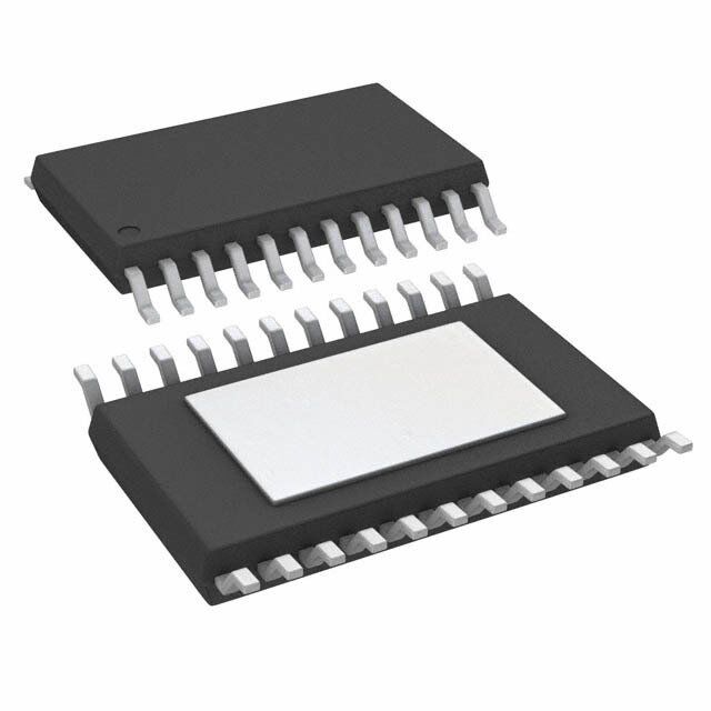
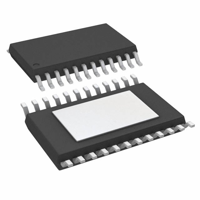
| 产品图片 |
|
| rohs | 符合RoHS无铅 / 符合限制有害物质指令(RoHS)规范要求 |
| 产品系列 | 音频 IC,音频放大器,Texas Instruments TPA6013A4PWP- |
| 数据手册 | |
| 产品型号 | TPA6013A4PWP |
| PCN组件/产地 | |
| THD+噪声 | 0.03 % |
| 不同负载时的最大输出功率x通道数 | 3.2W x 2 @ 3 欧姆; 235mW x 2 @ 16 欧姆 |
| 产品 | Class-AB |
| 产品种类 | 音频放大器 |
| 供应商器件封装 | 24-HTSSOP |
| 其它名称 | 296-34556-5 |
| 包装 | 管件 |
| 商标 | Texas Instruments |
| 安装类型 | 表面贴装 |
| 安装风格 | SMD/SMT |
| 封装 | Tube |
| 封装/外壳 | 24-TSSOP(0.173",4.40mm 宽)裸焊盘 |
| 封装/箱体 | HTSSOP-24 |
| 工作温度 | -40°C ~ 85°C (TA) |
| 工作电源电压 | 4 V to 5.5 V |
| 工厂包装数量 | 60 |
| 最大工作温度 | + 85 C |
| 最小工作温度 | - 40 C |
| 标准包装 | 60 |
| 特性 | 差分输入,输入多路复用器,音量衰减,关机,热保护,音量控制 |
| 电压-电源 | 4 V ~ 5.5 V |
| 电源电压-最大 | 5.5 V |
| 电源电压-最小 | 4 V |
| 电源电流 | 6.7 mA |
| 类型 | AB 类 |
| 系列 | TPA6013A4 |
| 输入信号类型 | Differential |
| 输出功率 | 3 W |
| 输出类型 | 2-通道(立体声)带立体声耳机 |


- 商务部:美国ITC正式对集成电路等产品启动337调查
- 曝三星4nm工艺存在良率问题 高通将骁龙8 Gen1或转产台积电
- 太阳诱电将投资9.5亿元在常州建新厂生产MLCC 预计2023年完工
- 英特尔发布欧洲新工厂建设计划 深化IDM 2.0 战略
- 台积电先进制程称霸业界 有大客户加持明年业绩稳了
- 达到5530亿美元!SIA预计今年全球半导体销售额将创下新高
- 英特尔拟将自动驾驶子公司Mobileye上市 估值或超500亿美元
- 三星加码芯片和SET,合并消费电子和移动部门,撤换高东真等 CEO
- 三星电子宣布重大人事变动 还合并消费电子和移动部门
- 海关总署:前11个月进口集成电路产品价值2.52万亿元 增长14.8%


PDF Datasheet 数据手册内容提取
TPA6013A4 www.ti.com SLOS635–NOVEMBER2009 3-W STEREO AUDIO POWER AMPLIFIER WITH ADVANCED DC VOLUME CONTROL CheckforSamples:TPA6013A4 FEATURES 1 DESCRIPTION • Advanced32-StepsDCVolumeControl 2 – Stepsfrom –40to18dB The TPA6013A4 is a stereo audio power amplifier that drives 3 W/channel of continuous RMS power – FadeMode into a 3-Ω load. Advanced dc volume control – MaximumVolumeSettingforSEMode minimizes external components and allows BTL – AdjustableSEVolumeControl (speaker) volume control and SE (headphone) ReferencedtoBTLVolumeControl volume control. Notebook and pocket PCs benefit from the integrated feature set that minimizes • 3WInto3-Ω Speakers externalcomponentswithoutsacrificingfunctionality. • StereoInputMUX To simplify design, the speaker volume level is • HeadphoneMode adjusted by applying a dc voltage to the VOLUME • Pin-to-pincompatiblewithTPA6011A4and terminal. Likewise, the delta between speaker volume TPA6012A4 and headphone volume can be adjusted by applying • 24-pinPowerPAD™Package(PWP) a dc voltage to the SEDIFF terminal. To avoid an unexpected high volume level through the APPLICATIONS headphones, a third terminal, SEMAX, limits the headphone volume level when a dc voltage is • NotebookPC applied. Finally, to ensure a smooth transition • LCDMonitors between active and shutdown modes, a fade mode • PocketPC rampsthevolumeupanddown. APPLICATION CIRCUIT DC VOLUME CONTROL Right GAIN (BTL) Speaker vs 1 ROUT+ 24 VDD CC VOLUME VOLTAGE PGND SE/BTL 23 100 kW 20 Volume Up CS 2 ROUT− 10 Volume Down 3 HP/LINE 22 100 kW 1 kW 0 Power Supply PVDD −10 Ci AAuudRdioiioRg S hiSgotoh uLutr inrHcceePe Ci Ci 564 RRHLIPNIENIN VSOELDUIMFEF 122901 PI(nDo tCFer noVtomioorl mtDaegAteCe)r Gain−dB −−−432000 CS VDD RIN SEMAX −50 7 18 Headphones −60 Ci 8 VDD AGND 17 C(BYP) −70 VDD= 5.0 V LIN BYPASS −80 BTL Output AudioL eSfot uLrincee Ci Ci 9 LLINEIN FADE 16 CC 1 kW −900.0 0.5 1.0 1.5 2.0 2.5 3.0 3.5 4R.L0= N4o. 5Load5.0 Audio LSeofut rHcPe 10 LHPIN SHUTDOWN 15 System Control Volume [Pin 21]−V Power Supply 11 PVDD LOUT+ 14 Left CS 12 LOUT− PGND 13 Speaker S001 Figure1. ApplicationCircuitandDCVolumeControl 1 Pleasebeawarethatanimportantnoticeconcerningavailability,standardwarranty,anduseincriticalapplicationsofTexas Instrumentssemiconductorproductsanddisclaimerstheretoappearsattheendofthisdatasheet. PowerPADisatrademarkofTexasInstruments. 2 PRODUCTIONDATAinformationiscurrentasofpublicationdate. Copyright©2009,TexasInstrumentsIncorporated Products conform to specifications per the terms of the Texas Instruments standard warranty. Production processing does not necessarilyincludetestingofallparameters.
TPA6013A4 SLOS635–NOVEMBER2009 www.ti.com This integrated circuit can be damaged by ESD. Texas Instruments recommends that all integrated circuits be handled with appropriateprecautions.Failuretoobserveproperhandlingandinstallationprocedurescancausedamage. ESDdamagecanrangefromsubtleperformancedegradationtocompletedevicefailure.Precisionintegratedcircuitsmaybemore susceptibletodamagebecauseverysmallparametricchangescouldcausethedevicenottomeetitspublishedspecifications. AVAILABLEOPTIONS PACKAGE T A 24-PINTSSOP(PWP) (1) –40°Cto85°C TPA6013A4PWP (1) ThePWPpackageisavailabletapedandreeled.Toorderataped andreeledpart,addthesuffixRtothepartnumber (e.g.,TPA6013A4PWPR). LEAD(PB-FREE)ORDERINGINFORMATION ORDERABLEDEVICE STATUS (1) ECO-STATUS (2) TPA6013A4PWPG4 Active Pb-Free TPA6013A4PWPRG4 Active andGreen (1) Themarketingstatusvaluesaredefinedasfollows: (a) ACTIVE:Thisdevicerecommendedfornewdesigns. (b) LIFEBUY:TIhasannouncedthatthedevicewillbediscontinued,andalifetime-buyperiodisineffect. (c) NRND:Notrecommendedfornewdesigns.Deviceisinproductiontosupportexistingcustomers,butTIdoesnotrecommendusing thispartinanewdesign. (d) PREVIEW:Devicehasbeenannouncedbutisnotinproduction.Samplesmayormaynotbeavailable. (e) OBSOLETE:TIhasdiscontinuedproductionofthedevice. (2) Eco-StatusInformation–Additionaldetailsincludingspecificmaterialcontentcanbeaccessedatwww.ti.com/leadfree (a) N/A:NotyetavailableLead(Pb)-Free,forestimatedconversiondatesgotowww.ti.com/leadfree. (b) Pb-Free:TIdefines"Lead(Pb)-Free"or"Pb-Free"tomeanRoHScompatible,includingaleadconcentrationthatdoesnotexceed 0.1%oftotalproductweight,and,ifdesignedtobesoldered,suitableforuseinspecifiedlead-freesolderingprocesses. (c) Green:TIdevices"Green"tomeanLead(Pb)-Freeandinaddition,usespackagematerialsthatdonotcontainhalogens,including bromine(Br),orantimony(Sb)above0.1%oftotalproductweight. ABSOLUTE MAXIMUM RATINGS overoperatingfree-airtemperaturerange(unlessotherwisenoted)(1) UNIT V Supplyvoltage,V ,PV –0.3Vto6V SS DD DD V Inputvoltage –0.3VtoV +0.3V I DD Continuoustotalpowerdissipation SeeDissipationRatingTable T Operatingfree-airtemperaturerange –40°Cto85°C A T Operatingjunctiontemperaturerange –40°Cto150°C J T Storagetemperaturerange –65°Cto150°C stg (1) Stressesbeyondthoselistedunder"absolutemaximumratings"maycausepermanentdamagetothedevice.Thesearestressratings only,andfunctionaloperationofthedeviceattheseoranyotherconditionsbeyondthoseindicatedunder"recommendedoperating conditions"isnotimplied.Exposuretoabsolute-maximum-ratedconditionsforextendedperiodsmayaffectdevicereliability. DISSIPATION RATING TABLE T ≤25°C DERATINGFACTOR T =70°C T =85°C PACKAGE A A A POWERRATING ABOVET =25°C POWERRATING POWERRATING A PWP 2.7mW 21.8mW/°C 1.7W 1.4W 2 SubmitDocumentationFeedback Copyright©2009,TexasInstrumentsIncorporated ProductFolderLink(s):TPA6013A4
TPA6013A4 www.ti.com SLOS635–NOVEMBER2009 RECOMMENDED OPERATING CONDITIONS MIN MAX UNIT V Supplyvoltage,V ,PV 4.0 5.5 V SS DD DD SE/BTL,HP/LINE,FADE 0.8×V V DD V High-levelinputvoltage IH SHUTDOWN 2 V SE/BTL,HP/LINE,FADE 0.6×V V DD V Low-levelinputvoltage IL SHUTDOWN 0.8 V T Operatingfree-airtemperature –40 85 °C A ELECTRICAL CHARACTERISTICS T =25°C,V =PV =5.5V(unlessotherwisenoted) A DD DD PARAMETER TESTCONDITIONS MIN TYP MAX UNIT V =5.5V,Gain=0dB,SE/BTL=0V 2 30 mV DD |V | Outputoffsetvoltage(measureddifferentially) OO V =5.5V,Gain=18dB,SE/BTL=0V 2.6 50 mV DD PSRR Powersupplyrejectionratio V =PV =4.0Vto5.5V,Gain=0dB –80 dB DD DD High-levelinputcurrent(SE/BTL,FADE,HP/LINE, V =PV =5.5V, |I | DD DD 1 μA IH SHUTDOWN,SEDIFF,SEMAX,VOLUME) V =V =PV I DD DD Low-levelinputcurrent(SE/BTL,FADE,HP/LINE, |I | V =PV =5.5V,V =0V 1 μA IL SHUTDOWN,SEDIFF,SEMAX,VOLUME) DD DD I V =PV =5V,SE/BTL=0V, DD DD 6.7 9.0 SHUTDOWN=2V I Supplycurrent,noload mA DD V =PV =5V,SE/BTL=5V, DD DD 4.5 6 SHUTDOWN=2V V =5V=PV ,SE/BTL=0V, DD DD I Supplycurrent,maxpowerintoa3-Ωload SHUTDOWN=2V,R =3Ω, 1.5 A DD L RMS P =2W,stereo O I Supplycurrent,shutdownmode SHUTDOWN=0.0V 10 25 μA DD(SD) OPERATING CHARACTERISTICS T =25°C,V =PV =5V,R =3Ω,Gain=6dB,Stereo(unlessotherwisenoted) A DD DD L PARAMETER TESTCONDITIONS MIN TYP MAX UNIT THD=1%,f=1kHz,R =16Ω(SE) 195 mW L THD=10%,f=1kHz,R =16Ω(SE) 235 mW L P Outputpower O THD=1%,f=1kHz,R =3Ω(BTL) 2.0 L W THD=10%,f=1kHz,V =5.5V,R =3Ω(BTL) 3.2 DD L THD+N Totalharmonicdistortion+noise P =0.9W,R =8Ω(BTL),f=20Hzto20kHz <0.1% O L P =0.1W,R =16Ω(SE),f=20Hzto20kHz 0.03% O L V High-leveloutputvoltage R =8Ω,MeasuredbetweenoutputandV =5.5V 700 mV OH L DD R =8Ω,MeasuredbetweenoutputandGND, V Low-leveloutputvoltage L 400 mV OL V =5.5V DD V Bypassvoltage(NominallyV /2) Measuredatpin17,Noload,V =5.5V 2.65 2.75 2.85 V (Bypass) DD DD BTL(4Ω) –66 dB Supplyripplerejectionratio f=1kHz,Gain=0dB,C =1µF (BYP) SE(32Ω) –60 dB BTL 110 dB Crosstalk SE 102 dB f=20Hzto20kHz,Gain=0dB, Noiseoutputvoltage BTL 36 µV C =1µF RMS (BYP) Z Inputimpedance(seeFigure17) VOLUME=5V 12 kΩ I Copyright©2009,TexasInstrumentsIncorporated SubmitDocumentationFeedback 3 ProductFolderLink(s):TPA6013A4
TPA6013A4 SLOS635–NOVEMBER2009 www.ti.com PWPPackage (Top View) PGND 1 24 ROUT+ ROUT− 2 23 SE/BTL PVDD 3 22 HP/LINE RHPIN 4 21 VOLUME RLINEIN 5 20 SEDIFF RIN 6 19 SEMAX VDD 7 18 AGND LIN 8 17 BYPASS LLINEIN 9 16 FADE LHPIN 10 15 SHUTDOWN PVDD 11 14 LOUT+ LOUT− 12 13 PGND P0110-01 PINFunctions PIN I/O DESCRIPTION NAME NO. PGND 1,13 – Powerground LOUT– 12 O Leftchannelnegativeaudiooutput PV 3,11 – Supplyvoltageterminalforpowerstage DD LHPIN 10 I Leftchannelheadphoneinput,selectedwhenHP/LINEisheldhigh LLINEIN 9 I Leftchannellineinput,selectedwhenHP/LINEisheldlow LIN 8 I Commonleftchannelinputforfullydifferentialinput.ACgroundforsingle-endedinputs. V 7 – Supplyvoltageterminal DD RIN 6 I Commonrightchannelinputforfullydifferentialinput.ACgroundforsingle-endedinputs. RLINEIN 5 I Rightchannellineinput,selectedwhenHP/LINEisheldlow RHPIN 4 I Rightchannelheadphoneinput,selectedwhenHP/LINEisheldhigh ROUT– 2 O Rightchannelnegativeaudiooutput ROUT+ 24 O Rightchannelpositiveaudiooutput SHUTDOWN 15 I PlacestheamplifierinshutdownmodeifaTTLlogiclowisplacedonthisterminal Placestheamplifierinfademodeifalogiclowisplacedonthisterminal;normaloperationifalogic FADE 16 I highisplacedonthisterminal BYPASS 17 I Taptovoltagedividerforinternalmid-supplybiasgeneratorusedforanalogreference AGND 18 – Analogpowersupplyground SEMAX 19 I Setsthemaximumvolumeforsingleendedoperation.DCvoltagerangeis0toV . DD SEDIFF 20 I SetsthedifferencebetweenBTLvolumeandSEvolume.DCvoltagerangeis0toV . DD VOLUME 21 I Terminalfordcvolumecontrol.DCvoltagerangeis0toV . DD InputMUXcontrol.Whenlogichigh,RHPINandLHPINinputsareselected.Whenlogiclow,RLINEIN HP/LINE 22 I andLLINEINinputsareselected. OutputMUXcontrol.Whenthisterminalishigh,SEoutputsareselected.Whenthisterminalislow, SE/BTL 23 I BTLoutputsareselected. LOUT+ 14 O Leftchannelpositiveaudiooutput. 4 SubmitDocumentationFeedback Copyright©2009,TexasInstrumentsIncorporated ProductFolderLink(s):TPA6013A4
TPA6013A4 www.ti.com SLOS635–NOVEMBER2009 FUNCTIONAL BLOCK DIAGRAM RHPIN R MUX RLINEIN _ _ HP/LINE + ROUT+ + RIN BYP BYP + _ _ ROUT- + EN BYP SE/BTL SE/BTL MUX HP/LINE Control PVDD PGND VDD VOLUME Power 32-Step Management BYPASS SEDIFF Volume SEMAX Control SHUTDOWN FADE AGND LHPIN L MUX LLINEIN _ _ HP/LINE + LOUT+ + LIN BYP BYP + _ _ LOUT- + EN BYP SE/BTL NOTE: Allresistorwipersareadjustedwith32-stepvolumecontrol. Copyright©2009,TexasInstrumentsIncorporated SubmitDocumentationFeedback 5 ProductFolderLink(s):TPA6013A4
TPA6013A4 SLOS635–NOVEMBER2009 www.ti.com Table1.DCVolumeControl(BTLMode,V =5V)(1) DD VOLUME(PIN21) GAINOFAMPLIFIER FROM(V) TO(V) (Typ) (2) 0.00 0.26 –85 0.33 0.37 –40 0.44 0.48 –34 0.56 0.59 –31 0.67 0.70 –28 0.78 0.82 –25 0.89 0.93 –22 1.01 1.04 –19 1.12 1.16 –16 1.23 1.27 –13 1.35 1.38 –10 1.46 1.49 –7 1.57 1.60 –4 1.68 1.72 –2 1.79 1.83 –0 1.91 1.94 2 2.02 2.06 4 2.13 2.17 6 2.25 2.28 8 2.36 2.39 10 2.47 2.50 11 2.58 2.61 12 2.70 2.73 13 2.81 2.83 14 2.92 2.95 14.5 3.04 3.06 15 3.15 3.17 15.5 3.26 3.29 16 3.38 3.40 16.5 3.49 3.51 17 3.60 3.63 17.5 3.71 5.00 18 (1) ForothervaluesofV ,scalethevoltagevaluesinthetablebyafactorofV /5. DD DD (2) Testedinproduction.Remaininggainstepsarespecifiedbydesign. 6 SubmitDocumentationFeedback Copyright©2009,TexasInstrumentsIncorporated ProductFolderLink(s):TPA6013A4
TPA6013A4 www.ti.com SLOS635–NOVEMBER2009 Table2.DCVolumeControl(SEMode,V =5V)(1) DD SE_VOLUME=VOLUME-SEDIFForSEMAX GAINOFAMPLIFIER FROM(V) TO(V) (Typ) 0.00 0.26 –85(2) 0.33 0.37 –46 0.44 0.48 –40 0.56 0.59 –37 0.67 0.70 –34 0.78 0.82 –31 0.89 0.93 –28 1.01 1.04 –25 1.12 1.16 –22 1.23 1.27 –19 1.35 1.38 –16 1.46 1.49 –13 1.57 1.60 –10 1.68 1.72 –8 1.79 1.83 –6(2) 1.91 1.94 –4 2.02 2.06 –2 2.13 2.17 0(2) 2.25 2.28 2 2.36 2.39 4 2.47 2.50 5 2.58 2.61 6 (2) 2.70 2.73 7 2.81 2.83 8 2.92 2.95 8.5 3.04 3.06 9 3.15 3.17 9.5 3.26 3.29 10 3.38 3.40 10.5 3.49 3.51 11 3.60 3.63 11.5 3.71 5.00 12 (1) ForothervaluesofV ,scalethevoltagevaluesinthetablebyafactorofV /5. DD DD (2) Testedinproduction.Remaininggainstepsarespecifiedbydesign. Copyright©2009,TexasInstrumentsIncorporated SubmitDocumentationFeedback 7 ProductFolderLink(s):TPA6013A4
TPA6013A4 SLOS635–NOVEMBER2009 www.ti.com TYPICAL CHARACTERISTICS Testconditions(unlessotherwisenoted)fortypicaloperatingperformance: V =5.0V,C =1µF,C =1µF,T =27°C,SHUTDOWN=V DD IN BYPASS A DD Table of Graphs Gain(BTL) vsVolumevoltage Figure1 vsFrequency Figure2,Figure3,Figure4 THD+N Totalharmonicdistortionplusnoise(BTL) vsOutputpower Figure7,Figure8,Figure9 vsFrequency Figure5,Figure6 THD+N Totalharmonicdistortionplusnoise(SE) vsOutputpower Figure10 vsOutputvoltage Figure11 P Totalpowerdissipation(BTL) vsTotaloutputpower Figure12 D P Totalpowerdissipation(SE) vsTotaloutputpower Figure13 D Crosstalk(BTL) vsFrequency Figure14 Crosstalk(SE) vsFrequency Figure15 Inter-channelcrosstalk vsFrequency Figure16 Inputimpedance vsGain Figure17 PSRR Powersupplyrejectionratio(BTL) vsFrequency Figure18 PSRR Powersupplyrejectionratio(SE) vsFrequency Figure19 I Supplycurrent(BTL) vsTotaloutputpower Figure20 DD I Supplycurrent(SE) vsTotaloutputpower Figure21 DD TOTALHARMONICDISTORTION+NOISE(BTL) TOTALHARMONICDISTORTION+NOISE(BTL) vs vs FREQUENCY FREQUENCY % 10 % 10 − VDD = 5.0 V PO = 500 mW − VDD = 5.0 V PO = 250 mW Noise RLILN =E I3N W Input − BTL Output PPOO == 11 .W5 W Noise RLILN =E I4N W Input − BTL Output PPOO == 11 .W5 W n + 1 Gain = 6 dB n + 1 Gain = 6 dB o o orti orti Dist Dist nic 0.1 nic 0.1 o o m m ar ar H H al al ot 0.01 ot 0.01 T T − − N N + + D D H H T 0.001 T 0.001 20 100 1k 10k 20k 20 100 1k 10k 20k f − Frequency − Hz f − Frequency − Hz Figure2. Figure3. 8 SubmitDocumentationFeedback Copyright©2009,TexasInstrumentsIncorporated ProductFolderLink(s):TPA6013A4
TPA6013A4 www.ti.com SLOS635–NOVEMBER2009 TOTALHARMONICDISTORTION+NOISE(BTL) TOTALHARMONICDISTORTION+NOISE(SE) vs vs FREQUENCY FREQUENCY % 10 % 10 − VDD = 5.0 V PO = 250 mW − VDD = 5.0 V PO = 10 mW Noise RLILN =E I8N W Input − BTL Output PPOO == 590000 mmWW Noise RHLP I=N 3 I2n pWut − SE Output PPOO == 4800 mmWW n + 1 Gain = 6 dB n + 1 Gain = 0 dB o o orti orti Dist Dist nic 0.1 nic 0.1 o o m m ar ar H H al al ot 0.01 ot 0.01 T T − − N N + + D D H H T 0.001 T 0.001 20 100 1k 10k 20k 20 100 1k 10k 20k f − Frequency − Hz f − Frequency − Hz Figure4. Figure5. TOTALHARMONICDISTORTION+NOISE(SE) TOTALHARMONICDISTORTION+NOISE(BTL) vs vs FREQUENCY OUTPUTPOWER − % 10 VDD = 5.0 V VO = 500 mVRMS − % 100 RL = 3 W VDD = 4.5 V Noise RHLP I=N 1 I0n pkuWt − SE Output VVOO == 11..07 5V VRMRSMS Noise LGIaNiEn I=N 6In dpBut − BTL Output VVDDDD == 55..05 VV n + 1 Gain = 0 dB n + 10 o o orti orti Dist Dist nic 0.1 nic 1 o o m m ar ar H H al al ot 0.01 ot 0.1 T T − − N N + + D D H H T 0.001 T 0.01 20 100 1k 10k 20k 1m 10m 100m 1 4 f − Frequency − Hz PO − Output Power − W Figure6. Figure7. TOTALHARMONICDISTORTION+NOISE(BTL) TOTALHARMONICDISTORTION+NOISE(BTL) vs vs OUTPUTPOWER OUTPUTPOWER − % 100 RL = 4 W VDD = 4.5 V − % 100 RL = 8 W VDD = 4.5 V Noise LGIaNiEn I=N 6In dpBut − BTL Output VVDDDD == 55..05 VV Noise LGIaNiEn I=N 6In dpBut − BTL Output VVDDDD == 55..05 VV n + 10 n + 10 o o orti orti Dist Dist nic 1 nic 1 o o m m ar ar H H al al ot 0.1 ot 0.1 T T − − N N + + D D H H T 0.01 T 0.01 1m 10m 100m 1 3 1m 10m 100m 1 2 PO − Output Power − W PO − Output Power − W Figure8. Figure9. Copyright©2009,TexasInstrumentsIncorporated SubmitDocumentationFeedback 9 ProductFolderLink(s):TPA6013A4
TPA6013A4 SLOS635–NOVEMBER2009 www.ti.com TOTALHARMONICDISTORTION+NOISE(SE) TOTALHARMONICDISTORTION+NOISE(SE) vs vs OUTPUTPOWER OUTPUTVOLTAGE − % 100 VDD = 5.0 V RL = 16 W − % 100 VDD = 5.0 V oise HGPaiInN =In 0p udtB − SE Output RL = 32 W oise RHLP I=N 1 I0n pkuWt − SE Output N N 10 n + 10 n + Gain = 0 dB o o orti orti Dist Dist 1 nic 1 nic o o arm arm 0.1 H H al al ot 0.1 ot − T − T 0.01 N N + + D D H H T 0.01 T 0.001 100u 1m 10m 100m 300m 0.0 500.0m 1.0 1.5 2.0 PO − Output Power − W VO − Output Voltage − VRMS Figure10. Figure11. TOTALPOWERDISSIPATION(BTL) TOTALPOWERDISSIPATION(SE) vs vs TOTALOUTPUTPOWER TOTALOUTPUTPOWER 4.0 200m VDD = 5.0 V VDD = 5.0 V 3.5 LINEIN Input 175m HPIN Input W BTL Output W SE Output Dissipation − 23..50 Gain = 6 dB Dissipation − 112550mm Gain = 0 dB wer 2.0 wer 100m P − Total PoD 011...505 RRRLLL === 348 WWW P − Total PoD 257505mmm RRLL == 1362 WW 0.0 0 0.0 0.5 1.0 1.5 2.0 2.5 3.0 3.5 4.0 4.5 5.0 0 100m 200m 300m 400m 500m PO − Total Output Power − W PO − Total Output Power − W Figure12. Figure13. CROSSTALK(BTL) CROSSTALK(SE) vs vs FREQUENCY FREQUENCY 0 0 RL = 4 W RL = 32 W −20 PLION =E I1N W Input − BTL Output −20 PHOP I=N 5 I0n pmuWt − SE Output Gain = 6 dB Gain = 0 dB −40 −40 B B d d − −60 − −60 alk alk osst −80 osst −80 Cr Cr −100 −100 −120 −120 −140 −140 20 100 1k 10k 20k 20 100 1k 10k 20k f − Frequency − Hz f − Frequency − Hz Figure14. Figure15. 10 SubmitDocumentationFeedback Copyright©2009,TexasInstrumentsIncorporated ProductFolderLink(s):TPA6013A4
TPA6013A4 www.ti.com SLOS635–NOVEMBER2009 INTER-CHANNELCROSSTALK INPUTIMPEDANCE vs vs FREQUENCY GAIN 0 120k VDD = 5.0 V Line Active Differential RL = 4 W HP Active Single−Ended −20 VIN = 1 VRMS − BTL Output 100k dB Gain = 18 dB − el Crosstalk −−6400 Wpedance − 6800kk n m Chan −80 put I 40k er− In nt I −100 20k VDD = 5.0 V RL = No Load −120 0 20 100 1k 10k 20k −40 −35 −30 −25 −20 −15 −10 −5 0 5 10 15 20 f − Frequency − Hz Gain − dB Figure16. Figure17. POWERSUPPLYREJECTIONRATIO(BTL) POWERSUPPLYREJECTIONRATIO(SE) vs vs FREQUENCY FREQUENCY 0 0 B VDD = 5.0 V Gain = 6 dB B VDD = 5.0 V Gain = 0 dB − d RL = 4 W Gain = 18 dB − d RL = 32 W Gain = 12 dB o BTL Output o SE Output Rati −20 Supply Ripple = 0.2 Vpp Sine Wave Rati −20 Supply Ripple = 0.2 Vpp Sine Wave n n o o ecti ecti ej ej R R ply −40 ply −40 p p u u S S er er w w Po −60 Po −60 − − R R R R S S P P −80 −80 20 100 1k 10k 20k 20 100 1k 10k 20k f − Frequency − Hz f − Frequency − Hz Figure18. Figure19. SUPPLYCURRENT(BTL) SUPPLYCURRENT(SE) vs vs TOTALOUTPUTPOWER TOTALOUTPUTPOWER 1.8 125m VDD = 5.0 V VDD = 5.0 V 1.6 LINEIN Input HPIN Input BTL Output SE Output 1.4 Gain = 6 dB 100m Gain = 0 dB A A nt − 1.2 nt − urre 1.0 urre 75m C C ply 0.8 ply up up 50m S S − 0.6 − I DD 0.4 RL = 3 W I DD 25m 0.2 RL = 4 W RL = 16 W RL = 8 W RL = 32 W 0.0 0 0.0 0.5 1.0 1.5 2.0 2.5 3.0 3.5 4.0 4.5 5.0 0 100m 200m 300m 400m 500m PO − Total Output Power − W PO − Total Output Power − W Figure20. Figure21. Copyright©2009,TexasInstrumentsIncorporated SubmitDocumentationFeedback 11 ProductFolderLink(s):TPA6013A4
TPA6013A4 SLOS635–NOVEMBER2009 www.ti.com APPLICATION INFORMATION SELECTION OF COMPONENTS Figure22andFigure23areschematicdiagramsoftypicalnotebookcomputerapplicationcircuits. Right Speaker 24 VDD ROUT+ CC 1 PGND SE/BTL 23 100 kW 2 CS ROUT- 22 100 kW 3 HP/LINE 1 kW Power Supply PVDD Ci Right HP 4 21 RHPIN VOLUME Audio Source Ci In From DAC Right Line 5 20 or RLINEIN SEDIFF Audio Source Potentiometer Ci (DC Voltage) 6 19 RIN SEMAX CS VDD 7 18 Headphones VDD AGND Ci C(BYP) 8 17 LIN BYPASS 1 kW Ci CC Left Line 9 16 Audio Source LLINEIN FADE Ci Left HP 10 15 System LHPIN Audio Source SHUTDOWN Control Power Supply 11 PVDD LOUT+ 14 Left 12 13 Speaker CS LOUT- PGND A. A 0.1-μF ceramic capacitor should be placed as close as possible to the IC. For filtering lower-frequency noise signals,alargerelectrolyticcapacitorof10μForgreatershouldbeplacedneartheaudiopoweramplifier. Figure22. TypicalTPA6013A4ApplicationCircuitUsingSingle-EndedInputsandInputMUX 12 SubmitDocumentationFeedback Copyright©2009,TexasInstrumentsIncorporated ProductFolderLink(s):TPA6013A4
TPA6013A4 www.ti.com SLOS635–NOVEMBER2009 Right Speaker 24 VDD ROUT+ CC 1 PGND SE/BTL 23 100 kW 2 CS ROUT- 22 100 kW 3 HP/LINE 1 kW Power Supply PVDD 4 21 NC RHPIN VOLUME Ci In From DAC Right Negative 5 20 or RLINEIN SEDIFF Differential Input Signal Potentiometer Ci (DC Voltage) Right Positive 6 19 RIN SEMAX Differential Input Signal CS VDD 7 18 Headphones VDD AGND Ci C(BYP) 8 17 Left Positive Differential LIN BYPASS Input Signal 1 kW Ci CC Left Negative 9 16 Differential Input Signal LLINEIN FADE 10 15 System NC LHPIN SHUTDOWN Control Power Supply 11 PVDD LOUT+ 14 Left 12 13 Speaker CS LOUT- PGND A. A 0.1-μF ceramic capacitor should be placed as close as possible to the IC. For filtering lower-frequency noise signals,alargerelectrolyticcapacitorof10μForgreatershouldbeplacedneartheaudiopoweramplifier. Figure23. TypicalTPA6013A4ApplicationCircuitUsingDifferentialInputs SE/BTL OPERATION The ability of the TPA6013A4 to easily switch between BTL and SE modes is one of its most important cost saving features. This feature eliminates the requirement for an additional headphone amplifier in applications where internal stereo speakers are driven in BTL mode but external headphone or speakers must be accommodated. Internal to the TPA6013A4, two separate amplifiers drive OUT+ and OUT–. The SE/BTL input controls the operation of the follower amplifier that drives LOUT– and ROUT–. When SE/BTL is held low, the amplifier is on and the TPA6013A4 is in the BTL mode. When SE/BTL is held high, the OUT– amplifiers are in a high output impedance state, which configures the TPA6013A4 as an SE driver from LOUT+ and ROUT+. I is DD reduced by approximately one-third in SE mode. Control of the SE/BTL input can be from a logic-level CMOS source or, more typically, from a resistor divider network as shown in Figure 24. The trip level for the SE/BTL inputcanbefoundintherecommendedoperatingconditionstable. Copyright©2009,TexasInstrumentsIncorporated SubmitDocumentationFeedback 13 ProductFolderLink(s):TPA6013A4
TPA6013A4 SLOS635–NOVEMBER2009 www.ti.com 4 RHPIN R MUX 5 RLINEIN _ _ ROUT+ 24 + 22 HP/LINE Input + MUX Bypass Control 6 RIN Bypass VDD C33O0 m F + _ _ ROUT- 2 1 kW + 100 kW EN Bypass 100 kW SE/BTL 23 LOUT+ Figure24. TPA6013A4ResistorDividerNetworkCircuit Using a 1/8-in. (3,5 mm) stereo headphone jack, the control switch is closed when no plug is inserted. When closed the 100-kΩ/1-kΩ divider pulls the SE/BTL input low. When a plug is inserted, the 1-kΩ resistor is disconnected and the SE/BTL input is pulled high. When the input goes high, the OUT– amplifier is shut down causing the speaker to mute (open-circuits the speaker). The OUT+ amplifier then drives through the output capacitor(C )intotheheadphonejack. o HP/LINE OPERATION The HP/LINE input controls the internal input multiplexer (MUX). Refer to the block diagram in Figure 24. This allows the device to switch between two separate stereo inputs to the amplifier. For design flexibility, the HP/LINE control is independent of the output mode, SE or BTL, which is controlled by the aforementioned SE/BTLpin.ToallowtheamplifiertoswitchfromtheLINEinputstotheHPinputswhentheoutputswitchesfrom BTLmodetoSEmode,simplyconnecttheSE/BTLcontrolinputtotheHP/LINEinput. When this input is logic high, the RHPIN and LHPIN inputs are selected. When this terminal is logic low, the RLINEINandLLINEINinputsareselected.ThisoperationisalsodetailedinTable3andthetriplevelsforalogic low(V )orlogichigh(V )canbefoundintherecommendedoperatingconditionstable. IL IH SHUTDOWN MODES The TPA6013A4 employs a shutdown mode of operation designed to reduce supply current (I ) to the absolute DD minimum level during periods of nonuse for battery-power conservation. The SHUTDOWN input terminal should beheldhighduringnormaloperationwhentheamplifierisinuse.PullingSHUTDOWNlowcausestheoutputsto mute and the amplifier to enter a low-current state, I = 20 μA. SHUTDOWN should never be left unconnected DD becauseamplifieroperationwouldbeunpredictable. 14 SubmitDocumentationFeedback Copyright©2009,TexasInstrumentsIncorporated ProductFolderLink(s):TPA6013A4
TPA6013A4 www.ti.com SLOS635–NOVEMBER2009 Table3.HP/LINE,SE/BTL,andShutdownFunctions INPUTS (1) AMPLIFIERSTATE HP/LINE SE/BTL SHUTDOWN INPUT OUTPUT X X Low X Mute Low Low High Line BTL Low High High Line SE High Low High HP BTL High High High HP SE (1) Inputsshouldneverbeleftunconnected. FADE OPERATION For design flexibility, a fade mode is provided to slowly ramp up the amplifier gain when coming out of shutdown mode and conversely ramp the gain down when going into shutdown. This mode provides a smooth transition betweentheactiveandshutdownstatesandvirtuallyeliminatesanypopsorclicksontheoutputs. When the FADE input is a logic low, the device is placed into fade-on mode. A logic high on this pin places the amplifier in the fade-off mode. The voltage trip levels for a logic low (V ) or logic high (V ) can be found in the IL IH recommendedoperatingconditionstable. When a logic low is applied to the FADE pin and a logic low is then applied on the SHUTDOWNpin, the channel gain steps down from gain step to gain step at a rate of two clock cycles per step. With a nominal internal clock frequency of 58 Hz, this equates to 34 ms (1/24 Hz) per step. The gain steps down until the lowest gain step is reached. The time it takes to reach this step depends on the gain setting prior to placing the device in shutdown. For example, if the amplifier is in the highest gain mode of 18 dB, the time it takes to ramp down the channel gain is 1.05 seconds. This number is calculated by taking the number of steps to reach the lowest gain from the highestgain,or31steps,andmultiplyingbythetimeperstep,or34ms. After the channel gain is stepped down to the lowest gain, the amplifier begins discharging the bypass capacitor from the nominal voltage of V /2 to ground. This time is dependent on the value of the bypass capacitor. For a DD 0.47-μF capacitor that is used in the application diagram in Figure 22, the time is approximately 500 ms. This time scales linearly with the value of bypass capacitor. For example, if a 1-μF capacitor is used for bypass, the timeperiodtodischargethecapacitortogroundistwicethatofthe0.47-μFcapacitor,or1second.Figure25 isa waveform captured at the output during the shutdown sequence when the part is in fade-on mode. The gain is settothehighestlevelandtheoutputisatV whentheamplifierisshutdown. DD When a logic high is placed on the SHUTDOWN pin and the FADE pin is still held low, the device begins the start-up process. The bypass capacitor will begin charging. Once the bypass voltage reaches the final value of V /2, the gain increases from the lowest gain level to the gain level set by the dc voltage applied to the DD VOLUME,SEDIFF,andSEMAXpins. In the fade-off mode, the amplifier stores the gain value prior to starting the shutdown sequence. The output of the amplifier immediately drops to V /2 and the bypass capacitor begins a smooth discharge to ground. When DD shutdown is released, the bypass capacitor charges up to V /2 and the channel gain returns immediately to the DD valuestoredinmemory.Figure26isawaveformcapturedattheoutputduringtheshutdownsequencewhenthe part is in the fade-off mode. The gain is set to the highest level, and the output is at V when the amplifier is DD shutdown. The power-up sequence is different from the shutdown sequence and the voltage on the FADEpin does not change the power-up sequence. Upon a power-up condition, the TPA6013A4 begins in the lowest gain setting and steps up every 2 clock cycles until the final value is reached as determined by the dc voltage applied to the VOLUME,SEDIFF,andSEMAXpins. Copyright©2009,TexasInstrumentsIncorporated SubmitDocumentationFeedback 15 ProductFolderLink(s):TPA6013A4
TPA6013A4 SLOS635–NOVEMBER2009 www.ti.com Device Shutdown Device Shutdown ROUT+ ROUT+ Figure25.ShutdownSequenceintheFade-on Figure26.ShutdownSequenceintheFade-off Mode Mode VOLUME, SEDIFF, AND SEMAX OPERATION Three pins labeled VOLUME, SEDIFF, and SEMAX control the BTL volume when driving speakers and the SE volume when driving headphones. All of these pins are controlled with a dc voltage, which should not exceed V . DD When driving speakers in BTL mode, the VOLUME pin is the only pin that controls the gain. Table 1 shows the gain for the BTL mode. The voltages listed in the table are for V = 5 V. For a different V , the values in the DD DD tablescalelinearly.IfV =4V,multiplyallthevoltagesinthetableby4V/5V,or0.8. DD TheTPA6013A4allowstheusertospecifyadifferencebetweenBTLgainandSEgain.Thisisdesirabletoavoid any listening discomfort when plugging in headphones. When switching to SE mode, the SEDIFF and SEMAX pins control the singe-ended gain proportional to the gain set by the voltage on the VOLUME pin. When SEDIFF = 0 V, the difference between the BTL gain and the SE gain is 6 dB. Refer to the section labeled bridge-tied load versus single-ended load for an explanation on why the gain in BTL mode is 2x that of single-ended mode, or 6dB greater. As the voltage on the SEDIFF terminal is increased, the gain in SE mode decreases. The voltage on the SEDIFF terminal is subtracted from the voltage on the VOLUME terminal and this value is used to determinetheSEgain. Some audio systems require that the gain be limited in the single-ended mode to a level that is comfortable for headphone listening. Most volume control devices only have one terminal for setting the gain. For example, if the speaker gain is 18 dB, the gain in the headphone channel is fixed at 12 dB. This level of gain could cause discomfort to listeners and the SEMAX pin allows the designer to limit this discomfort when plugging in headphones.TheSEMAXterminalcontrolsthemaximumgainforsingle-endedmode. The functionality of the SEDIFF and SEMAX pin are combined to set the SE gain. A block diagram of the combined functionality is shown in Figure 27. The value obtained from the block diagram for SE_VOLUME is a dc voltage that can be used in conjunction with Table 2 to determine the SE gain. Again, the voltages listed in thetableareforV =5V.ThevaluesmustbescaledforothervaluesofV . DD DD Table 1 and Table 2 show a range of voltages for each gain step. There is a gap in the voltage between each gain step. This gap represents the hysteresis about each trip point in the internal comparator. The hysteresis ensures that the gain control is monotonic and does not oscillate from one gain step to another. If a potentiometer is used to adjust the voltage on the control terminals, the gain increases as the potentiometer is turned in one direction and decreases as it is turned back the other direction. The trip point, where the gain 16 SubmitDocumentationFeedback Copyright©2009,TexasInstrumentsIncorporated ProductFolderLink(s):TPA6013A4
TPA6013A4 www.ti.com SLOS635–NOVEMBER2009 actually changes, is different depending on whether the voltage is increased or decreased as a result of the hysteresis about each trip point. The gaps in Table 1 and Table 2 can also be thought of as indeterminate states where the gain could be in the next higher gain step or the lower gain step depending on the direction the voltage is changing. If using a DAC to control the volume, set the voltage in the middle of each range to ensure thatthedesiredgainisachieved. ApictorialrepresentationofthevolumecontrolcanbefoundinFigure28.Thegraphfocusesonthreegainsteps with the trip points defined in Table 1 for BTL gain. The dotted line represents the hysteresis about each gain step. SEDIFF (V) SEMAX (V) - + VOLUME-SEDIFF Is SEMAX> YES VOLUME (V) (VOLUME-SEDIFF) SE_VOLUME (V) = VOLUME (V) - SEDIFF (V) ? NO SE_VOLUME (V) = SEMAX (V) Figure27. BlockDiagramofSEVolumeControl 14 B d n - ai 13 G L T B 12 2.61 2.70 2.73 2.81 Voltage on VOLUME Pin - V Figure28. DCVolumeControlOperation Copyright©2009,TexasInstrumentsIncorporated SubmitDocumentationFeedback 17 ProductFolderLink(s):TPA6013A4
TPA6013A4 SLOS635–NOVEMBER2009 www.ti.com INPUT RESISTANCE Each gain setting is achieved by varying the input resistance of the amplifier, which can range from its smallest value to over six times that value. As a result, if a single capacitor is used in the input high-pass filter, the –3dB orcutofffrequencyalsochangesbyoversixtimes. Rf C IN Ri Input Signal Figure29. ResistoronInputforCut-OffFrequency TheinputresistanceateachgainsettingisgiveninFigure17. The–3-dBfrequencycanbecalculatedusingEquation1. ƒ (cid:2) 1 (cid:1)3dB 2(cid:1)CR i (1) INPUT CAPACITOR, C i In the typical application an input capacitor (C) is required to allow the amplifier to bias the input signal to the i proper dc level for optimum operation. In this case, C and the input impedance of the amplifier (R) form a i i high-passfilterwiththecornerfrequencydeterminedinEquation2. −3 dB f (cid:1) 1 c(highpass) 2(cid:1)RC i i fc (2) The value of C is important to consider as it directly affects the bass (low frequency) performance of the circuit. i Consider the example where R is 70 kΩ and the specification calls for a flat-bass response down to 40 Hz. i Equation2isreconfiguredasEquation3. C (cid:1) 1 i 2(cid:1)Rifc (3) In this example, C is 56.8 nF, so one would likely choose a value in the range of 56 nF to 1 μF. A further i consideration for this capacitor is the leakage path from the input source through the input network (C) and the i feedback network to the load. This leakage current creates a dc offset voltage at the input to the amplifier that reduces useful headroom, especially in high gain applications. For this reason, a low-leakage tantalum or ceramic capacitor is the best choice. When polarized capacitors are used, the positive side of the capacitor should face the amplifier input in most applications as the dc level there is held at V /2, which is likely higher DD thanthesourcedclevel.Notethatitisimportanttoconfirmthecapacitorpolarityintheapplication. 18 SubmitDocumentationFeedback Copyright©2009,TexasInstrumentsIncorporated ProductFolderLink(s):TPA6013A4
TPA6013A4 www.ti.com SLOS635–NOVEMBER2009 POWER SUPPLY DECOUPLING, C (S) TheTPA6013A4isahigh-performanceCMOSaudioamplifierthatrequiresadequatepowersupplydecouplingto ensure the output total harmonic distortion (THD) is as low as possible. Power supply decoupling also prevents oscillations for long lead lengths between the amplifier and the speaker. The optimum decoupling is achieved by using two capacitors of different types that target different types of noise on the power supply leads. For higher frequency transients, spikes, or digital hash on the line, a good low equivalent-series-resistance (ESR) ceramic capacitor, typically 0.1 μF placed as close as possible to the device V lead, works best. For filtering DD lower-frequency noise signals, a larger aluminum electrolytic capacitor of 10 μF or greater placed near the audio poweramplifierisrecommended. MIDRAIL BYPASS CAPACITOR, C (BYP) The midrail bypass capacitor (C ) is the most critical capacitor and serves several important functions. During (BYP) start-uporrecoveryfromshutdownmode,C determinestherateatwhichtheamplifierstartsup.Thesecond (BYP) function is to reduce noise produced by the power supply caused by coupling into the output drive signal. This noise is from the midrail generation circuit internal to the amplifier, which appears as degraded PSRR and THD+N. Bypass capacitor (C ) values of 0.47-μF to 1-μF ceramic or tantalum low-ESR capacitors are recommended (BYP) forthebestTHDandnoiseperformance.Forthebestpopperformance,chooseavalueforC thatisequalto (BYP) or greater than the value chosen for C. This ensures that the input capacitors are charged up to the midrail i voltagebeforeC isfullychargedtothemidrailvoltage. (BYP) OUTPUT COUPLING CAPACITOR, C (C) Inthetypicalsingle-supplySEconfiguration,anoutputcouplingcapacitor(C )isrequiredtoblockthedcbiasat (C) the output of the amplifier, thus preventing dc currents in the load. As with the input coupling capacitor, the outputcouplingcapacitorandimpedanceoftheloadformahigh-passfiltergovernedbyEquation4. −3 dB f (cid:1) 1 c(high) 2(cid:1)R C L (C) fc (4) The main disadvantage, from a performance standpoint, is the load impedances are typically small, which drives the low-frequency corner higher, degrading the bass response. Large values of C are required to pass low (C) frequencies into the load. Consider the example where a C of 330 μF is chosen and loads vary from 3Ω ,4 Ω, (C) 8Ω,32Ω ,10kΩ,and47kΩ.Table4summarizesthefrequencyresponsecharacteristicsofeachconfiguration. Table4.CommonLoadImpedancesvsLowFrequency OutputCharacteristicsinSEMode R C LOWESTFREQUENCY L (C) 3Ω 330μF 161Hz 4Ω 330μF 120Hz 8Ω 330μF 60Hz 32Ω 330µF 15Hz 10,000Ω 330μF 0.05Hz 47,000Ω 330μF 0.01Hz Copyright©2009,TexasInstrumentsIncorporated SubmitDocumentationFeedback 19 ProductFolderLink(s):TPA6013A4
TPA6013A4 SLOS635–NOVEMBER2009 www.ti.com As Table 4 indicates, most of the bass response is attenuated into a 4-Ω load, an 8-Ω load is adequate, headphoneresponseisgood,anddriveintolinelevelinputs(ahomestereoforexample)isexceptional. USING LOW-ESR CAPACITORS Low-ESR capacitors are recommended throughout this applications section. A real (as opposed to ideal) capacitor can be modeled simply as a resistor in series with an ideal capacitor. The voltage drop across this resistor minimizes the beneficial effects of the capacitor in the circuit. The lower the equivalent value of this resistance,themoretherealcapacitorbehaveslikeanidealcapacitor. BRIDGE-TIED LOAD vs SINGLE-ENDED LOAD Figure 30 shows a Class-AB audio power amplifier (APA) in a BTL configuration. The TPA6013A4 BTL amplifier consists of two Class-AB amplifiers driving both ends of the load. There are several potential benefits to this differential drive configuration, but, initially consider power to the load. The differential drive to the speaker means that as one side is slewing up, the other side is slewing down, and vice versa. This in effect doubles the voltageswingontheloadascomparedtoagroundreferencedload.Plugging2×V intothepowerequation, O(PP) where voltage is squared, yields 4× the output power from the same supply rail and load impedance (see Equation5). V O(PP) V(rms) (cid:1) 2(cid:2)2 2 V (rms) Power (cid:1) R L (5) VDD VO(PP) RL 2x VO(PP) VDD -VO(PP) Figure30. Bridge-TiedLoadConfiguration 20 SubmitDocumentationFeedback Copyright©2009,TexasInstrumentsIncorporated ProductFolderLink(s):TPA6013A4
TPA6013A4 www.ti.com SLOS635–NOVEMBER2009 In a typical computer sound channel operating at 5 V, bridging raises the power into an 8-Ω speaker from a singled-ended(SE,groundreference)limitof250mWto1W.Insoundpowerthatisa6-dBimprovement,which is loudness that can be heard. In addition to increased power there are frequency response concerns. Consider the single-supply SE configuration shown in Figure 31. A coupling capacitor is required to block the dc offset voltage from reaching the load. These capacitors can be quite large (approximately 33μF to 1000μF), so they tend to be expensive, heavy, occupy valuable PCB area, and have the additional drawback of limiting low-frequency performance of the system. This frequency limiting effect is due to the high-pass filter network createdwiththespeakerimpedanceandthecouplingcapacitanceandiscalculatedwithEquation6. f (cid:1) 1 (c) 2(cid:1)R C L C (6) For example, a 68-μF capacitor with an 8-Ω speaker would attenuate low frequencies below 293 Hz. The BTL configuration cancels the dc offsets, which eliminates the need for the blocking capacitors. Low-frequency performance is then limited only by the input network and speaker response. Cost and PCB space are also minimizedbyeliminatingthebulkycouplingcapacitor. VDD -3 dB VO(PP) C(C) RL VO(PP) fc Figure31. Single-EndedConfigurationandFrequencyResponse Increasing power to the load does carry a penalty of increased internal power dissipation. The increased dissipation is understandable considering that the BTL configuration produces 4× the output power of the SE configuration. Internal dissipation versus output power is discussed further in the crest factor and thermal considerationssection. SINGLE-ENDED OPERATION InSEmode(seeFigure31),theloadisdrivenfromtheprimaryamplifieroutputforeachchannel(OUT+). The amplifier switches single-ended operation when the SE/BTL terminal is held high. This puts the negative outputsinahigh-impedancestate,andeffectivelyreducestheamplifier'sgainby6dB. BTL AMPLIFIER EFFICIENCY Class-AB amplifiers are inefficient. The primary cause of these inefficiencies is voltage drop across the output stage transistors. There are two components of the internal voltage drop. One is the headroom or dc voltage drop that varies inversely to output power. The second component is due to the sine-wave nature of the output. The total voltage drop can be calculated by subtracting the RMS value of the output voltage from V . The DD internal voltage drop multiplied by the RMS value of the supply current (I rms) determines the internal power DD dissipationoftheamplifier. An easy-to-use equation to calculate efficiency starts out as being equal to the ratio of power from the power supply to the power delivered to the load. To accurately calculate the RMS and average values of power in the loadandintheamplifier,thecurrentandvoltagewaveformshapesmustfirstbeunderstood(seeFigure32). Copyright©2009,TexasInstrumentsIncorporated SubmitDocumentationFeedback 21 ProductFolderLink(s):TPA6013A4
TPA6013A4 SLOS635–NOVEMBER2009 www.ti.com VO IDD V(LRMS) IDD(avg) Figure32. VoltageandCurrentWaveformsforBTLAmplifiers Although the voltages and currents for SE and BTL are sinusoidal in the load, currents from the supply are very different between SE and BTL configurations. In an SE application the current waveform is a half-wave rectified shape, whereas in BTL it is a full-wave rectified waveform. This means RMS conversion factors are different. Keep in mind that for most of the waveform both the push and pull transistors are not on at the same time, which supports the fact that each amplifier in the BTL device only draws current from the supply for half the waveform. Thefollowingequationsarethebasisforcalculatingamplifierefficiency. P EfficiencyofaBTLamplifier(cid:2) L P SUP Where: 2 V rms2 V V PL (cid:2) LRL , andVLRMS (cid:2) (cid:4)2P, therefore, PL (cid:2) 2RPL (cid:1) (cid:1) and PSUP (cid:2) VDDIDDavg and IDDavg (cid:2) 1(cid:1)(cid:3)0 VRPL sin(t)dt (cid:2) 1(cid:1) (cid:1) VRPL [cos(t)] 0(cid:2) (cid:1)2VRPL Therefore, 2V V PSUP (cid:2) (cid:1)DRD P L (7) substitutingP andP intoEquation7, L SUP V 2 P 2R (cid:1) V EfficiencyofaBTLamplifier (cid:1) L (cid:1) P 2V V 4V DD P DD (cid:1)R L Where: VP (cid:1) (cid:2)2PLRL Therefore, (cid:2) (cid:2)2P R L L (cid:1)BTL (cid:1) 4V DD P = Power delivered to load V = Peak voltage on BTL load L P P = Power drawn from power supply I avg = Average current drawn from the power supply SUP DD V = RMS voltage on BTL load V = Power supply voltage LRMS DD R = Load resistance h = Efficiency of a BTL amplifier L BTL (8) Table5employsEquation8 tocalculateefficienciesforfourdifferentoutputpowerlevels.Notethattheefficiency of the amplifier is quite low for lower power levels and rises sharply as power to the load is increased resulting in a nearly flat internal power dissipation over the normal operating range. Note that the internal dissipation at full output power is less than in the half power range. Calculating the efficiency for a specific system is the key to properpowersupplydesign.Forastereo1-Waudiosystemwith8-Ω loadsanda5-Vsupply,themaximumdraw onthepowersupplyisalmost3.25W. 22 SubmitDocumentationFeedback Copyright©2009,TexasInstrumentsIncorporated ProductFolderLink(s):TPA6013A4
TPA6013A4 www.ti.com SLOS635–NOVEMBER2009 Table5.EfficiencyvsOutputPowerin5-V,8-Ω BTLSystems OUTPUTPOWER EFFICIENCY PEAKVOLTAGE INTERNALDISSIPATION (W) (%) (V) (W) 0.25 31.4 2.00 0.55 0.50 44.4 2.83 0.62 1.00 62.8 4.00 0.59 1.25 70.2 4.47(1) 0.53 (1) HighpeakvoltagescausetheTHDtoincrease. A final point to remember about Class-AB amplifiers (either SE or BTL) is how to manipulate the terms in the efficiency equation to utmost advantage when possible. Note that in equation 8, V is in the denominator. This DD indicatesthatasV goesdown,efficiencygoesup. DD CREST FACTOR AND THERMAL CONSIDERATIONS Class-AB power amplifiers dissipate a significant amount of heat in the package under normal operating conditions.AtypicalmusicCDrequires12dBto15dBofdynamicrange,orheadroomabovetheaveragepower output, to pass the loudest portions of the signal without distortion. In other words, music typically has a crest factor between 12 dB and 15 dB. When determining the optimal ambient operating temperature, the internal dissipated power at the average output power level must be used. From the TPA6013A4 data sheet, one can see that when the TPA6013A4 is operating from a 5-V supply into a 3-Ω speaker, that 4-W peaks are available. Useequation9toconvertwattstodB. P P (cid:1) 10Log W(cid:1) 10Log4W (cid:1) 6dB dB P 1W ref (9) Subtractingtheheadroomrestrictiontoobtaintheaveragelisteninglevelwithoutdistortionyields: • 6dB– 15dB= –9dB(15-dBcrestfactor) • 6dB– 12dB= –6dB(12-dBcrestfactor) • 6dB– 9dB=–3dB(9-dBcrestfactor) • 6dB– 6dB=0dB(6-dBcrestfactor) • 6dB– 3dB=3dB(3-dBcrestfactor) ToconvertdBbackintowattsuseequation10. P (cid:2) 10PdB(cid:3)10(cid:1)P W ref = 63 mW (18-db crest factor) = 125 mW (15-db crest factor) = 250 mW (12-db crest factor) = 500 mW (9-db crest factor) = 1000 mW (6-db crest factor) = 2000 mW (3-db crest factor) (10) This is valuable information to consider when attempting to estimate the heat dissipation requirements for the amplifier system. Comparing the worst case, which is 2 W of continuous power output with a 3-dB crest factor, against 12-dB and 15-dB applications significantly affects maximum ambient temperature ratings for the system. Using the power dissipation curves for a 5-V, 3-Ω system, the internal dissipation in the TPA6013A4 and maximumambienttemperaturesisshowninTable6. Copyright©2009,TexasInstrumentsIncorporated SubmitDocumentationFeedback 23 ProductFolderLink(s):TPA6013A4
TPA6013A4 SLOS635–NOVEMBER2009 www.ti.com Table6.TPA6013A4PowerRating,5-V,3-ΩStereo PEAKOUTPUTPOWER POWERDISSIPATION MAXIMUMAMBIENT AVERAGEOUTPUTPOWER (W) (W/Channel) TEMPERATURE 4 2W(3dB) 1.7 –3°C 4 1W(6dB) 1.6 6°C 4 500mW(9dB) 1.4 24°C 4 250mW(12dB) 1.1 51°C 4 125mW(15dB) 0.8 78°C 4 63mW(18dB) 0.6 96°C Table7.TPA6013A4PowerRating,5-V,8-ΩStereo PEAKOUTPUTPOWER POWERDISSIPATION MAXIMUMAMBIENT AVERAGEOUTPUTPOWER (W) (W/Channel) TEMPERATURE 2.5 1250mW(3-dBcrestfactor) 0.55 100°C 2.5 1000mW(4-dBcrestfactor) 0.62 94°C 2.5 500mW(7-dBcrestfactor) 0.59 97°C 2.5 250mW(10-dBcrestfactor) 0.53 102°C The maximum dissipated power (P ) is reached at a much lower output power level for an 8-Ω load than for D(max) a3-Ω load.Asaresult,thissimpleformulaforcalculatingP maybeusedforan8-Ωapplication. D(max) 2V2 P (cid:1) DD D(max) (cid:1)2R L (11) However, in the case of a 3-Ω load, the P occurs at a point well above the normal operating power level. D(max) The amplifier may therefore be operated at a higher ambient temperature than required by the P formula for D(max) a3-Ω load. The maximum ambient temperature depends on the heat-sinking ability of the PCB system. The derating factor forthePWPpackageisshowninthedissipationratingtable.Useequation12toconvertthistoθ . JA. 1 1 Q (cid:1) (cid:1) (cid:1) 45°C(cid:2)W JA DeratingFactor 0.022 (12) To calculate maximum ambient temperatures, first consider that the numbers from the dissipation graphs are per channel, so the dissipated power needs to be doubled for two channel operation. Given θ , the maximum JA allowable junction temperature, and the total internal dissipation, the maximum ambient temperature can be calculated using Equation 13. The maximum recommended junction temperature for the TPA6013A4 is 150°C. TheinternaldissipationfiguresaretakenfromthePowerDissipationvsOutputPowergraphs. T Max (cid:3) T Max(cid:2)Q P A J JA D (cid:3) 150(cid:2)45(0.6(cid:1)2) (cid:3) 96°C(15-dBcrestfactor) (13) NOTE Internal dissipation of 0.6 W is estimated for a 2-W system with 15-dB crest factor per channel. Table 6 and Table 7 show that some applications require no airflow to keep junction temperatures in the specified range. The TPA6013A4 is designed with thermal protection that turns the device off when the junction temperature surpasses 150°C to prevent damage to the IC. Table 6 and Table 7 were calculated for maximum listening volume without distortion. When the output level is reduced the numbers in the table change significantly.Also,using8-Ω speakersincreasesthethermalperformancebyincreasingamplifierefficiency. 24 SubmitDocumentationFeedback Copyright©2009,TexasInstrumentsIncorporated ProductFolderLink(s):TPA6013A4
PACKAGE MATERIALS INFORMATION www.ti.com 6-Dec-2014 TAPE AND REEL INFORMATION *Alldimensionsarenominal Device Package Package Pins SPQ Reel Reel A0 B0 K0 P1 W Pin1 Type Drawing Diameter Width (mm) (mm) (mm) (mm) (mm) Quadrant (mm) W1(mm) TPA6013A4PWPR HTSSOP PWP 24 2000 330.0 16.4 6.95 8.3 1.6 8.0 16.0 Q1 PackMaterials-Page1
PACKAGE MATERIALS INFORMATION www.ti.com 6-Dec-2014 *Alldimensionsarenominal Device PackageType PackageDrawing Pins SPQ Length(mm) Width(mm) Height(mm) TPA6013A4PWPR HTSSOP PWP 24 2000 367.0 367.0 38.0 PackMaterials-Page2
GENERIC PACKAGE VIEW PWP 24 PowerPADTM TSSOP - 1.2 mm max height 4.4 x 7.6, 0.65 mm pitch PLASTIC SMALL OUTLINE This image is a representation of the package family, actual package may vary. Refer to the product data sheet for package details. 4224742/B www.ti.com
PACKAGE OUTLINE PWP0024B PowerPAD T M TSSOP - 1.2 mm max height SCALE 2.200 PLASTIC SMALL OUTLINE 6.6 TYP SEATING PLANE C 6.2 PIN 1 ID A AREA 0.1 C 22X 0.65 24 1 7.9 2X 7.7 7.15 NOTE 3 12 13 0.30 4.5 24X B 0.19 4.3 0.1 C A B (0.15) TYP SEE DETAIL A 4X (0.2) MAX 2X (0.95) MAX NOTE 5 NOTE 5 EXPOSED THERMAL PAD 0.25 5.16 GAGE PLANE 1.2 MAX 4.12 0.15 0 - 8 0.05 0.75 0.50 DETAIL A (1) TYPICAL 2.40 1.65 4222709/A 02/2016 PowerPAD is a trademark of Texas Instruments. NOTES: 1. All linear dimensions are in millimeters. Any dimensions in parenthesis are for reference only. Dimensioning and tolerancing per ASME Y14.5M. 2. This drawing is subject to change without notice. 3. This dimension does not include mold flash, protrusions, or gate burrs. Mold flash, protrusions, or gate burrs shall not exceed 0.15 mm per side. 4. Reference JEDEC registration MO-153. 5. Features may not be present and may vary. www.ti.com
EXAMPLE BOARD LAYOUT PWP0024B PowerPAD T M TSSOP - 1.2 mm max height PLASTIC SMALL OUTLINE (3.4) NOTE 9 SOLDER MASK DEFINED PAD (2.4) 24X (1.5) SYMM SEE DETAILS 1 24 24X (0.45) (R0.05) TYP (1.1) (7.8) SYMM TYP NOTE 9 (5.16) 22X (0.65) ( 0.2) TYP VIA 12 13 METAL COVERED (1) TYP BY SOLDER MASK (5.8) LAND PATTERN EXAMPLE SCALE:10X SOOPLEDNEINRG MASK METAL SMOELTDAELR U MNDAESRK SOOPLEDNEINRG MASK 0.05 MIN 0.05 MAX ALL AROUND ALL AROUND NON SOLDER MASK SOLDER MASK DEFINED DEFINED SOLDER MASK DETAILS PADS 1-24 4222709/A 02/2016 NOTES: (continued) 6. Publication IPC-7351 may have alternate designs. 7. Solder mask tolerances between and around signal pads can vary based on board fabrication site. 8. This package is designed to be soldered to a thermal pad on the board. For more information, see Texas Instruments literature numbers SLMA002 (www.ti.com/lit/slma002) and SLMA004 (www.ti.com/lit/slma004). 9. Size of metal pad may vary due to creepage requirement. www.ti.com
EXAMPLE STENCIL DESIGN PWP0024B PowerPAD T M TSSOP - 1.2 mm max height PLASTIC SMALL OUTLINE (2.4) BASED ON 0.125 THICK 24X (1.5) STENCIL (R0.05) TYP 1 24 24X (0.45) (5.16) SYMM BASED ON 0.125 THICK STENCIL 22X (0.65) 12 13 SYMM METAL COVERED BY SOLDER MASK SEE TABLE FOR DIFFERENT OPENINGS (5.8) FOR OTHER STENCIL THICKNESSES SOLDER PASTE EXAMPLE EXPOSED PAD 100% PRINTED SOLDER COVERAGE BY AREA SCALE:10X STENCIL SOLDER STENCIL THICKNESS OPENING 0.1 2.68 X 5.77 0.125 2.4 X 5.16 (SHOWN) 0.15 2.19 X 4.71 0.175 2.03 X 4.36 4222709/A 02/2016 NOTES: (continued) 10. Laser cutting apertures with trapezoidal walls and rounded corners may offer better paste release. IPC-7525 may have alternate design recommendations. 11. Board assembly site may have different recommendations for stencil design. www.ti.com
IMPORTANTNOTICEANDDISCLAIMER TIPROVIDESTECHNICALANDRELIABILITYDATA(INCLUDINGDATASHEETS),DESIGNRESOURCES(INCLUDINGREFERENCE DESIGNS),APPLICATIONOROTHERDESIGNADVICE,WEBTOOLS,SAFETYINFORMATION,ANDOTHERRESOURCES“ASIS” ANDWITHALLFAULTS,ANDDISCLAIMSALLWARRANTIES,EXPRESSANDIMPLIED,INCLUDINGWITHOUTLIMITATIONANY IMPLIEDWARRANTIESOFMERCHANTABILITY,FITNESSFORAPARTICULARPURPOSEORNON-INFRINGEMENTOFTHIRD PARTYINTELLECTUALPROPERTYRIGHTS. TheseresourcesareintendedforskilleddevelopersdesigningwithTIproducts.Youaresolelyresponsiblefor(1)selectingtheappropriate TIproductsforyourapplication,(2)designing,validatingandtestingyourapplication,and(3)ensuringyourapplicationmeetsapplicable standards,andanyothersafety,security,orotherrequirements.Theseresourcesaresubjecttochangewithoutnotice.TIgrantsyou permissiontousetheseresourcesonlyfordevelopmentofanapplicationthatusestheTIproductsdescribedintheresource.Other reproductionanddisplayoftheseresourcesisprohibited.NolicenseisgrantedtoanyotherTIintellectualpropertyrightortoanythird partyintellectualpropertyright.TIdisclaimsresponsibilityfor,andyouwillfullyindemnifyTIanditsrepresentativesagainst,anyclaims, damages,costs,losses,andliabilitiesarisingoutofyouruseoftheseresources. TI’sproductsareprovidedsubjecttoTI’sTermsofSale(www.ti.com/legal/termsofsale.html)orotherapplicabletermsavailableeitheron ti.comorprovidedinconjunctionwithsuchTIproducts.TI’sprovisionoftheseresourcesdoesnotexpandorotherwisealterTI’sapplicable warrantiesorwarrantydisclaimersforTIproducts. MailingAddress:TexasInstruments,PostOfficeBox655303,Dallas,Texas75265 Copyright©2019,TexasInstrumentsIncorporated