ICGOO在线商城 > 集成电路(IC) > 线性 - 音頻放大器 > TAS5614PHD
 Datasheet下载
- 型号: TAS5614PHD
- 制造商: Texas Instruments
- 库位|库存: xxxx|xxxx
- 要求:
| 数量阶梯 | 香港交货 | 国内含税 |
| +xxxx | $xxxx | ¥xxxx |
查看当月历史价格
查看今年历史价格
TAS5614PHD产品简介:
ICGOO电子元器件商城为您提供TAS5614PHD由Texas Instruments设计生产,在icgoo商城现货销售,并且可以通过原厂、代理商等渠道进行代购。 TAS5614PHD价格参考。Texas InstrumentsTAS5614PHD封装/规格:线性 - 音頻放大器, Amplifier IC 1-Channel (Mono) or 2-Channel (Stereo) Class D 64-HTQFP (14x14)。您可以下载TAS5614PHD参考资料、Datasheet数据手册功能说明书,资料中有TAS5614PHD 详细功能的应用电路图电压和使用方法及教程。
TAS5614PHD是德州仪器(Texas Instruments)推出的一款高效D类音频功率放大器,属于线性-音频放大器类别。该器件主要用于需要高效率、高输出功率和优异音质的音频系统。

典型应用场景包括:
1. 家庭影院与音响系统:TAS5614PHD支持多通道高保真音频放大,适用于AV接收器、有源音箱等,提供清晰、动态范围广的音频输出。
2. 专业音频设备:因其高功率输出(在12V电源下可驱动多路音频通道)和良好的热管理能力,常用于舞台音响、会议系统等专业扩声设备。
3. 智能电视与高端显示设备:集成于大屏电视或显示器中,实现内置高性能音响系统,提升用户视听体验。
4. 汽车音响系统:适用于车载信息娱乐系统,其高效率有助于降低功耗和发热,适合空间紧凑的车载环境。
5. 便携式扩音设备:如移动K歌设备、便携式音箱等,得益于其高能效比,可在有限电源条件下提供强劲音效。

TAS5614PHD采用先进的调制技术和反馈控制,具备低失真、低噪声特性,并集成多种保护功能(如过压、过流、过热保护),确保系统稳定可靠运行。其封装形式为HTSSOP-PowerPAD,便于散热设计,适用于中高功率音频应用领域。
| 参数 | 数值 |
| 产品目录 | 集成电路 (IC)半导体 |
| 描述 | IC AMP AUDIO 150W STER D 64HTQFP音频放大器 150W St/300W Mono HD Digi-In Pwr Stage |
| 产品分类 | |
| 品牌 | Texas Instruments |
| 产品手册 | http://www.ti.com/litv/slas712b |
| 产品图片 |
|
| rohs | 符合RoHS无铅 / 符合限制有害物质指令(RoHS)规范要求 |
| 产品系列 | 音频 IC,音频放大器,Texas Instruments TAS5614PHDPurePath™ HD |
| 数据手册 | |
| 产品型号 | TAS5614PHD |
| PCN组件/产地 | |
| THD+噪声 | 0.03 % |
| 不同负载时的最大输出功率x通道数 | 300W x 1 @ 2 欧姆; 200W x 2 @ 3 欧姆 |
| 产品 | Class-D |
| 产品种类 | 音频放大器 |
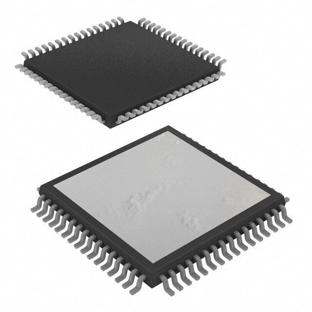
| 供应商器件封装 | 64-HTQFP(14x14) |
| 其它名称 | 296-25589 |
| 包装 | 托盘 |
| 商标 | Texas Instruments |
| 安装类型 | 表面贴装 |
| 安装风格 | SMD/SMT |
| 封装 | Tray |
| 封装/外壳 | 64-TQFP 裸露焊盘 |
| 封装/箱体 | HTQFP-64 |
| 工作温度 | 0°C ~ 70°C (TA) |
| 工厂包装数量 | 90 |
| 最大功率耗散 | 1.8 W |
| 最大工作温度 | + 150 C |
| 最小工作温度 | 0 C |
| 标准包装 | 90 |
| 特性 | 消除爆音,数字输入,短路和热保护,关机 |
| 电压-电源 | 18 V ~ 38 V |
| 电源电压-最大 | 36 V |
| 电源电压-最小 | 12 V |
| 电源电流 | 20 mA |
| 类型 | D 类 |
| 系列 | TAS5614 |
| 输入信号类型 | Differential, Single |
| 输出功率 | 150 W, 300 W |
| 输出类型 | 1-通道(单声道)或 2-通道(立体声) |


- 商务部:美国ITC正式对集成电路等产品启动337调查
- 曝三星4nm工艺存在良率问题 高通将骁龙8 Gen1或转产台积电
- 太阳诱电将投资9.5亿元在常州建新厂生产MLCC 预计2023年完工
- 英特尔发布欧洲新工厂建设计划 深化IDM 2.0 战略
- 台积电先进制程称霸业界 有大客户加持明年业绩稳了
- 达到5530亿美元!SIA预计今年全球半导体销售额将创下新高
- 英特尔拟将自动驾驶子公司Mobileye上市 估值或超500亿美元
- 三星加码芯片和SET,合并消费电子和移动部门,撤换高东真等 CEO
- 三星电子宣布重大人事变动 还合并消费电子和移动部门
- 海关总署:前11个月进口集成电路产品价值2.52万亿元 增长14.8%


PDF Datasheet 数据手册内容提取
TAS5614 www.ti.com SLAS680A–DECEMBER2009–REVISEDJANUARY2010 150W STEREO / 300W MONO PurePath™ HD DIGITAL-INPUT POWER STAGE CheckforSamples:TAS5614 FEATURES APPLICATIONS 1 • PurePath™HDEnabledIntegratedFeedback • HomeTheaterSystems 23 Provides: • AVReceivers – SignalBandwidthupto80kHzforHigh • DVD/Blu-ray™Receivers FrequencyContentFromHDSources • MiniComboSystems – Ultralow0.03%THDat1Winto4Ω • ActiveSpeakersandSubwoofers – Ultralow0.01%THDat1Winto8Ω DESCRIPTION – FlatTHDatallFrequenciesforNatural Sound The TAS5614 is a high performance analog input Class D amplifier with integrated closed loop – 80dBPSRR(BTL,NoInputSignal) feedback technology (known as PurePath™ HD) with – >100dB(Aweighted)SNR the ability to drive up to 150W (1) Stereo into 4 to 8 Ω – ClickandPopFreeStartup Speakersfromasingle36Vsupply. • PincompatiblewithTAS5631,TAS5616and PurePath™ HD technology enables traditional TAS5612 AB-Amplifier performance (<0.03% THD) levels while • MultipleConfigurationsPossibleontheSame providing the power efficiency of traditional class D PCBWithStuffingOptions: amplifiers. – MonoParallelBridgeTiedLoad(PBTL) Unlike traditional Class D amplifiers, the distortion – StereoBridgeTiedLoad(BTL) curve only increases once the output levels move into clipping.PurePath™HDPowerPAD™ – 2.1SingleEndedStereoPairandBridge TiedLoadSubwoofer PurePath™ HD technology enables lower idle losses makingthedeviceevenmoreefficient. • TotalOutputPowerat10%THD+N – 300WinMonoPBTLConfiguration TTOOTTAALLHHAARRMMOONNIICCDDIISSTTOORRTTIIOONN++NNOOIISSEE VVSS – 150WperChannelinStereoBTL OOUUTTPPUUTTPPOOWWEERR 1100 Configuration 44OOhhmm((66kkHHzz)) 44OOhhmm((11kkHHzz)) • TotalOutputPowerinBTLConfigurationat %% 1–%T16H0DW+NStereointo3Ω Distortion-Distortion- 11 – 125WStereointo4Ω monicmonic 00,,11 – 85WStereointo6Ω HarHar – 65WStereointo8Ω talTotal N- 0,01 • >90%EfficienctPowerStageWith60-mΩ D+ H T OutputMOSFETs TC=75C CONFIG=BTL • Self-ProtectionDesign(Including 0,001 0,01 1 100 Undervoltage,Overtemperature,Clipping,and PO-OutputPower-W Short-CircuitProtection)WithErrorReporting • EMICompliantWhenUsedWith RecommendedSystemDesign • TwoThermallyEnhancedPackageOptions: (1) Achievableoutputpowerlevelsaredependentonthethermal configurationofthetargetapplication.Ahighperformance – PHD(64-PinQFP) thermalinterfacematerialbetweenthepackageexposed heatslugandtheheatsinkshouldbeusedtoachievehigh – DKD(44-PinPSOP3) outputpowerlevels. 1 Pleasebeawarethatanimportantnoticeconcerningavailability,standardwarranty,anduseincriticalapplicationsofTexas Instrumentssemiconductorproductsanddisclaimerstheretoappearsattheendofthisdatasheet. PurePath,PowerPADaretrademarksofTexasInstruments. 2 Allothertrademarksarethepropertyoftheirrespectiveowners. 3 UNLESS OTHERWISE NOTED this document contains Copyright©2009–2010,TexasInstrumentsIncorporated PRODUCTION DATA information current as of publication date. Products conform to specifications per the terms of Texas Instruments standard warranty. Production processing does not necessarilyincludetestingofallparameters.
TAS5614 SLAS680A–DECEMBER2009–REVISEDJANUARY2010 www.ti.com Thesedeviceshavelimitedbuilt-inESDprotection.Theleadsshouldbeshortedtogetherorthedeviceplacedinconductivefoam duringstorageorhandlingtopreventelectrostaticdamagetotheMOSgates. DEVICE INFORMATION Terminal Assignment Both package types contains a heat slug that is located on the top side of the device for convenient thermal couplingtotheheatsink. PHD PACKAGE DKD PACKAGE (TOPVIEW) (TOPVIEW) VDDPSU_REFNCNCNCNCGNDGNDGVDD_BGVDD_ABST_AOUT_AOUT_APVDD_APVDD_AGND_A PSU_REF 1 44 GVDD_AB VDD 2 43 BST_A OC_ADJ 3 42 PVDD_A 4321098765432109 RESET 4 41 PVDD_A ORCE_SAEDTJ 2166666555555555544478 GGNNDD__AB C_STARTUP 5 40 OUT_A C_STARTUP 3 46 GND_B INPUT_A 6 39 OUT_A INPUT_A 4 45 OUT_B INPUT_B 7 38 GND_A INPUT_B 5 44 OUT_B VI_CM 8 37 GND_B VI_CM 6 43 PVDD_B GND 7 42 PVDD_B GND 9 44 36 OUT_B INPAVUGRTNE_CGD 1980 344901 PBBVSSDTT__DCC_C AVGRNEGD 1110 (TOPpinsP 3354 BPSVTD_DB_B INPUTTE_SDT 1112 3378 OPVUDTD_C_C IINNPPUUTT__DC 1132 VIEWACK 3332 BPSVTD_DC_C NC 13 36 OUT_C TEST 14 )AG 31 OUT_C NC 14 35 GND_C E SD 15 64-pins QFPpackage 34 GND__C NC 15 30 GND_C OTW1 161718192021222324252627282930313233 GND_D SNDC 1167 2298 GONUDT__DD OTW 18 27 OUT_D READY 19 26 PVDD_D OTW2CLIPREADYM1M2M3GNDGNDVDD_CVDD_DBST_DOUT_DOUT_DVDD_DVDD_DGND_D MM21 2201 2254 PBVSDT_DD_D GG PP M3 22 23 GVDD_CD PIN ONE LOCATION PHD PACKAGE Electrical Pin 1 Pin 1 Marker White Dot 2 SubmitDocumentationFeedback Copyright©2009–2010,TexasInstrumentsIncorporated ProductFolderLink(s):TAS5614
TAS5614 www.ti.com SLAS680A–DECEMBER2009–REVISEDJANUARY2010 MODE SELECTION PINS MODEPINS OUTPUT PWMINPUT(1) DESCRIPTION M3 M2 M1 CONFIGURATION 0 0 0 2N 2×BTL ADmode 0 0 1 — — Reserved 0 1 0 2N 2×BTL BDmode 0 1 1 1N 1×BTL+2×SE ADmode 1 0 0 1N 4×SE ADmode INPUT_C(2) INPUT_D(2) 2N 1 0 1 1×PBTL 0 0 ADmode 1N 1 0 BDmode 1 1 0 Reserved 1 1 1 (1) The1Nand2NnamingconventionisusedtoindicatethenumberofPWMlinestothepowerstageperchannelinaspecificmode. (2) INPUT_CandDareusedtoselectbetweenasubsetofADandBDmodeoperationsinPBTLmode PACKAGE HEAT DISSIPATION RATINGS(1) PARAMETER TAS5614PHD TAS5614DKD R (°C/W)–2BTLor4SEchannels 3.2 2.1 qJC R (°C/W)–1BTLor2SEchannel(s) 5.4 3.5 qJC R (°C/W)–1SEchannel 7.9 5.1 qJC PadArea (2) 64mm2 80mm2 (1) J isjunction-to-case,C iscase-to-heatsink C H (2) R isanimportantconsideration.Assumea2-milthicknessofthermalgreasewithathermalconductivityof2.5W/mKbetweenthe qCH padareaandtheheatsinkandbothchannelsactive.TheR withthisconditionis1.1°C/WforthePHDpackageand0.44°C/Wfor qCH theDKDpackage. Table1. ORDERINGINFORMATION(1) T PACKAGE DESCRIPTION A 0°C–70°C TAS5614PHD 64pinHTQFP 0°C–70°C TAS5614DKD 44pinPSOP3 (1) Forthemostcurrentpackageandorderinginformation,seethePackageOptionAddendumattheendofthisdocument,orseetheTI websiteatwww.ti.com. Copyright©2009–2010,TexasInstrumentsIncorporated SubmitDocumentationFeedback 3 ProductFolderLink(s):TAS5614
TAS5614 SLAS680A–DECEMBER2009–REVISEDJANUARY2010 www.ti.com ABSOLUTE MAXIMUM RATINGS overoperatingfree-airtemperaturerangeunlessotherwisenoted (1) TAS5614 UNIT VDDtoGND –0.3to13.2 V GVDDtoGND –0.3to13.2 V PVDD_XtoGND_X(2) –0.3to53 V OUT_XtoGND_X(2) –0.3to53 V BST_XtoGND_X(2) –0.3to66.2 V BST_XtoGVDD_X(2) –0.3to53 V VREGtoGND –0.3to4.2 V GND_XtoGND –0.3to0.3 V GNDtoAGND –0.3to0.3 V OC_ADJ,M1,M2,M3,OSC_IO+,OSC_IO-,FREQ_ADJ,VI_CM,C_STARTUP,PSU_REF –0.3to4.2 V toGND INPUT_X –0.3to7 V RESET,SD,OTW1,OTW2,CLIP,READYtoGND –0.3to7 V Maximumcontinuoussinkcurrent(SD,OTW1,OTW2,CLIP,READY) 9 mA Maximumoperatingjunctiontemperaturerange,T 0to150 °C J Storagetemperature,T –40to150 °C stg Humanbodymodel(3)(allpins) ±2 kV Electrostaticdischarge Chargeddevicemodel(3)(allpins) ±500 V (1) StressesbeyondthoselistedunderAbsoluteMaximumRatingsmaycausepermanentdamagetothedevice.Thesearestressratings only,andfunctionaloperationofthedeviceattheseoranyotherconditionsbeyondthoseindicatedunderRecommendedOperating Conditionsisnotimplied.Exposuretoabsolute-maximum-ratedconditionsforextendedperiodsmayaffectdevicereliability. (2) ThesevoltagesrepresentstheDCvoltage+peakACwaveformmeasuredattheterminalofthedeviceinallconditions. (3) Failuretofollowgoodanti-staticESDhandlingduringmanufactureandreworkwillcontributetodevicemalfunction.Makesurethe operatorshandlingthedeviceareadequatelygroundedthroughtheuseofgroundstrapsoralternativeESDprotection. RECOMMENDED OPERATING CONDITIONS overoperatingfree-airtemperaturerange(unlessotherwisenoted) MIN NOM MAX UNIT PVDD_x Half-bridgesupply DCsupplyvoltage 18 36 38 V Supplyforlogicregulatorsandgate-drive GVDD_x DCsupplyvoltage 10.8 12 13.2 V circuitry VDD Digitalregulatorsupplyvoltage DCsupplyvoltage 10.8 12 13.2 V R (BTL) 3.5 4 L Outputfitleraccordingtoschematicsin R (SE) Loadimpedance 2.8 3 Ω L theapplicationinformationsection. R (PBTL) 1.6 2 L Outputfitleraccordingtoschematicsin theapplicationinformationsection.R = R (BTL) Loadimpedance OC 2.8 3 Ω L 22kΩ,addSchottkydiodesfromOUT_X toGND_X. L (BTL) 7 10 OUTPUT L (SE) Outputfilterinductance MinimumoutputinductanceatI 7 15 mH OUTPUT OC L (PBTL) 7 10 OUTPUT F PWMframerate 352 384 500 kHz PWM C PVDDclosedecouplingcapacitors 2.0 mF PVDD R Over-currentprogrammingresistor Resistortolerance=5% 22 30 kΩ OC R Over-currentprogrammingresistor Resistortolerance=5% 47 64 kΩ OC_LATCHED T Junctiontemperature 0 150 °C J 4 SubmitDocumentationFeedback Copyright©2009–2010,TexasInstrumentsIncorporated ProductFolderLink(s):TAS5614
TAS5614 www.ti.com SLAS680A–DECEMBER2009–REVISEDJANUARY2010 PINFUNCTIONS PIN FUNCTION(1) DESCRIPTION NAME PHDNO. DKDNO. AGND 8 10 P Analogground BST_A 54 43 P HSbootstrapsupply(BST),external0.033mFcapacitortoOUT_Arequired. BST_B 41 34 P HSbootstrapsupply(BST),external0.033mFcapacitortoOUT_Brequired. BST_C 40 33 P HSbootstrapsupply(BST),external0.033mFcapacitortoOUT_Crequired. BST_D 27 24 P HSbootstrapsupply(BST),external0.033mFcapacitortoOUT_Drequired. CLIP 18 — O Clippingwarning;opendrain;activelow C_STARTUP 3 5 O Startupramprequiresachargingcapacitorof4.7nFtoGND TEST 12 14 I ConnecttoVREGnode GND 7,23,24,57,58 9 P Ground GND_A 48,49 38 P Powergroundforhalf-bridgeA GND_B 46,47 37 P Powergroundforhalf-bridgeB GND_C 34,35 30 P Powergroundforhalf-bridgeC GND_D 32,33 29 P Powergroundforhalf-bridgeD GVDD_A 55 — P Gatedrivevoltagesupplyrequires0.1mFcapacitortoGND GVDD_B 56 — P Gatedrivevoltagesupplyrequires0.1mFcapacitortoGND GVDD_C 25 — P Gatedrivevoltagesupplyrequires0.1mFcapacitortoGND GVDD_D 26 — P Gatedrivevoltagesupplyrequires0.1mFcapacitortoGND GVDD_AB — 44 P Gatedrivevoltagesupplyrequires0.22mFcapacitortoGND GVDD_CD — 23 P Gatedrivevoltagesupplyrequires0.22mFcapacitortoGND INPUT_A 4 6 I InputsignalforhalfbridgeA INPUT_B 5 7 I InputsignalforhalfbridgeB INPUT_C 10 12 I InputsignalforhalfbridgeC INPUT_D 11 13 I InputsignalforhalfbridgeD M1 20 20 I Modeselection M2 21 21 I Modeselection M3 22 22 I Modeselection NC 59–62 – — Noconnect,pinsmaybegrounded. NC 13,14 15,16 — Noconnect,pinsmaybegrounded. OC_ADJ 1 3 O Analogovercurrentprogrammingpinrequiresresistortoground. OTW — 18 O Overtemperaturewarningsignal,opendrain,activelow. OTW1 16 — O Overtemperaturewarningsignal,opendrain,activelow. OTW2 17 — O Overtemperaturewarningsignal,opendrain,activelow. OUT_A 52,53 39,40 O Output,halfbridgeA OUT_B 44,45 36 O Output,halfbridgeB OUT_C 36,37 31 O Output,halfbridgeC OUT_D 28,29 27,28 O Output,halfbridgeD PSU_REF 63 1 P PSUReferencerequiresclosedecouplingof4.7mFtoGND PowersupplyinputforhalfbridgesArequiresclosedecouplingof2mFcapacitorto PVDD_A 50,51 41,42 P GND_A PowersupplyinputforhalfbridgesBrequiresclosedecouplingof2mFcapacitorto PVDD_B 42,43 35 P GND_B PowersupplyinputforhalfbridgesCrequiresclosedecouplingof2mFcapacitorto PVDD_C 38,39 32 P GND_C PowersupplyinputforhalfbridgesDrequiresclosedecouplingof2mFcapacitorto PVDD_D 30,31 25,26 P GND_D READY 19 19 O Normaloperation;opendrain;activehigh RESET 2 4 I DeviceresetInput;activelow SD 15 17 O Shutdownsignal,opendrain,activelow Powersupplyfordigitalvoltageregulatorrequiresa47mFcapacitorinparallelwitha VDD 64 2 P 0.1mFcapacitortoGNDfordecoupling. VI_CM 6 8 O Analogcomparatorreferencenoderequiresclosedecouplingof4.7mFtoGND (1) I=Input,O=Output,P=Power Copyright©2009–2010,TexasInstrumentsIncorporated SubmitDocumentationFeedback 5 ProductFolderLink(s):TAS5614
TAS5614 SLAS680A–DECEMBER2009–REVISEDJANUARY2010 www.ti.com PINFUNCTIONS(continued) PIN FUNCTION(1) DESCRIPTION NAME PHDNO. DKDNO. VREG 9 11 P Digitalregulatorsupplyfilterpinrequires0.1mFcapacitortoGND TYPICAL SYSTEM BLOCK DIAGRAM Capsfor System External microcontroller Filtering and AMPRESET (2) Startup/Stop I2C TTTAAASSS555550108886// VALID *NOTE1 RESET /SD OTW2,/OTW /CLIP READY VI_CM PSU_REF C_STARTUP BST_A OTW1,/ BST_B BoCoatsptsrap / PWM_A INPUT_A OUT_A 2ndOrder ChLaenftn-el PWM_B INPUT_B H-BInripdugte1 H-OBuritdpguet1 OUT2_B L-FCiltOeruftoprut Output each 2 H-Bridge 2-CHANNEL H-BRIDGE BTLMODE PWM_C INPUT_C OUT_C 2ndOrder Right- Input Output L-COutput Channel PWM_D INPUT_D H-Bridge2 H-Bridge2 OUT2_D Filterfor Output each 2 H-Bridge HCaMorodndwtreoirle MMM213 PVDD_A,B,C,D GND_A,B,C,D GVDD_A,B,C,D GND VDD VREG AGND TEST OC_ADJ BBSSTT__CD BoCoatsptsrap 8 8 4 PVDD PVDD GVDD,VDD, Hardwire 3560VV PowerSupply andVREG Over- SYSTEM Decoupling PowerSupply Current Power Decoupling Limit Supplies GND GND GVDD(12V)/VDD(12V) 12V VAC (1) LogicANDisinsideoroutsidethemicrocontroller. 6 SubmitDocumentationFeedback Copyright©2009–2010,TexasInstrumentsIncorporated ProductFolderLink(s):TAS5614
TAS5614 www.ti.com SLAS680A–DECEMBER2009–REVISEDJANUARY2010 FUNCTIONAL BLOCK DIAGRAM CLIP READY OTW1 OTW2 SD MM12 LOGIC VDD M3 &I/O RESET PROTECTION PORTWEEESMREP-TUP GVDD_A UVP GVDD_C VREG AVRGENGD C_STARTUP CSOTANRTTRUOPL SENSE GVDD_B GVDD_D GND PORVOETRE-CLOTIAODN CB3C CUSERNRSEENT OC_ADJ PPSC 444 POGVUNDTDD__X_XX GVDD_A PWM ACTIVITY BST_A DETECTOR PVDD_A REPCWEIMVER CONTROL CTOINMTINRGOL GATE-DRIVE OUT_A GND_A PSU_REF GVDD_B VI_CM ANALOG - BST_B INPUT_A LOOPFILTER + PVDD_B ANALOG + REPCWEIMVER CONTROL CTOINMTINRGOL GATE-DRIVE OUT_B INPUT_B LOOPFILTER - INPUT_C AGC 4 GPVNDDD_X LOAONPAFLIOLTGER ANALOGINPUTMUX +- ANALOGCOMPARATORMUX REPCWEIMVER CONTROL CTOINMTINRGOL GATE-DRIVE GGOPBVSNVUDTDDT_D_D_CCB__CC INPUT_D ANALOG + GND_C LOOPFILTER - GVDD_D BST_D PVDD_D REPCWEIMVER CONTROL CTOINMTINRGOL GATE-DRIVE OUT_D GND_D Copyright©2009–2010,TexasInstrumentsIncorporated SubmitDocumentationFeedback 7 ProductFolderLink(s):TAS5614
TAS5614 SLAS680A–DECEMBER2009–REVISEDJANUARY2010 www.ti.com AUDIO CHARACTERISTICS (BTL) AudioperformanceisrecordedasachipsetconsistingofaTAS5518PWMProcessor(modulationindexlimitedto97.7%) andaTAS5614powerstage.PCBandsystemconfigurationsareinaccordancewithrecommendedguidelines.Audio frequency=1kHz,PVDD_X=36V,GVDD_X=12V,R =4Ω,f =384kHz,R =30kΩ,T =75°C, L S OC C OutputFilter:L =7mH,C =680nF,MODE=000,unlessotherwisenoted. DEM DEM PARAMETER TESTCONDITIONS MIN TYP MAX UNIT R =3Ω,10%THD+N(R =22kΩ,addSchottky L OC 200 diodesfromOUT_XtoGND_X.) R =4Ω,10%THD+N 150 L P Poweroutputperchannel W O R =3Ω,1%THD+N(R =22kΩ,addSchottky L OC 160 diodesfromOUT_XtoGND_X.) R =4Ω,1%THD+N 125 L 1W,R =4Ω 0.03% L THD+N Totalharmonicdistortion+noise 1W,R =8Ω 0.01% L V Outputintegratednoise A-weighted,TAS5518Modulator 125 mV n |V | Outputoffsetvoltage Nosignal 20 40 mV OS SNR Signal-to-noiseratio(1) A-weighted,TAS5518Modulator 103 dB A-weighted,inputlevel–60dBFSusingTAS5518 DNR Dynamicrange 103 dB modulator P PowerdissipationduetoIdlelosses P =0,4channelsswitching(2) 2.6 W idle (I ) O PVDD_X (1) SNRiscalculatedrelativeto1%THD-Noutputlevel. (2) Actualsystemidlelossesalsoareaffectedbycorelossesofoutputinductors. 8 SubmitDocumentationFeedback Copyright©2009–2010,TexasInstrumentsIncorporated ProductFolderLink(s):TAS5614
TAS5614 www.ti.com SLAS680A–DECEMBER2009–REVISEDJANUARY2010 AUDIO CHARACTERISTICS (PBTL) AudioperformanceisrecordedasachipsetconsistingofaTAS5518PWMProcessor(modulationindexlimitedto97.7%) andaTAS5614powerstage.PCBandsystemconfigurationsareinaccordancewithrecommendedguidelines.Audio frequency=1kHz,PVDD_X=36V,GVDD_X=12V,R =2Ω,f =384kHz,R =30kΩ,T =75°C, L S OC C OutputFilter:L =7mH,C =1mF,MODE=101-00,unlessotherwisenoted. DEM DEM PARAMETER TESTCONDITIONS MIN TYP MAX UNIT R =2Ω,10%,THD+N 300 L R =3Ω,10%,THD+N 200 L R =4Ω,10%,THD+N 160 L P Poweroutputperchannel W O R =2Ω,1%THD+N 250 L R =3Ω,1%THD+N 160 L R =4Ω,1%THD+N 130 L THD+N Totalharmonicdistortion+noise 1W 0.03% V Outputintegratednoise A-weighted,TAS5518Modulator 128 mV n SNR Signaltonoiseratio(1) A-weighted,TAS5518Modulator 103 dB A-weighted,inputlevel–60dBFSusing DNR Dynamicrange 103 dB TAS5518modulator P Powerdissipationduetoidlelosses(I ) P =0,4channelsswitching(2) 2.4 W idle PVDD_X O (1) SNRiscalculatedrelativeto1%THD-Noutputlevel. (2) Actualsystemidlelossesareaffectedbycorelossesofoutputinductors. ELECTRICAL CHARACTERISTICS PVDD_X=36V,GVDD_X=12V,VDD=12V,T (Casetemperature)=75°C,f =384kHz,unlessotherwisespecified. C S PARAMETER TESTCONDITIONS MIN TYP MAX UNIT INTERNALVOLTAGEREGULATORANDCURRENTCONSUMPTION Voltageregulator,onlyusedasreference VREG VDD=12V 3 3.3 3.6 V node,VREG VI_CM Analogcomparatorreferencenode,VI_CM 1.5 1.75 1.9 V Operating,50%dutycycle 20 I VDDsupplycurrent mA VDD Idle,resetmode 20 50%dutycycle 10 I Gate-supplycurrentperhalf-bridge mA GVDD_x Resetmode 1.5 50%dutycyclewithoutoutputfilteror 16.8 mA I Half-bridgeidlecurrent load PVDD_x Resetmode,Noswitching 620 mA OUTPUT-STAGEMOSFETs Drain-to-sourceresistance,lowside(LS) T =25°C,excludesmetallization 60 100 mΩ J R resistance, DS(on) Drain-to-sourceresistance,highside(HS) GVDD=12V 60 100 mΩ Copyright©2009–2010,TexasInstrumentsIncorporated SubmitDocumentationFeedback 9 ProductFolderLink(s):TAS5614
TAS5614 SLAS680A–DECEMBER2009–REVISEDJANUARY2010 www.ti.com ELECTRICAL CHARACTERISTICS (continued) PVDD_X=36V,GVDD_X=12V,VDD=12V,T (Casetemperature)=75°C,f =384kHz,unlessotherwisespecified. C S PARAMETER TESTCONDITIONS MIN TYP MAX UNIT I/OPROTECTION V Undervoltageprotectionlimit,GVDD_x 10 V uvp,G V (1) 0.6 V uvp,hyst OTW1(1) Overtemperaturewarning1 95 100 105 °C OTW2(1) Overtemperaturewarning2 115 125 135 °C TemperaturedropneededbelowOTW OTW (1) temperatureforOTWtobeinactiveafter 25 °C hyst OTWevent. Overtemperatureerror 145 155 165 °C OTE(1) OTE-OTWdifferential 30 °C OTE (1) AresetneedstooccurforSDtobereleased 25 °C HYST followinganOTEevent OLPC Overloadprotectioncounter f =384kHz 2.6 ms PWM Resistor–programmable,nominalpeak 14 currentin1Ωload,R =30kΩ OCP I Overcurrentlimitprotection Resistor–programmable,nominalpeak A OC currentin1Ωload,R =22kΩ OCP 18 (WithSchottkydiodesfromOUT_Xto GND_X.) Resistor–programmable,nominalpeak 14 currentin1Ωload,R =64kΩ OCP I Overcurrentlimitprotection Resistor–programmable,nominalpeak A OC_LATCHED currentin1Ωload,R =47kΩ OCP 18 (WithSchottkydiodesfromOUT_Xto GND_X.) Timefromapplicationofshortconditionto I Overcurrentresponsetime 150 ns OCT Hi-Zofaffectedhalfbridge ConnectedwhenRESETisactiveto Internalpulldownresistoratoutputofeach I providebootstrapcharge.NotusedinSE 3 mA PD halfbridge mode. STATICDIGITALSPECIFICATIONS V Highlevelinputvoltage 1.9 V IH INPUT_X,M1,M2,M3,RESET V Lowlevelinputvoltage 0.8 V IL I Inputleakagecurrent 100 mA lkg OTW/SHUTDOWN(SD) Internalpullupresistance,OTW1toVREG, R 20 26 33 kΩ INT_PU OTW2toVREG,SDtoVREG Internalpullupresistor 3 3.3 3.6 V Highleveloutputvoltage V OH Externalpullupof4.7kΩto5V 4.5 5 V Lowleveloutputvoltage I =4mA 200 500 mV OL O DevicefanoutOTW1,OTW2,SD,CLIP, FANOUT Noexternalpullup 30 devices READY (1) Specifiedbydesign. 10 SubmitDocumentationFeedback Copyright©2009–2010,TexasInstrumentsIncorporated ProductFolderLink(s):TAS5614
TAS5614 www.ti.com SLAS680A–DECEMBER2009–REVISEDJANUARY2010 TYPICAL CHARACTERISTICS, BTL CONFIGURATION TOTALHARMONIC+NOISE OUTPUTPOWER vs vs OUTPUTPOWER SUPPLYVOLTAGE 10 250 % TC= 75°C 3W TC= 75°C se - 4W THD+N 10% oi 200 3W N 6W on + 1 8W W 4W storti wer - 150 6W Di Po 8W monic 0.1 utput 100 r O Ha - al PO ot 0.01 T N - 50 + D H T 0.001 0 0.01 0.1 1 10 100 1000 18192021222324252627282930313233343536 PV - Supply Voltage - V P - Output Power - W DD O Figure1. Figure2. UNCLIPPEDOUTPUTPOWER SYSTEMEFFICIENCY vs vs SUPPLYVOLTAGE OUTPUTPOWER 200 100 T = 75°C C 90 80 8W 6W 4W 3W 150 W 4W 70 ower - 8W 6W y - % 60 put P 100 cienc 50 Out Effi 40 - O 30 P 50 20 T = 25°C C 10 THD+N = 10% 0 0 18192021222324252627282930313233343536 0 50 100 150 200 250 300 350 400 PV - Supply Voltage - V 2 Channel Output Power - W DD Figure3. Figure4. Copyright©2009–2010,TexasInstrumentsIncorporated SubmitDocumentationFeedback 11 ProductFolderLink(s):TAS5614
TAS5614 SLAS680A–DECEMBER2009–REVISEDJANUARY2010 www.ti.com TYPICAL CHARACTERISTICS, BTL CONFIGURATION (continued) SYSTEMSPOWERLOSS OUTPUTPOWER vs vs OUTPUTPOWER CASETEMPERATURE 30 250 T = 25°C THD+N = 10% C 3W THD+N = 10% 4W 200 4W W 20 W r - ss - 6W owe 150 6W o P wr L put o ut 100 P O 10 - PO 8W 8W 50 0 0 0 50 100 150 200 250 300 350 400 20 30 40 50 60 70 80 90 100 2 Channel Output Power - W T - Case Temperature - °C C Figure5. Figure6. NOISEAMPLITUDE TOTALHORMONICDISTORTION+NOISE vs vs FREQUENCY FREQUENCY 0 10 T = 75°C, R = 4W, C L -20 REF = 25.46 V, % TC= 75°C, SFFaTm Splieze R =a t1e6 =3 8448 kHz, n - Toroidal Output Inductors o -40 rti 1 dB sto ude - -60 nic Di plit -80 mo 0.1 m ar A H Noise --112000 N - Total 0.01 1W 4W D+ H -140 T 21 W (1/8 Power) -160 0.001 0 5 10 15 20 10 100 1k 10k 100k f - Frequency - kHz f - Frequency - Hz Figure7. Figure8. 12 SubmitDocumentationFeedback Copyright©2009–2010,TexasInstrumentsIncorporated ProductFolderLink(s):TAS5614
TAS5614 www.ti.com SLAS680A–DECEMBER2009–REVISEDJANUARY2010 TYPICAL CHARACTERISTICS, PBTL CONFIGURATION TOTALHARMONIC+NOISE OUTPUTPOWER vs vs OUTPUTPOWER SUPPLYVOLTAGE 10 400 % TC= 75°C 2W TC= 75°C e - 3W 350 THD+N = 10% s 2W oi N 4W + 1 300 3W n 6W W ortio 8W er - 250 4W Dist Pow 6W nic 0.1 put 200 8W mo ut r O 150 al Ha P- O ot 0.01 100 T N - + 50 D H T 0.001 0 0.01 0.1 1 10 100 1000 18192021222324252627282930313233343536 PO- Output Power - W PVDD- Supply Voltage - V Figure9. Figure10. OUTPUTPOWER vs CASETEMPERATURE 400 THD+N = 10% 2W 350 300 3W W r - 250 e w o 4W P ut 200 p ut 6W O 150 - O P 100 8W 50 0 20 30 40 50 60 70 80 90 100 T - Case Temperature - °C C Figure11. Copyright©2009–2010,TexasInstrumentsIncorporated SubmitDocumentationFeedback 13 ProductFolderLink(s):TAS5614
TAS5614 SLAS680A–DECEMBER2009–REVISEDJANUARY2010 www.ti.com APPLICATION INFORMATION PCB MATERIAL RECOMMENDATION FR-4 Glass Epoxy material with 2oz. (70mm) is recommended for use with the TAS5614. The use of this material can provide for higher power output, improved thermal performance, and better EMI margin (due to lower PCB traceinductance. PVDD CAPACITOR RECOMMENDATION The large capacitors used in conjunction with each full-bridge, are referred to as the PVDD Capacitors. These capacitors should be selected for proper voltage margin and adequate capacitance to support the power requirements. In practice, with a well designed system power supply, 1000mF, 50V support more applications. The PVDD capacitors should be low ESR type because they are used in a circuit associated with high-speed switching. DECOUPLING CAPACITOR RECOMMENDATION To design an amplifier that has robust performance, passes regulatory requirements, and exhibits good audio performance, good quality decoupling capacitors should be used. In practice, X7R should be used in this application. The voltage of the decoupling capacitors should be selected in accordance with good design practices. Temperature, ripple current, and voltage overshoot must be considered. This fact is particularly true in the selection of the 0.1mF that is placed on the power supply to each half-bridge. It must withstand the voltage overshoot of the PWM switching, the heat generated by the amplifier during high power output, and the ripple current created by high power output. A minimum voltage rating of 50V is required for use with a 36V power supply. SYSTEM DESIGN RECOMMENDATIONS ThefollowingschematicsandPCBlayoutsillustratebestpracticesintheuseoftheTAS5614. 14 SubmitDocumentationFeedback Copyright©2009–2010,TexasInstrumentsIncorporated ProductFolderLink(s):TAS5614
TAS5614 www.ti.com SLAS680A–DECEMBER2009–REVISEDJANUARY2010 GVDD/VDD (+12V) PVDD OUT_LEFT_P + - OUT_LEFT_M PVDDR74R743.3R3.3R GNDC78C7810nF10nF GND GNDOUT_RIGHT_P + - OUT_RIGHT_R PVDD GVDD/VDD (+12V) CC646410001000uFuF GND C69C692.2uF2.2uF GND GND C67C671000uF1000uF GND RR70703.33.3RR C74C7410nF10nF C75C7510nF10nF R71R713.3R3.3R C68C6847uF47uF63V63V GND R72R723.3R3.3R C76C7610nF10nF C77C7710nF10nF R73R733.3R3.3R GND CCCC5050707068681n1n0nF0nFFF GND C71C71C51C511nF1nF680nF680nF 1000uF1000uFC66C66 GNDGND C52C52C72C72680n680n1nF1nFFF GND C53C53C73C73680nF680nF1nF1nF 1000uF1000uFC65C65 L10L107uH7uH L11L117uH7uH C41C4133nF33nF C42C4233nF33nF 7uH7uHL12L12 L13L137uH7uH GND C61C612uF C62C622uF GND GND GND_A GND_B GND_B OUT_B OUT_B PVDD_B PVDD_B BST_B BST_C PVDD_C PVDD_C OUT_C OUT_C GND_C GND_C GND_D CC60602uF A_DNG D_DNG C63C632uF A_DDVP D_DDVP A_DDVP D_DDVP A_TUO D_TUO RR3131CC40403333nFnF3.3R3.3R CCCC30303131100n100n100n100nFFFF GND ABAACCCCDD____NNNNNNDDTTGGUSDDBOVVGG U10U10TAS5614PHD CDY__DDDDD__DDDDTATNNUVVE123SMMMGGGGORB GND VREG C43C4333nF33nF R32R32GND3.3R3.3RR33R33 3.3R3.3R C32C32C33C33100nF100nF100nF100nF GNDGND RR3030 33.3R.3R FDEDRV_USP 2WPITLOC// C25C25C26C2610uF10uF100nF100nF GGNDND OC_ADJ /RESET C_STARTUP INPUT_A INPUT_B VI_CM GND AGND VREG INPUT_C INPUT_D TEST NC NC /SD /OTW1 C23C23 4.74.7uFuF R20R20 30kC20C20 4.7nF4.7nF C21C21 4.7uF4.7uF VREGGND VREG C22C22 100nF100nF GND GND GND GND VREG R19R1947k47k GND R18R18 C18C18100R100R100pF100pF GNDR10R10 100R100R R11R11 100R100R R12R12 100R100R R13R13 100R100R /SD /OTW1 /OTW2 /CLIP READY /RESET IN_LEFT_P IN_LEFT_N IN_RIGHT_P R_RIGHT_N Figure12. TypicalDifferential(2N)BTLApplicationWithBDModulationFilters Copyright©2009–2010,TexasInstrumentsIncorporated SubmitDocumentationFeedback 15 ProductFolderLink(s):TAS5614
TAS5614 SLAS680A–DECEMBER2009–REVISEDJANUARY2010 www.ti.com GVDD (+12V) PVDD 3.3R3.3R2.2uF2.2uF 10nF10nF GNDGND OUT_LEFT_P 3.3R3.3R 10nF10nF + -GND10nF10nF 3.3R3.3R OUT_LEFT_M PVDD GVDD (+12V) 47uF47uF1000uF1000uF GNDGND 1000uF1000uF GND 1uF1uF 1nF1nF GND1nF1nF 1uF1uF 1000uF1000uF GND 1000uF1000uF GND 7uH7uH 7uH7uH 7uH7uH 7uH7uH 33nF33nF 33nF33nF GND 2uF 2uF GND 48 47 46 45 44 43 42 41 40 39 38 37 36 35 34 33 2uF GND GND_A GND_B GND_B OUT_B OUT_B PVDD_B PVDD_B BST_B BST_C PVDD_C PVDD_C OUT_C OUT_C GND_C GND_C GND_D 2uF 94 A_DNG D_DNG 23 05 A_DDVP D_DDVP 13 15 A_DDVP D_DDVP 03 3.3R3.3R 3.3R3.3R 100nF100nF100nF100nF33nF33nF GNDGND GND 23456789015555555566 ACCCAADDBA_____NNNNNTTTDDGGSUUDDBOOVVGG TAS5614PHD CD__DDDDD___DDDDTTTNNUUVV123SMMMGGGGOOB 01234568972222222222 GNDGND VREG 33nF33nF3.3R3.3R 3.3R3.3R 100nF100nF100nF100nF GNDGND 26 CN YDAER 91 36 FER_USP PILC/ 81 10uF10uF100nF100nF GNDGND 4.7uF4.7uF 46 DDV 1OC_ADJ2/RESET3C_STARTUP4INPUT_A5INPUT_B6VI_CM7GND8AGND9VREG10INPUT_C11INPUT_D12TEST13NC14NC15/SD16/OTW1 2WTO/ 71 GND GND VREG VREG 30k 4.7nF4.7nF 4.7uF4.7uF 100nF100nF GND GND GND GND VREG 47k47k VREG GND 100pF100pF GND 100R100R 100R100R 100R100R VDD (+12V) /RESET IN_P IN_N /SD /OTW1 /OTW2 /CLIP READY Figure13. Typical(2N)PBTLApplicationWithBDModulationFilters 16 SubmitDocumentationFeedback Copyright©2009–2010,TexasInstrumentsIncorporated ProductFolderLink(s):TAS5614
TAS5614 www.ti.com SLAS680A–DECEMBER2009–REVISEDJANUARY2010 GVDD (+12V) PVDD PVDD PVDD GVDD (+12V) 10001000uFuF GNDOUT_LEFT_P 3.33.3RR 1nF1nF10n10nFF + -GND10nF10nF1nF1nF 3.3R3.3R OUT_LEFT_M 3.3R3.3R47uF47uF2.2uF2.2uF 10nF10nF GNDGNDGND OUT_RIGHT_P 3.3R3.3R 10nF10nF1nF1nF + -GND10nF10nF1nF1nF 3.3R3.3R OUT_RIGHT_M 1000uF1000uF GND 77uHuH 680n680nFF GND 680nF680nF 7uH7uH 1000uF1000uF1000uF1000uF GNDGND 7uH7uH 680nF680nF GND 680nF680nF 7uH7uH GND 2uF 2uF 2uF 2uF 1.5R1.5R 100nF100nF100nF100nF GND 33nF33nF GND 33nF33nF 33nF33nF GND 33nF33nF 1.5R1.5R 100nF100nF GND 44 43 42 41 40 39 38 37 36 35 34 33 32 31 30 29 28 27 26 25 24 23 100nF100nF GVDD_AB BST_A PVDD_A PVDD_A OUT_A OUT_A GND_A GND_B OUT_B PVDD_B BST_B BST_C PVDD_C OUT_C GND_C GND_D OUT_D OUT_D PVDD_D PVDD_D BST_D GVDD_CD PSU_REF VDD OC_ADJ /RESET C_STARTUP INPUT_A INPUT_B VI_CM GND AGND VREGTAS5614DKDINPUT_C INPUT_D TEST NC NC /SD /OTW READY M1 M2 M3 1 2 3 4 5 6 7 8 9 10 11 12 13 14 15 16 17 18 19 20 21 22 1100nF00nF GND GND VREG VREG GND 110uF0uF GND VREG 4.7uF4.7uF 30k 4.7nF4.7nF 4.7uF4.7uF 100nF100nF GND GND GND GND GND VREG 47k47k 100pF100pF GND 1100R00R 100R100R 100R100R 100R100R 100R100R VDD (+12V) /RESET IN_LEFT_P IN_LEFT_N IN_RIGHT_P IN_RIGHT_N /SD /OTW READY Figure14. TypicalDifferentialInputBTLApplicationwithBDModulationFiltersDKDPackage Copyright©2009–2010,TexasInstrumentsIncorporated SubmitDocumentationFeedback 17 ProductFolderLink(s):TAS5614
TAS5614 SLAS680A–DECEMBER2009–REVISEDJANUARY2010 www.ti.com THEORY OF OPERATION POWER SUPPLIES To facilitate system design, the TAS5614 needs only a 12V supply in addition to the (typical) 36V power-stage supply. An internal voltage regulator provides suitable voltage levels for the digital and low-voltage analog circuitry. Additionally, all circuitry requiring a floating voltage supply, e.g., the high-side gate drive, is accommodatedbybuilt-inbootstrapcircuitryrequiringonlyanexternalcapacitorforeachhalf-bridge. To provide outstanding electrical and acoustical characteristics, the PWM signal path including gate drive and output stage is designed as identical, independent half-bridges. For this reason, each half-bridge has separate gate drive supply (GVDD_X), bootstrap pins (BST_X), and power-stage supply pins (PVDD_X). Furthermore, an additionalpin(VDD)isprovidedassupplyforallcommoncircuits.Althoughsuppliedfromthesame12Vsource, it is highly recommended to separate GVDD_A, GVDD_B, GVDD_C, GVDD_D, and VDD on the printed-circuit board (PCB) by RC filters (see application diagram for details). These RC filters provide the recommended high-frequency isolation. Special attention should be paid to placing all decoupling capacitors as close to their associated pins as possible. In general, inductance between the power supply pins and decoupling capacitors mustbeavoided.(Seereferenceboarddocumentationforadditionalinformation.) Foraproperlyfunctioningbootstrapcircuit,asmallceramiccapacitormustbeconnectedfromeachbootstrappin (BST_X) to the power-stage output pin (OUT_X). When the power-stage output is low, the bootstrap capacitor is charged through an internal diode connected between the gate-drive power-supply pin (GVDD_X) and the bootstrap pin. When the power-stage output is high, the bootstrap capacitor potential is shifted above the output potential and thus provides a suitable voltage supply for the high-side gate driver. In an application with PWM switching frequencies in the range from 300kHz to 4000kHz, it is recommended to use 33nF ceramic capacitors, size 0603 or 0805, for the bootstrap supply. These 33-nF capacitors ensure sufficient energy storage, even during minimal PWM duty cycles, to keep the high-side power stage FET (LDMOS) fully turned on during the remainingpartofthePWMcycle. Special attention should be paid to the power-stage power supply; this includes component selection, PCB placement, and routing. As indicated, each half-bridge has independent power-stage supply pins (PVDD_X). For optimal electrical performance, EMI compliance, and system reliability, it is important that each PVDD_X pin is decoupled with a 2mF ceramic capacitor placed as close as possible to each supply pin. It is recommended to follow the PCB layout of the TAS5614 reference design. For additional information on recommended power supplyandrequiredcomponents,seetheapplicationdiagramsinthisdatasheet. The 12V supply should be from a low-noise, low-output-impedance voltage regulator. Likewise, the 36V power-stage supply is assumed to have low output impedance and low noise. The power-supply sequence is not critical as facilitated by the internal power-on-reset circuit. Moreover, the TAS5614 is fully protected against erroneous power-stage turn on due to parasitic gate charging. Thus, voltage-supply ramp rates (dV/dt) are non-criticalwithinthespecifiedrange(seetheRecommendedOperatingConditionstableofthisdatasheet). SYSTEM POWER-UP/POWER-DOWN SEQUENCE PoweringUp The TAS5614 does not require a power-up sequence. The outputs of the H-bridges remain in a high-impedance state until the gate-drive supply voltage (GVDD_X) and VDD voltage are above the undervoltage protection (UVP) voltage threshold (see the Electrical Characteristics table of this data sheet). Although not specifically required, it is recommended to hold RESET in a low state while powering up the device. This allows an internal circuittochargetheexternalbootstrapcapacitorsbyenablingaweakpulldownofthehalf-bridgeoutput. PoweringDown The TAS5614 does not require a power-down sequence. The device remains fully operational as long as the gate-drive supply (GVDD_X) voltage and VDD voltage are above the undervoltage protection (UVP) voltage threshold (see the Electrical Characteristics table of this data sheet). Although not specifically required, it is a goodpracticetoholdRESETlowduringpowerdown,thuspreventingaudibleartifactsincludingpopsorclicks. 18 SubmitDocumentationFeedback Copyright©2009–2010,TexasInstrumentsIncorporated ProductFolderLink(s):TAS5614
TAS5614 www.ti.com SLAS680A–DECEMBER2009–REVISEDJANUARY2010 ERROR REPORTING The SD, OTW, OTW1 and OTW2 pins are active-low, open-drain outputs. Their function is for protection-mode signalingtoaPWMcontrollerorothersystem-controldevice. Any fault resulting in device shutdown is signaled by the SD pin going low. Likewise, OTW and OTW2 goes low when the device junction temperature exceeds 125°C and OTW1 goes low when the junction temperature exceeds100°C(seethefollowingtable). OTW2, SD OTW1 DESCRIPTION OTW 0 0 0 Overtemperature(OTE)oroverload(OLP)orundervoltage(UVP) Overload(OLP)orundervoltage(UVP).Junctiontemperaturehigherthan100°C(overtemperature 0 0 1 warning) 0 1 1 Overload(OLP)orundervoltage(UVP) 1 0 0 Junctiontemperaturehigherthan125°C(overtemperaturewarning) 1 0 1 Junctiontemperaturehigherthan100°C(overtemperaturewarning) 1 1 1 Junctiontemperaturelowerthan100°CandnoOLPorUVPfaults(normaloperation) Note that asserting RESET low forces the SD signal high, independent of faults being present. TI recommends monitoring the OTW signal using the system micro controller and responding to an overtemperature warning signal by, e.g., turning down the volume to prevent further heating of the device resulting in device shutdown (OTE). To reduce external component count, an internal pullup resistor to 3.3V is provided on both SD and OTW outputs. Level compliance for 5V logic can be obtained by adding external pullup resistors to 5V (see the ElectricalCharacteristicstableofthisdatasheetforfurtherspecifications). DEVICE PROTECTION SYSTEM The TAS5614 contains advanced protection circuitry carefully designed to facilitate system integration and ease of use, as well as to safeguard the device from permanent failure due to a wide range of fault conditions such as short circuits, overload, overtemperature, and undervoltage. The TAS5614 responds to a fault by immediately setting the power stage in a high-impedance (Hi-Z) state and asserting the SD pin low. In situations other than overload and overtemperature error (OTE), the device automatically recovers when the fault condition has been removed,i.e.,thesupplyvoltagehasincreased. Thedevicewillfunctiononerrors,asshowninthefollowingtable. BTLMode PBTLMode SEMode LocalErrorIn TurnsOff LocalErrorIn TurnsOff LocalErrorIn TurnsOff A A+B A A+B+C+D A A+B B B B C C+D C C C+D D D D BootstrapUVPdoesnotshutdownaccordingtothetable,itshutsdowntherespectivehalfbridge. PIN-TO-PIN SHORT CIRCUIT PROTECTION (PPSC) The PPSC detection system protects the device from permanent damage if a power output pin (OUT_X) is shorted to GND_X or PVDD_X. For comparison, the OC protection system detects an over current after the demodulationfilterwherePPSCdetectsshortsdirectlyatthepinbeforethefilter.PPSCdetectionisperformedat startupi.e.whenVDDissupplied,consequentlyashorttoeitherGND_XorPVDD_Xaftersystemstartupwillnot activate the PPSC detection system. When PPSC detection is activated by a short on the output, all half bridges are kept in a Hi-Z state until the short is removed, the device then continues the startup sequence and starts switching. The detection is controlled globally by a two step sequence. The first step ensures that there are no shortsfromOUT_XtoGND_X,thesecondstepteststhattherearenoshortsfromOUT_XtoPVDD_X.Thetotal duration of this process is roughly proportional to the capacitance of the output LC filter. The typical duration is Copyright©2009–2010,TexasInstrumentsIncorporated SubmitDocumentationFeedback 19 ProductFolderLink(s):TAS5614
TAS5614 SLAS680A–DECEMBER2009–REVISEDJANUARY2010 www.ti.com <15 ms/mF. While the PPSC detection is in progress, SD is kept low, and the device will not react to changes applied to the RESET pins. If no shorts are present the PPSC detection passes, and SD is released. A device resetwillnotstartanewPPSCdetection.PPSCdetectionisenabledinBTLandPBTLoutputconfigurations,the detection is not performed in SE mode. To make sure not to trip the PPSC detection system it is recommended nottoinsertresistiveloadtoGND_XorPVDD_X. OVERTEMPERATURE PROTECTION Thetwodifferentpackageoptionshasindividualovertemperatureprotectionschemes. PHDPackage The TAS5614 PHD package option has a three-level temperature-protection system that asserts an active-low warning signal (OTW1) when the device junction temperature exceeds 100°C (typical), (OTW2) when the device junctiontemperatureexceeds125°C(typical)and,ifthedevicejunctiontemperatureexceeds155°C(typical),the device is put into thermal shutdown, resulting in all half-bridge outputs being set in the high-impedance (Hi-Z) state and SD being asserted low. OTE is latched in this case. To clear the OTE latch, RESET must be asserted. Thereafter,thedeviceresumesnormaloperation. DKDPackage The TAS5614 DKD package option has a two-level temperature-protection system that asserts an active-low warning signal (OTW) when the device junction temperature exceeds 125°C (typical) and, if the device junction temperature exceeds 155°C (typical), the device is put into thermal shutdown, resulting in all half-bridge outputs beingsetinthehigh-impedance(Hi-Z)stateandSDbeingassertedlow.OTEislatchedinthiscase.Toclearthe OTElatch,RESETmustbeasserted.Thereafter,thedeviceresumesnormaloperation. UNDERVOLTAGE PROTECTION (UVP) AND POWER-ON RESET (POR) TheUVPandPORcircuitsoftheTAS5614fullyprotectthedeviceinanypower-up/downandbrownoutsituation. While powering up, the POR circuit resets the overload circuit (OLP) and ensures that all circuits are fully operational when the GVDD_X and VDD supply voltages reach stated in the Electrical Characteristics table. Although GVDD_X and VDD are independently monitored, a supply voltage drop below the UVP threshold on any VDD or GVDD_X pin results in all half-bridge outputs immediately being set in the high-impedance (Hi-Z) state and SD being asserted low. The device automatically resumes operation when all supply voltages have increasedabovetheUVPthreshold. DEVICE RESET When RESET is asserted low, all power-stage FETs in the four half-bridges are forced into a high-impedance (Hi-Z)state. In BTL modes, to accommodate bootstrap charging prior to switching start, asserting the reset input low enables weak pulldown of the half-bridge outputs. In the SE mode, the output is forced into a high impedance state when asserting the reset input low. Asserting reset input low removes any fault information to be signaled on the SD output, i.e., SD is forced high. A rising-edge transition on reset input allows the device to resume operation after an overload fault. To ensure thermal reliability, the rising edge of reset must occur no sooner than 4 ms after the fallingedgeofSD. SYSTEM DESIGN CONSIDERATION Arising-edgetransitiononresetinputallowsthedevicetoexecutethestartupsequenceandstartsswitching. Apply only audio when the state of READY is high that will start and stop the amplifier without having audible artifactsthatisheardintheoutputtransducers.IfanovercurrentprotectioneventisintroducedtheREADYsignal goeslow,hence,filteringisneededifthesignalisintendedforaudiomutinginnonmicrocontrollersystems. The CLIP signal is indicating that the output is approaching clipping. The signal can be used to either an audio volumedecreaseorintelligentpowersupplycontrollingalowandahighrail. Thedeviceisinvertingtheaudiosignalfrominputtooutput. TheVREGpinisnotrecommendedtobeusedasavoltagesourceforexternalcircuitry. 20 SubmitDocumentationFeedback Copyright©2009–2010,TexasInstrumentsIncorporated ProductFolderLink(s):TAS5614
TAS5614 www.ti.com SLAS680A–DECEMBER2009–REVISEDJANUARY2010 PRINTED CIRCUIT BOARD RECOMMENDATION Use an unbroken ground plane to have good low impedance and inductance return path to the power supply for power and audio signals. PCB layout, audio performance and EMI are linked closely together. The circuit contains high fast switching currents; therefore, care must be taken to prevent damaging voltage spikes. Routing the audio input should be kept short and together with the accompanied audio source ground. A local ground areaunderneaththedeviceisimportanttokeepsolidtominimizegroundbounce. NetlistforthisprintedcircuitboardisgeneratedfromtheschematicinFigure12. NoteT1:PVDDdecouplingbulkcapacitorsC60-C64shouldbeascloseaspossibletothePVDDandGND_Xpins, theheatsinksetsthedistance.Widetracesshouldberoutedonthetoplayerwithdirectconnectiontothepinsand withoutgoingthroughvias.Noviasortracesshouldbeblockingthecurrentpath. NoteT2:ClosedecouplingofPVDDwithlowimpedanceX7Rceramiccapacitorsisplacedundertheheatsinkand closetothepins. NoteT3:HeatsinkneedstohaveagoodconnectiontoPCBground. NoteT4:Outputfiltercapacitorsmustbelinearintheappliedvoltagerangepreferablemetalfilmtypes. Figure15. PrintedCircuitBoard-TopLayer Copyright©2009–2010,TexasInstrumentsIncorporated SubmitDocumentationFeedback 21 ProductFolderLink(s):TAS5614
TAS5614 SLAS680A–DECEMBER2009–REVISEDJANUARY2010 www.ti.com NoteB1:Itisimportanttohaveadirectlowimpedancereturnpathforhighcurrentbacktothepowersupply.Keep impedancelowfromtoptobottomsideofPCBthroughalotofgroundvias. NoteB2:BootstraplowimpedanceX7Rceramiccapacitorsplacedonbottomsideprovidingashortlowinductance currentloop. NoteB3:Returncurrentsfrombulkcapacitorsandoutputfiltercapacitors. Figure16. PrintedCircuitBoard-BottomLayer SPACER REVISION HISTORY ChangesfromOriginal(December2009)toRevisionA Page • AddedFeaturesbullet-Ultralow0.01%THDat1Winto8Ω ............................................................................................... 1 • AddedTestConditiontoTHD+NintheAUDIOCHARACTERISTICS(BTL)table-1W,R =8Ω ..................................... 8 L 22 SubmitDocumentationFeedback Copyright©2009–2010,TexasInstrumentsIncorporated ProductFolderLink(s):TAS5614
PACKAGE OPTION ADDENDUM www.ti.com 2-Dec-2010 PACKAGING INFORMATION Orderable Device Status (1) Package Type Package Pins Package Qty Eco Plan (2) Lead/ MSL Peak Temp (3) Samples Drawing Ball Finish (Requires Login) TAS5614PHD NRND HTQFP PHD 64 90 Green (RoHS CU NIPDAU Level-3-260C-168 HR Samples Not Available & no Sb/Br) TAS5614PHDR NRND HTQFP PHD 64 1000 Green (RoHS CU NIPDAU Level-3-260C-168 HR Samples Not Available & no Sb/Br) (1) The marketing status values are defined as follows: ACTIVE: Product device recommended for new designs. LIFEBUY: TI has announced that the device will be discontinued, and a lifetime-buy period is in effect. NRND: Not recommended for new designs. Device is in production to support existing customers, but TI does not recommend using this part in a new design. PREVIEW: Device has been announced but is not in production. Samples may or may not be available. OBSOLETE: TI has discontinued the production of the device. (2) Eco Plan - The planned eco-friendly classification: Pb-Free (RoHS), Pb-Free (RoHS Exempt), or Green (RoHS & no Sb/Br) - please check http://www.ti.com/productcontent for the latest availability information and additional product content details. TBD: The Pb-Free/Green conversion plan has not been defined. Pb-Free (RoHS): TI's terms "Lead-Free" or "Pb-Free" mean semiconductor products that are compatible with the current RoHS requirements for all 6 substances, including the requirement that lead not exceed 0.1% by weight in homogeneous materials. Where designed to be soldered at high temperatures, TI Pb-Free products are suitable for use in specified lead-free processes. Pb-Free (RoHS Exempt): This component has a RoHS exemption for either 1) lead-based flip-chip solder bumps used between the die and package, or 2) lead-based die adhesive used between the die and leadframe. The component is otherwise considered Pb-Free (RoHS compatible) as defined above. Green (RoHS & no Sb/Br): TI defines "Green" to mean Pb-Free (RoHS compatible), and free of Bromine (Br) and Antimony (Sb) based flame retardants (Br or Sb do not exceed 0.1% by weight in homogeneous material) (3) MSL, Peak Temp. -- The Moisture Sensitivity Level rating according to the JEDEC industry standard classifications, and peak solder temperature. Important Information and Disclaimer:The information provided on this page represents TI's knowledge and belief as of the date that it is provided. TI bases its knowledge and belief on information provided by third parties, and makes no representation or warranty as to the accuracy of such information. Efforts are underway to better integrate information from third parties. TI has taken and continues to take reasonable steps to provide representative and accurate information but may not have conducted destructive testing or chemical analysis on incoming materials and chemicals. TI and TI suppliers consider certain information to be proprietary, and thus CAS numbers and other limited information may not be available for release. In no event shall TI's liability arising out of such information exceed the total purchase price of the TI part(s) at issue in this document sold by TI to Customer on an annual basis. Addendum-Page 1
PACKAGE MATERIALS INFORMATION www.ti.com 14-Jul-2012 TAPE AND REEL INFORMATION *Alldimensionsarenominal Device Package Package Pins SPQ Reel Reel A0 B0 K0 P1 W Pin1 Type Drawing Diameter Width (mm) (mm) (mm) (mm) (mm) Quadrant (mm) W1(mm) TAS5614PHDR HTQFP PHD 64 1000 330.0 24.4 17.0 17.0 1.5 20.0 24.0 Q2 PackMaterials-Page1
PACKAGE MATERIALS INFORMATION www.ti.com 14-Jul-2012 *Alldimensionsarenominal Device PackageType PackageDrawing Pins SPQ Length(mm) Width(mm) Height(mm) TAS5614PHDR HTQFP PHD 64 1000 367.0 367.0 45.0 PackMaterials-Page2
None
None
IMPORTANTNOTICE TexasInstrumentsIncorporatedanditssubsidiaries(TI)reservetherighttomakecorrections,enhancements,improvementsandother changestoitssemiconductorproductsandservicesperJESD46CandtodiscontinueanyproductorserviceperJESD48B.Buyersshould obtainthelatestrelevantinformationbeforeplacingordersandshouldverifythatsuchinformationiscurrentandcomplete.All semiconductorproducts(alsoreferredtohereinas“components”)aresoldsubjecttoTI’stermsandconditionsofsalesuppliedatthetime oforderacknowledgment. TIwarrantsperformanceofitscomponentstothespecificationsapplicableatthetimeofsale,inaccordancewiththewarrantyinTI’sterms andconditionsofsaleofsemiconductorproducts.TestingandotherqualitycontroltechniquesareusedtotheextentTIdeemsnecessary tosupportthiswarranty.Exceptwheremandatedbyapplicablelaw,testingofallparametersofeachcomponentisnotnecessarily performed. TIassumesnoliabilityforapplicationsassistanceorthedesignofBuyers’products.Buyersareresponsiblefortheirproductsand applicationsusingTIcomponents.TominimizetherisksassociatedwithBuyers’productsandapplications,Buyersshouldprovide adequatedesignandoperatingsafeguards. TIdoesnotwarrantorrepresentthatanylicense,eitherexpressorimplied,isgrantedunderanypatentright,copyright,maskworkright,or otherintellectualpropertyrightrelatingtoanycombination,machine,orprocessinwhichTIcomponentsorservicesareused.Information publishedbyTIregardingthird-partyproductsorservicesdoesnotconstitutealicensetousesuchproductsorservicesorawarrantyor endorsementthereof.Useofsuchinformationmayrequirealicensefromathirdpartyunderthepatentsorotherintellectualpropertyofthe thirdparty,oralicensefromTIunderthepatentsorotherintellectualpropertyofTI. ReproductionofsignificantportionsofTIinformationinTIdatabooksordatasheetsispermissibleonlyifreproductioniswithoutalteration andisaccompaniedbyallassociatedwarranties,conditions,limitations,andnotices.TIisnotresponsibleorliableforsuchaltered documentation.Informationofthirdpartiesmaybesubjecttoadditionalrestrictions. ResaleofTIcomponentsorserviceswithstatementsdifferentfromorbeyondtheparametersstatedbyTIforthatcomponentorservice voidsallexpressandanyimpliedwarrantiesfortheassociatedTIcomponentorserviceandisanunfairanddeceptivebusinesspractice. TIisnotresponsibleorliableforanysuchstatements. Buyeracknowledgesandagreesthatitissolelyresponsibleforcompliancewithalllegal,regulatoryandsafety-relatedrequirements concerningitsproducts,andanyuseofTIcomponentsinitsapplications,notwithstandinganyapplications-relatedinformationorsupport thatmaybeprovidedbyTI.Buyerrepresentsandagreesthatithasallthenecessaryexpertisetocreateandimplementsafeguardswhich anticipatedangerousconsequencesoffailures,monitorfailuresandtheirconsequences,lessenthelikelihoodoffailuresthatmightcause harmandtakeappropriateremedialactions.BuyerwillfullyindemnifyTIanditsrepresentativesagainstanydamagesarisingoutoftheuse ofanyTIcomponentsinsafety-criticalapplications. Insomecases,TIcomponentsmaybepromotedspecificallytofacilitatesafety-relatedapplications.Withsuchcomponents,TI’sgoalisto helpenablecustomerstodesignandcreatetheirownend-productsolutionsthatmeetapplicablefunctionalsafetystandardsand requirements.Nonetheless,suchcomponentsaresubjecttotheseterms. NoTIcomponentsareauthorizedforuseinFDAClassIII(orsimilarlife-criticalmedicalequipment)unlessauthorizedofficersoftheparties haveexecutedaspecialagreementspecificallygoverningsuchuse. OnlythoseTIcomponentswhichTIhasspecificallydesignatedasmilitarygradeor“enhancedplastic”aredesignedandintendedforusein military/aerospaceapplicationsorenvironments.BuyeracknowledgesandagreesthatanymilitaryoraerospaceuseofTIcomponents whichhavenotbeensodesignatedissolelyattheBuyer'srisk,andthatBuyerissolelyresponsibleforcompliancewithalllegaland regulatoryrequirementsinconnectionwithsuchuse. TIhasspecificallydesignatedcertaincomponentswhichmeetISO/TS16949requirements,mainlyforautomotiveuse.Componentswhich havenotbeensodesignatedareneitherdesignednorintendedforautomotiveuse;andTIwillnotberesponsibleforanyfailureofsuch componentstomeetsuchrequirements. Products Applications Audio www.ti.com/audio AutomotiveandTransportation www.ti.com/automotive Amplifiers amplifier.ti.com CommunicationsandTelecom www.ti.com/communications DataConverters dataconverter.ti.com ComputersandPeripherals www.ti.com/computers DLP®Products www.dlp.com ConsumerElectronics www.ti.com/consumer-apps DSP dsp.ti.com EnergyandLighting www.ti.com/energy ClocksandTimers www.ti.com/clocks Industrial www.ti.com/industrial Interface interface.ti.com Medical www.ti.com/medical Logic logic.ti.com Security www.ti.com/security PowerMgmt power.ti.com Space,AvionicsandDefense www.ti.com/space-avionics-defense Microcontrollers microcontroller.ti.com VideoandImaging www.ti.com/video RFID www.ti-rfid.com OMAPMobileProcessors www.ti.com/omap TIE2ECommunity e2e.ti.com WirelessConnectivity www.ti.com/wirelessconnectivity MailingAddress:TexasInstruments,PostOfficeBox655303,Dallas,Texas75265 Copyright©2012,TexasInstrumentsIncorporated