ICGOO在线商城 > 集成电路(IC) > 线性 - 音頻放大器 > INA2134UA

 Datasheet下载
- 型号: INA2134UA
- 制造商: Texas Instruments
- 库位|库存: xxxx|xxxx
- 要求:
| 数量阶梯 | 香港交货 | 国内含税 |
| +xxxx | $xxxx | ¥xxxx |
查看当月历史价格
查看今年历史价格
INA2134UA产品简介:
ICGOO电子元器件商城为您提供INA2134UA由Texas Instruments设计生产,在icgoo商城现货销售,并且可以通过原厂、代理商等渠道进行代购。 INA2134UA价格参考¥14.03-¥25.93。Texas InstrumentsINA2134UA封装/规格:线性 - 音頻放大器, Amplifier IC 2-Channel (Stereo) Class AB 14-SOIC。您可以下载INA2134UA参考资料、Datasheet数据手册功能说明书,资料中有INA2134UA 详细功能的应用电路图电压和使用方法及教程。
Texas Instruments(德州仪器)的INA2134UA是一款属于线性音频放大器类别的高性能运算放大器。其应用场景主要集中在需要高精度、低失真和低噪声的音频信号处理领域。以下是INA2134UA的主要应用场景:

1. 专业音频设备
   INA2134UA适合用于专业音频设备,如调音台、混音器和音频处理器。其高输入阻抗和低失真特性使其能够准确地放大微弱的音频信号,同时保持声音的纯净度。

2. 麦克风前置放大器
   在麦克风前置放大器中,INA2134UA可以提供所需的增益,将麦克风输出的低电平信号放大到线路电平,同时保持极低的噪声水平,确保录音质量。

3. 音响系统
   该器件可用于家庭影院系统、立体声接收器和其他音响设备中,作为信号链中的关键放大元件,提供清晰且不失真的音频输出。

4. 乐器效果器
   INA2134UA适用于吉他效果器、合成器等乐器相关设备,能够精确处理复杂的音频信号,为音乐创作提供更多可能性。

5. 通信设备
   在通信系统中,例如对讲机或广播设备,INA2134UA可以用作语音信号的放大器,确保传输过程中信号的质量和完整性。

6. 医疗设备
   对于需要高精度信号放大的医疗设备(如超声波设备或心电图仪),INA2134UA凭借其优异的性能表现,能够满足苛刻的应用需求。

总结来说,INA2134UA以其卓越的电气特性(如低噪声、低失真和宽频率响应)成为众多高端音频和信号处理应用的理想选择。
| 参数 | 数值 |
| 产品目录 | 集成电路 (IC)半导体 |
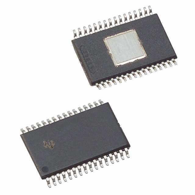
| 描述 | IC DUAL AUDIO DIFF RCVR 14-SOIC音频发送器、接收器、收发器 Audio Diff Line Receivers 0dB (G=1) |
| 产品分类 | 线性 - 音频处理集成电路 - IC |
| 品牌 | Texas Instruments |
| 产品手册 | |
| 产品图片 |
|
| rohs | 符合RoHS无铅 / 符合限制有害物质指令(RoHS)规范要求 |
| 产品系列 | 音频 IC,音频发送器、接收器、收发器,Texas Instruments INA2134UA- |
| 数据手册 | |
| 产品型号 | INA2134UA |
| 产品目录页面 | |
| 产品种类 | 音频发送器、接收器、收发器 |
| 供应商器件封装 | 14-SOIC |
| 制造商产品页 | http://www.ti.com/general/docs/suppproductinfo.tsp?distId=10&orderablePartNumber=INA2134UA |
| 包装 | 管件 |
| 单位重量 | 129.400 mg |
| 商标 | Texas Instruments |
| 安装类型 | 表面贴装 |
| 安装风格 | SMD/SMT |
| 封装 | Tube |
| 封装/外壳 | 14-SOIC(0.154",3.90mm 宽) |
| 封装/箱体 | SOIC-14 |
| 工作电源电压 | 4 V to 18 V |
| 工厂包装数量 | 50 |
| 应用 | 放大器,接收器 |
| 接收机数量 | 2 |
| 描述/功能 | differential line receivers consisting of high performance op amps |
| 最大工作温度 | + 85 C |
| 最小工作温度 | - 40 C |
| 标准包装 | 50 |
| 激励器数量 | 2 |
| 电源电流 | 2.4 mA |
| 类型 | 线路接收器 |
| 系列 | INA2134 |
| 通道数量 | 2 Channel |


PDF Datasheet 数据手册内容提取
® INA134 INA134 INA2134 INA2134 INA134 INA2134 AUDIO DIFFERENTIAL LINE RECEIVERS 0dB (G = 1) FEATURES APPLICATIONS l SINGLE AND DUAL VERSIONS l AUDIO DIFFERENTIAL LINE RECEIVER l LOW DISTORTION: 0.0005% at f = 1kHz l SUMMING AMPLIFIER l HIGH SLEW RATE: 14V/m s l UNITY-GAIN INVERTING AMPLIFIER l FAST SETTLING TIME: 3m s to 0.01% l PSUEDOGROUND GENERATOR l WIDE SUPPLY RANGE: – 4V to – 18V l INSTRUMENTATION BUILDING BLOCK l LOW QUIESCENT CURRENT: 2.9mA max l CURRENT SHUNT MONITOR l HIGH CMRR: 90dB l VOLTAGE-CONTROLLED CURRENT l FIXED GAIN = 0dB (1V/V) SOURCE l PACKAGES—SINGLE: 8-PIN DIP, SO-8 l GROUND LOOP ELIMINATOR DUAL: 14-PIN DIP, SO-14 V+ 7 DESCRIPTION 25kW 25kW 2 5 The INA134 and INA2134 are differential line receiv- –In Sense ers consisting of high performance op amps with on- chip precision resistors. They are fully specified for 6 Output high performance audio applications and have excel- lent ac specifications, including low distortion 25kW 25kW (0.0005% at 1kHz) and high slew rate (14V/m s), assur- +In 3 1 Ref ing good dynamic response. In addition, wide output INA134 V+ voltage swing and high output drive capability allow 4 11 use in a wide variety of demanding applications. The V– dual version features completely independent circuitry 2 25kW 25kW 12 –In A Sense A for lowest crosstalk and freedom from interaction, even when overdriven or overloaded. 13 A Out A The INA134 and INA2134 on-chip resistors are laser trimmed for accurate gain and optimum 25kW 25kW common-mode rejection. Furthermore, excellent TCR 3 14 +In A Ref A tracking of the resistors maintains gain accuracy and 25kW 25kW common-mode rejection over temperature. Operation 6 10 –In B Sense B is guaranteed from – 4V to – 18V (8V to 36V total supply). 9 B Out B The INA134 is available in 8-pin DIP and SO-8 surface-mount packages. The INA2134 comes in 25kW 25kW 14-pin DIP and SO-14 surface-mount packages. Both +In B 5 8 Ref B are specified for operation over the extended industrial INA2134 temperature range, –40(cid:176) C to +85(cid:176) C. 4 V– International Airport Industrial Park • Mailing Address: PO Box 11400, Tucson, AZ 85734 • Street Address: 6730 S. Tucson Blvd., Tucson, AZ 85706 • Tel: (520) 746-1111 • Twx: 910-952-1111 Internet: http://www.burr-brown.com/ • FAXLine: (800) 548-6133 (US/Canada Only) • Cable: BBRCORP • Telex: 066-6491 • FAX: (520) 889-1510 • Immediate Product Info: (800) 548-6132 ©1997 Burr-Brown Corporation PDS-1390A Printed in U.S.A. July, 1997 SBOS071
– SPECIFICATIONS: V = 18V S At T = +25(cid:176)C, V = – 18V, R = 2kW , and Ref Pin connected to Ground, unless otherwise noted. A S L INA134PA, UA INA2134PA, UA PARAMETER CONDITIONS MIN TYP MAX UNITS AUDIO PERFORMANCE Total Harmonic Distortion + Noise, f = 1kHz V = 10Vrms 0.0005 % IN Noise Floor(1) 20kHz BW –100 dBu Headroom(1) THD+N < 1% +23 dBu FREQUENCY RESPONSE Small-Signal Bandwidth 3.1 MHz Slew Rate 14 V/m s Settling Time: 0.1% 10V Step, C = 100pF 2 m s L 0.01% 10V Step, C = 100pF 3 m s L Overload Recovery Time 50% Overdrive 3 m s ChannelSeparation (dual), f = 1kHz 117 dB OUTPUT NOISE VOLTAGE(2) f = 20Hz to 20kHz 7 m Vrms f = 1kHz 52 nV/(cid:214) HZ OFFSET VOLTAGE(3) Input Offset Voltage V = 0V – 100 – 1000 m V CM vs Temperature Specified Temperature Range – 2 m V/(cid:176)C vs Power Supply V = – 4V to – 18V – 5 – 60 m V/V S INPUT Common-Mode Voltage Range: Positive V = 0V 2(V+)–5 2(V+)–4 V O Negative V = 0V 2(V–)+5 2(V–)+2 V O Differential Voltage Range See Typical Curve Common-Mode Rejection V = – 31V, R = 0W 74 90 dB CM S Impedance(4) Differential 50 kW Common-Mode 50 kW GAIN Initial 1 V/V Error V = –16V to 16V – 0.02 – 0.1 % O vs Temperature – 1 – 10 ppm/(cid:176)C Nonlinearity V = –16V to 16V 0.0001 % O OUTPUT Voltage Output, Positive (V+)–2 (V+)–1.8 V Negative (V–)+2 (V–)+1.6 V Current Limit, Continuous to Common – 60 mA Capacitive Load (Stable Operation) 500 pF POWER SUPPLY Rated Voltage – 18 V Voltage Range – 4 – 18 V Quiescent Current (per Amplifier) I = 0 – 2.4 – 2.9 mA O TEMPERATURE RANGE Specification Range –40 85 (cid:176)C Operation Range –55 125 (cid:176)C Storage Range –55 125 (cid:176)C Thermal Resistance, q JA 8-Pin DIP 100 (cid:176)C/W SO-8 Surface-Mount 150 (cid:176)C/W 14-Pin DIP 80 (cid:176)C/W SO-14 Surface-Mount 100 (cid:176)C/W NOTES: (1) dBu = 20log (Vrms/0.7746). (2) Includes effects of amplifier’s input current noise and thermal noise contribution of resistor network. (3) Includes effects of amplifier’s input bias and offset currents. (4) 25kW resistors are ratio matched but have – 25% absolute value. The information provided herein is believed to be reliable; however, BURR-BROWN assumes no responsibility for inaccuracies or omissions. BURR-BROWN assumes no responsibility for the use of this information, and all use of such information shall be entirely at the user’s own risk. Prices and specifications are subject to change without notice. No patent rights or licenses to any of the circuits described herein are implied or granted to any third party. BURR-BROWN does not authorize or warrant any BURR-BROWN product for use in life support devices and/or systems. ® INA134/2134 2
PIN CONFIGURATIONS Top View 8-Pin DIP/SO-8 Top View 14-Pin DIP/SO-14 Ref(cid:13) 1(cid:13) 8(cid:13) NC(cid:13) NC(cid:13) 1(cid:13) 14(cid:13) Ref A(cid:13) –In(cid:13) 2(cid:13) 7(cid:13) V+(cid:13) –In A(cid:13) 2(cid:13) 13(cid:13) Out A(cid:13) A +In(cid:13) 3(cid:13) 6(cid:13) Output(cid:13) +In A(cid:13) 3(cid:13) 12(cid:13) Sense A(cid:13) V– 4 5 Sense V–(cid:13) 4(cid:13) 11(cid:13) V+(cid:13) +In B(cid:13) 5(cid:13) 10(cid:13) Sense B(cid:13) NC = No Connection B –In B(cid:13) 6(cid:13) 9(cid:13) Out B(cid:13) ABSOLUTE MAXIMUM RATINGS(1) NC 7 8 Ref B Supply Voltage, V+ to V–....................................................................40V Input Voltage Range..........................................................................– 80V Output Short-Circuit (to ground)(2)...........................................Continuous Operating Temperature.................................................–55(cid:176)C to +125(cid:176)C NC = No Connection Storage Temperature.....................................................–55(cid:176)C to +125(cid:176)C Junction Temperature....................................................................+150(cid:176)C Lead Temperature (soldering, 10s)...............................................+300(cid:176)C NOTE: (1) Stresses above these ratings may cause permanent damage. ELECTROSTATIC (2) One channel per package. DISCHARGE SENSITIVITY PACKAGE/ORDERING INFORMATION This integrated circuit can be damaged by ESD. Burr-Brown PACKAGE SPECIFICATION recommends that all integrated circuits be handled with ap- DRAWING TEMPERATURE propriate precautions. Failure to observe proper handling and PRODUCT PACKAGE NUMBER(1) RANGE installation procedures can cause damage. Single INA134PA 8-Pin DIP 006 –40(cid:176)C to +85(cid:176)C ESD damage can range from subtle performance degradation INA134UA SO-8 Surface-Mount 182 –40(cid:176)C to +85(cid:176)C to complete device failure. Precision integrated circuits may Dual be more susceptible to damage because very small parametric INA2134PA 14-Pin DIP 010 –40(cid:176)C to +85(cid:176)C INA2134UA SO-14 Surface-Mount 235 –40(cid:176)C to +85(cid:176)C changes could cause the device not to meet its published specifications. NOTE: (1) For detailed drawing and dimension table, please see end of data sheet, or Appendix C of Burr-Brown IC Data Book. ® 3 INA134/2134
TYPICAL PERFORMANCE CURVES At T = +25(cid:176)C, V = – 18V, unless otherwise noted. A S TOTAL HARMONIC DISTORTION+NOISE(cid:13) DIM INTERMODULATION DISTORTION(cid:13) vs FREQUENCY vs OUTPUT AMPLITUDE 1(cid:13) 5(cid:13) BW = 100kHz V = 10Vrms O 0.1(cid:13) 1(cid:13) %) Noise ( 0.010(cid:13) R = 100kW M (%) 0.1(cid:13) RL = 2kW , 600W D+ L DI H R = 2kW T L 0.001(cid:13) 0.010(cid:13) R = 600W L 0.0001 0.001 20 100 1k 10k 20k –10 –5 0 5 10 15 20 25 Frequency (Hz) Output Amplitude (dBu) HEADROOM - TOTAL HARMONIC DISTORTION+NOISE(cid:13) HARMONIC DISTORTION PRODUCTS(cid:13) vs OUTPUT AMPLITUDE vs FREQUENCY 1(cid:13) 0.01(cid:13) f = 1kHz 0.1(cid:13) mental) 0.001(cid:13) 2nRdL H= a6r0m0oWn,i(cid:13)c R = 2kW ,(cid:13) 3RrdL H=a 6r0m0oWn,i(cid:13)c %) da 2ndL Harmonic e ( un +Nois 0.010(cid:13) RL = 600W % of F 0.0001(cid:13) THD de ( R = 2kW ,(cid:13) ( noise limited) 0.001(cid:13) RL = 2kW,(cid:13) mplitu 0.00001(cid:13) 3rd LHarmonic 100kW A V = 1Vrms O 0.0001 0.000001 0 5 10 15 20 25 30 20 100 1k 10k 20k Output Amplitude (dBu) Frequency (Hz) OUTPUT VOLTAGE NOISE SPECTRAL DENSITY(cid:13) OUTPUT NOISE VOLTAGE(cid:13) vs FREQUENCY vs NOISE BANDWIDTH 10k(cid:13) 100(cid:13) Hz) 1k(cid:13) ms) 10(cid:13) (cid:214)V/ Vr n µ e ( e ( s g Noi olta Voltage 100(cid:13) Noise V 1(cid:13) 10 0.1 1 10 100 1k 10k 100k 1M 1 10 100 1k 10k 100k Frequency (Hz) Frequency (Hz) ® INA134/2134 4
TYPICAL PERFORMANCE CURVES (CONT) At T = +25(cid:176)C, V = – 18V, unless otherwise noted. A S GAIN vs FREQUENCY COMMON-MODE REJECTION vs FREQUENCY 10(cid:13) 100(cid:13) B) 80(cid:13) d 0(cid:13) n ( n (dB) ejectio 60(cid:13) Gai –10(cid:13) e R age Mod 40(cid:13) olt n- V –20(cid:13) mo m 20(cid:13) o C –30 0 1k 10k 100k 1M 10M 1k 10k 100k 1M Frequency (Hz) Frequency (Hz) POWER SUPPLY REJECTION vs FREQUENCY CHANNEL SEPARATION vs FREQUENCY 120(cid:13) 130(cid:13) R = 100kW B) 100(cid:13) L Rejection (d 8600(cid:13)(cid:13) –PSR aration (dB) 112100(cid:13)(cid:13) RL = 2kW y ep pl S Sup 40(cid:13) nel ower 20(cid:13) +PSR Chan 100(cid:13) P 0 90 100 1k 10k 100k 1M 20 100 1k 10k 20k Frequency (Hz) Frequency (Hz) INPUT COMMON-MODE VOLTAGE RANGE(cid:13) MAXIMUM OUTPUT VOLTAGE vs FREQUENCY vs OUTPUT VOLTAGE 40(cid:13) 40(cid:13) V = ±18V S 30(cid:13) V) 20(cid:13) p) 30(cid:13) e ( e (Vp- Voltag 100(cid:13)(cid:13) ag 20(cid:13) e olt od –10(cid:13) V M put on- –20(cid:13) Out 10(cid:13) mm –30(cid:13) o C V = 0V(cid:13) –40(cid:13) REF R = 2kW L 0 –50 100 1k 10k 100k 1M 10M –20 –15 –10 –5 0 5 10 15 20 Frequency (Hz) Output Voltage (V) ® 5 INA134/2134
TYPICAL PERFORMANCE CURVES (CONT) At T = +25(cid:176)C, V = – 18V, unless otherwise noted. A S QUIESCENT CURRENT vs TEMPERATURE SLEW RATE vs TEMPERATURE 4(cid:13) 16(cid:13) –SR A) 3(cid:13) 14(cid:13) ent (m V/µs) +SR urr 2(cid:13) e ( 12(cid:13) C at ent w R uiesc 1(cid:13) Sle 10(cid:13) Q 0 8 –75 –50 –25 0 25 50 75 100 125 –75 –50 –25 0 25 50 75 100 125 Temperature (°C) Temperature (°C) SHORT-CIRCUIT CURRENT vs TEMPERATURE QUIESCENT CURRENT vs SUPPLY VOLTAGE 80(cid:13) 3(cid:13) 60(cid:13) mA) 40(cid:13) +I A) Current ( 200(cid:13)(cid:13) SC urrent (m 2(cid:13) ort-Circuit ––2400(cid:13)(cid:13) –ISC uiescent C 1(cid:13) h Q S –60(cid:13) –80 0 –75 –50 –25 0 25 50 75 100 125 ±4 ±6 ±8 ±10 ±12 ±14 ±16 ±18 Temperature (°C) Supply Voltage (V) OFFSET VOLTAGE(cid:13) OFFSET VOLTAGE DRIFT(cid:13) PRODUCTION DISTRIBUTION PRODUCTION DISTRIBUTION 25(cid:13) 25(cid:13) Typical Production(cid:13) Typical Production Distribution(cid:13) Distribution of(cid:13) Packaged Units. of Packaged Units. %) 20(cid:13) %) 20(cid:13) s ( s ( plifier 15(cid:13) plifier 15(cid:13) m m A A of 10(cid:13) of 10(cid:13) nt nt e e c c er er P 5(cid:13) P 5(cid:13) 0 0 0(cid:13)0(cid:13)0(cid:13)0(cid:13)0(cid:13)0(cid:13)0(cid:13)0(cid:13)0(cid:13)0(cid:13)0(cid:13)0(cid:13)0(cid:13)0(cid:13)0(cid:13)0(cid:13)0(cid:13)0(cid:13)0(cid:13)0(cid:13)0 0(cid:13)5(cid:13)1(cid:13)5(cid:13)2(cid:13)5(cid:13)3(cid:13)5(cid:13)4(cid:13)5(cid:13)5(cid:13)5(cid:13)6(cid:13)5(cid:13)7(cid:13)5(cid:13)8(cid:13)5(cid:13)9(cid:13)5(cid:13)0(cid:13)5(cid:13)1(cid:13)5(cid:13)2 100–90–80–70–60–50–40–30–20–10 102030405060708090100 0. 1. 2. 3. 4. 5. 6. 7. 8. 9.110.111.1 – Offset Voltage (µV) Offset Voltage Drift (µV/°C) ® INA134/2134 6
TYPICAL PERFORMANCE CURVES (CONT) At T = +25(cid:176)C, V = – 18V, unless otherwise noted. A S (cid:13) SMALL-SIGNAL OVERSHOOT(cid:13) OUTPUT VOLTAGE SWING vs OUTPUT CURRENT vs LOAD CAPACITANCE 17(cid:13) 70(cid:13) 16(cid:13) –55°C 60(cid:13) 15(cid:13) V) 25°C wing ( 1143(cid:13)(cid:13) 125°C %) 50(cid:13) utput Voltage S –––11112234(cid:13)(cid:13)(cid:13) 85°1C25°C 85°C Overshoot ( 432000(cid:13)(cid:13)(cid:13) O –15(cid:13) (cid:13) R = 2kW (cid:13) –16(cid:13) 25°C –55°C 10(cid:13) 100LmV Step –17(cid:13) 0 (cid:13) 0 ±20 ±40 ±60 ±80 ±100 0 400 800 1200 1600 2000 Output Current (mA) Load Capacitance (pF) LARGE-SIGNAL STEP RESPONSE C = 500pF SMALL-SIGNAL STEP RESPONSE L C = 100pF L v di v mV/ V/di 0 5 5 C = 500pF L 1m s/div 1m s/div ® 7 INA134/2134
APPLICATIONS INFORMATION V– V+ Figure 1 shows the basic connections required for operation of the INA134. Decoupling capacitors are strongly recom- 1µF 1µF mended in applications with noisy or high impedance power supplies. The capacitors should be placed close to the device 4 7 pins as shown in Figure 1. All circuitry is completely INA134 independent in the dual version assuring lowest crosstalk R1(cid:13) R2(cid:13) –In 25kW 25kW and normal behavior when one amplifier is overdriven or 2 5 V 2 short-circuited. As shown in Figure 1, the differential input signal is con- nected to pins 2 and 3. The source impedances connected to 6 the inputs must be nearly equal to assure good common- V = V –V OUT 3 2 mode rejection. A 10W mismatch in source impedance will R R 3(cid:13) 4(cid:13) degrade the common-mode rejection of a typical device to +In 25kW 25kW 3 1 approximately 74dB. If the source has a known impedance V3 mismatch, an additional resistor in series with the opposite input can be used to preserve good common-mode rejection. Do not interchange pins 1 and 3 or pins 2 and 5, even though FIGURE 1. Precision Difference Amplifier (Basic Power nominal resistor values are equal. These resistors are laser Supply and Signal Connections). trimmed for precise resistor ratios to achieve accurate gain and highest CMR. Interchanging these pins would not pro- vide specified performance. INA134 AUDIO PERFORMANCE R R 1 2 The INA134 and INA2134 were designed for enhanced ac 2 5 V 2 performance. Very low distortion, low noise, and wide band- width provide superior performance in high quality audio applications. Laser-trimmed matched resistors provide opti- 6 V O mum common-mode rejection (typically 90dB), especially when compared to circuits implemented with an op amp and 10W R 3 discrete precision resistors. In addition, high slew rate 3 V (14V/m s) and fast settling time (3m s to 0.01%) ensure good 3 dynamic performance. R 4 The INA134 and INA2134 have excellent distortion charac- +15V teristics. THD+Noise is below 0.002% throughout the audio 1 frequency range. Up to approximately 10kHz distortion is VO = V3 – V2(cid:13) 499kW below the measurement limit of commonly used test equip- Offset Adjustment(cid:13) 100kW Range = ±300µV ment. Furthermore, distortion remains relatively flat over its 10W wide output voltage swing range (approximately 1.7V from either supply). –15V OFFSET VOLTAGE TRIM FIGURE 2. Offset Adjustment. The INA134 and INA2134 are laser trimmed for low offset voltage and drift. Most applications require no external offset adjustment. Figure 2 shows an optional circuit for trimming the output offset voltage. The output is referred to the output reference terminal (pin 1), which is normally grounded. A voltage applied to the Ref terminal will be summed with the output signal. This can be used to null offset voltage as shown in Figure 2. The source impedance of a signal applied to the Ref terminal should be less than 10W to maintain good common-mode rejection. ® INA134/2134 8
INA134 2 5 INA134 V 1 6 V = V + V –In 1/2(cid:13) 2 5 1 0 1 2 OPA2134 V 1 R 2 V 2 3 6 R 1 V(cid:13) FIGURE 3. Precision Summing Amplifier. R2 0utp0ut 1/2(cid:13) 3 1 V OPA2134 2 INA134 +In 2 5 –In V = (1 + 2R/R) (V –V) O 2 1 2 1 6 3 6 BUF634 VO FIGURE 5. High Input Impedance Instrumentation Amplifier. 3 1 +In FIGURE 4. Boosting Output Current. The difference amplifier is a highly versatile building •Precision Summing Instrumentation Amplifier block that is useful in a wide variety of applications. See •Precision Absolute Value Buffer the INA105 data sheet for additional applications ideas, •Precision Voltage-to-Current Converter with Differential including: Inputs •Current Receiver with Compliance to Rails •Differential Input Voltage-to-Current Converter for Low •Precision Unity-Gain Inverting Amplifier I OUT •– 10V Precision Voltage Reference •Isolating Current Source •– 5V Precision Voltage Reference •Differential Output Difference Amplifier •Precision Unity-Gain Buffer •Isolating Current Source with Buffering Amplifier for Greater Accuracy •Precision Average Value Amplifier •Precision G = 2 Amplifier •Window Comparator with Window Span and Window Center Inputs •Precision Summing Amplifier •Precision Voltage-Controlled Current Source with Buff- •Precision G = 1/2 Amplifier ered Differential Inputs and Gain •Precision Bipolar Offsetting •Digitally Controlled Gain of – 1 Amplifier •Precision Summing Amplifier with Gain •Instrumentation Amplifier Guard Drive Generator ® 9 INA134/2134
PACKAGE OPTION ADDENDUM www.ti.com 6-Feb-2020 PACKAGING INFORMATION Orderable Device Status Package Type Package Pins Package Eco Plan Lead/Ball Finish MSL Peak Temp Op Temp (°C) Device Marking Samples (1) Drawing Qty (2) (6) (3) (4/5) INA134PA ACTIVE PDIP P 8 50 Green (RoHS NIPDAU N / A for Pkg Type INA134PA & no Sb/Br) INA134UA ACTIVE SOIC D 8 75 Green (RoHS NIPDAU Level-3-260C-168 HR -40 to 85 INA & no Sb/Br) 134UA INA134UA/2K5 ACTIVE SOIC D 8 2500 Green (RoHS NIPDAU Level-3-260C-168 HR -40 to 85 INA & no Sb/Br) 134UA INA134UA/2K5E4 ACTIVE SOIC D 8 2500 Green (RoHS NIPDAU Level-3-260C-168 HR -40 to 85 INA & no Sb/Br) 134UA INA134UAE4 ACTIVE SOIC D 8 75 Green (RoHS NIPDAU Level-3-260C-168 HR -40 to 85 INA & no Sb/Br) 134UA INA2134PA ACTIVE PDIP N 14 25 Green (RoHS NIPDAU N / A for Pkg Type INA2134PA & no Sb/Br) INA2134UA ACTIVE SOIC D 14 50 Green (RoHS NIPDAU Level-3-260C-168 HR -40 to 85 INA2134UA & no Sb/Br) INA2134UA/2K5 ACTIVE SOIC D 14 2500 Green (RoHS NIPDAU Level-3-260C-168 HR -40 to 85 INA2134UA & no Sb/Br) INA2134UA/2K5E4 ACTIVE SOIC D 14 2500 Green (RoHS NIPDAU Level-3-260C-168 HR -40 to 85 INA2134UA & no Sb/Br) INA2134UA/2K5G4 ACTIVE SOIC D 14 2500 Green (RoHS NIPDAU Level-3-260C-168 HR -40 to 85 INA2134UA & no Sb/Br) INA2134UAE4 ACTIVE SOIC D 14 50 Green (RoHS NIPDAU Level-3-260C-168 HR -40 to 85 INA2134UA & no Sb/Br) (1) The marketing status values are defined as follows: ACTIVE: Product device recommended for new designs. LIFEBUY: TI has announced that the device will be discontinued, and a lifetime-buy period is in effect. NRND: Not recommended for new designs. Device is in production to support existing customers, but TI does not recommend using this part in a new design. PREVIEW: Device has been announced but is not in production. Samples may or may not be available. OBSOLETE: TI has discontinued the production of the device. (2) RoHS: TI defines "RoHS" to mean semiconductor products that are compliant with the current EU RoHS requirements for all 10 RoHS substances, including the requirement that RoHS substance do not exceed 0.1% by weight in homogeneous materials. Where designed to be soldered at high temperatures, "RoHS" products are suitable for use in specified lead-free processes. TI may reference these types of products as "Pb-Free". RoHS Exempt: TI defines "RoHS Exempt" to mean products that contain lead but are compliant with EU RoHS pursuant to a specific EU RoHS exemption. Green: TI defines "Green" to mean the content of Chlorine (Cl) and Bromine (Br) based flame retardants meet JS709B low halogen requirements of <=1000ppm threshold. Antimony trioxide based flame retardants must also meet the <=1000ppm threshold requirement. Addendum-Page 1
PACKAGE OPTION ADDENDUM www.ti.com 6-Feb-2020 (3) MSL, Peak Temp. - The Moisture Sensitivity Level rating according to the JEDEC industry standard classifications, and peak solder temperature. (4) There may be additional marking, which relates to the logo, the lot trace code information, or the environmental category on the device. (5) Multiple Device Markings will be inside parentheses. Only one Device Marking contained in parentheses and separated by a "~" will appear on a device. If a line is indented then it is a continuation of the previous line and the two combined represent the entire Device Marking for that device. (6) Lead/Ball Finish - Orderable Devices may have multiple material finish options. Finish options are separated by a vertical ruled line. Lead/Ball Finish values may wrap to two lines if the finish value exceeds the maximum column width. Important Information and Disclaimer:The information provided on this page represents TI's knowledge and belief as of the date that it is provided. TI bases its knowledge and belief on information provided by third parties, and makes no representation or warranty as to the accuracy of such information. Efforts are underway to better integrate information from third parties. TI has taken and continues to take reasonable steps to provide representative and accurate information but may not have conducted destructive testing or chemical analysis on incoming materials and chemicals. TI and TI suppliers consider certain information to be proprietary, and thus CAS numbers and other limited information may not be available for release. In no event shall TI's liability arising out of such information exceed the total purchase price of the TI part(s) at issue in this document sold by TI to Customer on an annual basis. OTHER QUALIFIED VERSIONS OF INA2134 : •Enhanced Product: INA2134-EP NOTE: Qualified Version Definitions: •Enhanced Product - Supports Defense, Aerospace and Medical Applications Addendum-Page 2
PACKAGE MATERIALS INFORMATION www.ti.com 24-Jul-2013 TAPE AND REEL INFORMATION *Alldimensionsarenominal Device Package Package Pins SPQ Reel Reel A0 B0 K0 P1 W Pin1 Type Drawing Diameter Width (mm) (mm) (mm) (mm) (mm) Quadrant (mm) W1(mm) INA134UA/2K5 SOIC D 8 2500 330.0 12.4 6.4 5.2 2.1 8.0 12.0 Q1 INA2134UA/2K5 SOIC D 14 2500 330.0 16.4 6.5 9.0 2.1 8.0 16.0 Q1 PackMaterials-Page1
PACKAGE MATERIALS INFORMATION www.ti.com 24-Jul-2013 *Alldimensionsarenominal Device PackageType PackageDrawing Pins SPQ Length(mm) Width(mm) Height(mm) INA134UA/2K5 SOIC D 8 2500 367.0 367.0 35.0 INA2134UA/2K5 SOIC D 14 2500 367.0 367.0 38.0 PackMaterials-Page2
None
None
PACKAGE OUTLINE D0008A SOIC - 1.75 mm max height SCALE 2.800 SMALL OUTLINE INTEGRATED CIRCUIT C SEATING PLANE .228-.244 TYP [5.80-6.19] .004 [0.1] C A PIN 1 ID AREA 6X .050 [1.27] 8 1 2X .189-.197 [4.81-5.00] .150 NOTE 3 [3.81] 4X (0 -15 ) 4 5 8X .012-.020 B .150-.157 [0.31-0.51] .069 MAX [3.81-3.98] .010 [0.25] C A B [1.75] NOTE 4 .005-.010 TYP [0.13-0.25] 4X (0 -15 ) SEE DETAIL A .010 [0.25] .004-.010 0 - 8 [0.11-0.25] .016-.050 [0.41-1.27] DETAIL A (.041) TYPICAL [1.04] 4214825/C 02/2019 NOTES: 1. Linear dimensions are in inches [millimeters]. Dimensions in parenthesis are for reference only. Controlling dimensions are in inches. Dimensioning and tolerancing per ASME Y14.5M. 2. This drawing is subject to change without notice. 3. This dimension does not include mold flash, protrusions, or gate burrs. Mold flash, protrusions, or gate burrs shall not exceed .006 [0.15] per side. 4. This dimension does not include interlead flash. 5. Reference JEDEC registration MS-012, variation AA. www.ti.com
EXAMPLE BOARD LAYOUT D0008A SOIC - 1.75 mm max height SMALL OUTLINE INTEGRATED CIRCUIT 8X (.061 ) [1.55] SYMM SEE DETAILS 1 8 8X (.024) [0.6] SYMM (R.002 ) TYP [0.05] 5 4 6X (.050 ) [1.27] (.213) [5.4] LAND PATTERN EXAMPLE EXPOSED METAL SHOWN SCALE:8X SOLDER MASK SOLDER MASK METAL OPENING OPENING METAL UNDER SOLDER MASK EXPOSED METAL EXPOSED METAL .0028 MAX .0028 MIN [0.07] [0.07] ALL AROUND ALL AROUND NON SOLDER MASK SOLDER MASK DEFINED DEFINED SOLDER MASK DETAILS 4214825/C 02/2019 NOTES: (continued) 6. Publication IPC-7351 may have alternate designs. 7. Solder mask tolerances between and around signal pads can vary based on board fabrication site. www.ti.com
EXAMPLE STENCIL DESIGN D0008A SOIC - 1.75 mm max height SMALL OUTLINE INTEGRATED CIRCUIT 8X (.061 ) [1.55] SYMM 1 8 8X (.024) [0.6] SYMM (R.002 ) TYP [0.05] 5 4 6X (.050 ) [1.27] (.213) [5.4] SOLDER PASTE EXAMPLE BASED ON .005 INCH [0.125 MM] THICK STENCIL SCALE:8X 4214825/C 02/2019 NOTES: (continued) 8. Laser cutting apertures with trapezoidal walls and rounded corners may offer better paste release. IPC-7525 may have alternate design recommendations. 9. Board assembly site may have different recommendations for stencil design. www.ti.com
None
None
IMPORTANTNOTICEANDDISCLAIMER TI PROVIDES TECHNICAL AND RELIABILITY DATA (INCLUDING DATASHEETS), DESIGN RESOURCES (INCLUDING REFERENCE DESIGNS), APPLICATION OR OTHER DESIGN ADVICE, WEB TOOLS, SAFETY INFORMATION, AND OTHER RESOURCES “AS IS” AND WITH ALL FAULTS, AND DISCLAIMS ALL WARRANTIES, EXPRESS AND IMPLIED, INCLUDING WITHOUT LIMITATION ANY IMPLIED WARRANTIES OF MERCHANTABILITY, FITNESS FOR A PARTICULAR PURPOSE OR NON-INFRINGEMENT OF THIRD PARTY INTELLECTUAL PROPERTY RIGHTS. These resources are intended for skilled developers designing with TI products. You are solely responsible for (1) selecting the appropriate TI products for your application, (2) designing, validating and testing your application, and (3) ensuring your application meets applicable standards, and any other safety, security, or other requirements. These resources are subject to change without notice. TI grants you permission to use these resources only for development of an application that uses the TI products described in the resource. Other reproduction and display of these resources is prohibited. No license is granted to any other TI intellectual property right or to any third party intellectual property right. TI disclaims responsibility for, and you will fully indemnify TI and its representatives against, any claims, damages, costs, losses, and liabilities arising out of your use of these resources. TI’s products are provided subject to TI’s Terms of Sale (www.ti.com/legal/termsofsale.html) or other applicable terms available either on ti.com or provided in conjunction with such TI products. TI’s provision of these resources does not expand or otherwise alter TI’s applicable warranties or warranty disclaimers for TI products. Mailing Address: Texas Instruments, Post Office Box 655303, Dallas, Texas 75265 Copyright © 2020, Texas Instruments Incorporated