ICGOO在线商城 > 集成电路(IC) > 线性 - 音頻放大器 > TAS5615DKD
 Datasheet下载
- 型号: TAS5615DKD
- 制造商: Texas Instruments
- 库位|库存: xxxx|xxxx
- 要求:
| 数量阶梯 | 香港交货 | 国内含税 |
| +xxxx | $xxxx | ¥xxxx |
查看当月历史价格
查看今年历史价格
TAS5615DKD产品简介:
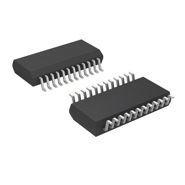
ICGOO电子元器件商城为您提供TAS5615DKD由Texas Instruments设计生产,在icgoo商城现货销售,并且可以通过原厂、代理商等渠道进行代购。 TAS5615DKD价格参考。Texas InstrumentsTAS5615DKD封装/规格:线性 - 音頻放大器, Amplifier IC 1-Channel (Mono) or 2-Channel (Stereo) Class D 44-HSSOP。您可以下载TAS5615DKD参考资料、Datasheet数据手册功能说明书,资料中有TAS5615DKD 详细功能的应用电路图电压和使用方法及教程。
TAS5615DKD是德州仪器(Texas Instruments)推出的一款高效D类音频功率放大器,属于线性-音频放大器类别。该器件广泛应用于需要高效率、高功率输出和优良音质的音频系统中。

典型应用场景包括:家用音响系统、有源音箱、迷你音响、多媒体音箱以及电视外置音响等。TAS5615DKD采用BTL(桥接负载)输出结构,支持多通道配置,可提供高达数百瓦的功率输出,适合驱动低阻抗扬声器,实现强劲、清晰的音频表现。

其内置的高效调制技术和先进保护功能(如过流、过热和短路保护),确保了系统在长时间运行下的稳定性和可靠性。此外,该芯片支持多级电源电压管理,可在不同供电条件下优化性能与功耗,适用于对能效要求较高的产品设计。

TAS5615DKD常用于数字音频接收后端,配合DSP或音频处理器使用,广泛见于中高端消费类音频设备和专业音响系统中。其高集成度和优异的音频性能,使其成为追求高保真音效与紧凑设计产品的理想选择。
| 参数 | 数值 |
| 产品目录 | 集成电路 (IC)半导体 |
| 描述 | IC AMP AUDIO 160W STER D 44HSSOP音频放大器 Ana inp 150W Stereo class D Amplifier |
| 产品分类 | |
| 品牌 | Texas Instruments |
| 产品手册 | http://www.ti.com/lit/gpn/tas5615 |
| 产品图片 |
|
| rohs | 符合RoHS无铅 / 符合限制有害物质指令(RoHS)规范要求 |
| 产品系列 | 音频 IC,音频放大器,Texas Instruments TAS5615DKDPurePath™ HD |
| 数据手册 | |
| 产品型号 | TAS5615DKD |
| Pd-功率耗散 | 2.3 W |
| THD+噪声 | 0.05 % |
| 不同负载时的最大输出功率x通道数 | 300W x 1 @ 4 欧姆; 160W x 2 @ 8 欧姆 |
| 产品 | Audio Amplifiers |
| 产品目录页面 | |
| 产品种类 | 音频放大器 |
| 供应商器件封装 | 44-HSSOP |
| 其它名称 | 296-24654-5 |
| 包装 | 管件 |
| 双重电源电压 | 12 V, 50 V |
| 商标 | Texas Instruments |
| 增益 | 23 dB |
| 安装类型 | 表面贴装 |
| 安装风格 | SMD/SMT |
| 封装 | Tube |
| 封装/外壳 | 44-BSSOP(0.433",11.00mm 宽)裸焊盘 |
| 封装/箱体 | HSSOP-44 |
| 工作温度 | 0°C ~ 70°C (TA) |
| 工厂包装数量 | 29 |
| 最大功率耗散 | 2.3 W |
| 最大工作温度 | + 70 C |
| 最小工作温度 | 0 C |
| 标准包装 | 29 |
| 特性 | 消除爆音,差分输入,短路和热保护,关闭 |
| 电压-电源 | 25 V ~ 52.5 V |
| 电源电流 | 22.5 mA, 8 mA |
| 电源类型 | Triple |
| 类 | Class-D |
| 类型 | 1-Channel Mono or 2-Channel Stereo or 4-Channel Stereo |
| 系列 | TAS5615 |
| 输入信号类型 | Differential, Single |
| 输出信号类型 | Differential, Single |
| 输出功率 | 300 W |
| 输出类型 | 1-通道(单声道)或 2-通道(立体声) |
| 音频负载电阻 | 8 Ohms |


- 商务部:美国ITC正式对集成电路等产品启动337调查
- 曝三星4nm工艺存在良率问题 高通将骁龙8 Gen1或转产台积电
- 太阳诱电将投资9.5亿元在常州建新厂生产MLCC 预计2023年完工
- 英特尔发布欧洲新工厂建设计划 深化IDM 2.0 战略
- 台积电先进制程称霸业界 有大客户加持明年业绩稳了
- 达到5530亿美元!SIA预计今年全球半导体销售额将创下新高
- 英特尔拟将自动驾驶子公司Mobileye上市 估值或超500亿美元
- 三星加码芯片和SET,合并消费电子和移动部门,撤换高东真等 CEO
- 三星电子宣布重大人事变动 还合并消费电子和移动部门
- 海关总署:前11个月进口集成电路产品价值2.52万亿元 增长14.8%


PDF Datasheet 数据手册内容提取
PurePath Digital TAS5615 www.ti.com SLAS595B–JUNE2009–REVISEDFEBRUARY2010 160 W STEREO/300W MONO PurePath™ HD Analog-Input Power Stage CheckforSamples:TAS5615 FEATURES 1 DESCRIPTION • ActiveEnabledIntegratedFeedbackProvides: 23 (PurePath™HDTechnology) The TAS5615 is a high-performance analog input – SignalBandwidthupto80kHzfor class-D amplifier with integrated closed-loop High-FrequencyContentFrom feedback technology (known as PurePath™ HD High-DefinitionSources technology). It has the ability to drive up to 160 W(1) stereo into 8-Ω speakers from a single 50-V – Ultralow0.03%THDat1Winto8Ω supply. – 0.03%THDAcrossAllFrequenciesfor PurePath HD technology enables traditional NaturalSoundat1W AB-amplifier performance (<0.03% THD) levels while – 80-dBPSRR(BTL,NoInputSignal) providing the power efficiency of traditional class-D – >100-dB(Aweighted)SNR amplifiers. – Click-andPop-FreeStart-Up Ultralow 0.03% THD+N is flat across all frequencies, – MinimalExternalComponentsComparedto ensuring that the amplifier does not add uneven DiscreteSolutions distortioncharacteristics,andhelpsmaintainanatural sound. • MultipleConfigurationsPossibleontheSame PCB: The efficiency of this class-D amplifier is greater than 90%. Undervoltage protection, overtemperature, – MonoParallelBridge-TiedLoad(PBTL) clipping, short-circuit and overcurrent protection are – 2.1Single-Ended(SE)StereoPairand all integrated, safeguarding the device and speakers Bridge-TiedLoad(BTL)Subwoofer against fault conditions that could damage the – QuadSingle-Ended(SE)Outputs system. • TotalOutputPowerat10%THD+N 3´OPA1632 – 300WinMonoPBTLConfiguration ♫♪ – 160WperChannelinStereoBTL – 80WperChannelinQuadSingle-Ended ANAAULDOIOG PurTeAPSat5h6T1M5HD ♫♪ INPUT (2.1 Configuration) • HighEfficiencyPowerStage(>90%)With120 ♫♪ mΩ OutputMOSFETs • TwoThermallyEnhancedPackageOptions: ±15 V 12V 25V–50 V – PHD(64-PinQFP) PurePathTMHD – DKD(44-PinPSOP3) Class-G Power Supply Ref. Design • Self-ProtectionDesign(Including Undervoltage,Overtemperature,Clipping,and Short-CircuitProtection)WithErrorReporting 110VAC®240 VAC • EMICompliantWhenUsedWith RecommendedSystemDesign APPLICATIONS • MiniComboSystem (1) Achievableoutputpowerlevelsaredependentonthethermal • AVReceivers configurationofthetargetapplication.Ahighperformance thermalinterfacematerialbetweenthepackageexposed • DVDReceivers heatslugandtheheatsinkshouldbeusedtoachievehigh • ActiveSpeakers outputpowerlevels 1 Pleasebeawarethatanimportantnoticeconcerningavailability,standardwarranty,anduseincriticalapplicationsofTexas Instrumentssemiconductorproductsanddisclaimerstheretoappearsattheendofthisdatasheet. PurePathHDisatrademarkofTexasInstruments. 2 Allothertrademarksarethepropertyoftheirrespectiveowners. 3 PRODUCTIONDATAinformationiscurrentasofpublicationdate. Copyright©2009–2010,TexasInstrumentsIncorporated Products conform to specifications per the terms of the Texas Instruments standard warranty. Production processing does not necessarilyincludetestingofallparameters.
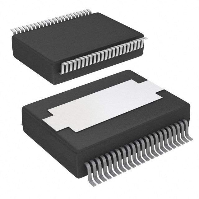
TAS5615 SLAS595B–JUNE2009–REVISEDFEBRUARY2010 www.ti.com Thesedeviceshavelimitedbuilt-inESDprotection.Theleadsshouldbeshortedtogetherorthedeviceplacedinconductivefoam duringstorageorhandlingtopreventelectrostaticdamagetotheMOSgates. DEVICE INFORMATION Terminal Assignment TheTAS5615isavailableintwothermallyenhancedpackages:PurePathHD™ • 64-PinQFP(PHD)PowerPackage • 44-PinPSOP3package(DKD) The package type contains a heat slug that is located on the top side of the device for convenient thermal couplingtotheheatsink. PHD PACKAGE DKD PACKAGE (TOPVIEW) (TOPVIEW) VDDPSU_REFNCNCNCNCGNDGNDGVDD_BGVDD_ABST_AOUT_AOUT_APVDD_APVDD_AGND_A PSU_REF 1 44 GVDD_AB VDD 2 43 BST_A OC_ADJ 3 42 PVDD_A 4321098765432109 RESET 4 41 PVDD_A ORCE_SAEDTJ 2166666555555555544478 GGNNDD__AB C_STARTUP 5 40 OUT_A C_STARTUP 3 46 GND_B INPUT_A 6 39 OUT_A INPUT_A 4 45 OUT_B INPUT_B 7 38 GND_A INPUT_B 5 44 OUT_B VI_CM 8 37 GND_B VI_CM 6 43 PVDD_B GND 7 42 PVDD_B GND 9 4 36 OUT_B IINNPPAVUUGRTTNE__CDGD 119810 33448901 PPBBVVSSDDTT__DDCB__CC INPAVUGRTNE_CGD 111102 (TOPV4pinsPA 333543 BPBSVSTDT__DBC_B FREQ_ADJ 12 37 OUT_C INPUT_D 13 IEWCK 32 PVDD_C OOSSCC__IISOOD+- 111543 64-pins QFPpackage 333456 GGONNUDDT___CCC FROESQC__AIOD+J 1145 )AGE 3310 GONUDT__CC OTW1 16 33 GND_D OSC_IO- 16 29 GND_D 17181920212223242526272829303132 SD 17 28 OUT_D OTW 18 27 OUT_D READY 19 26 PVDD_D OTW2CLIPREADYM1M2M3GNDGNDVDD_CVDD_DBST_DOUT_DOUT_DVDD_DVDD_DGND_D MM21 2201 2254 PBVSDT_DD_D GG PP M3 22 23 GVDD_CD PIN ONE LOCATION PHD PACKAGE Electrical Pin 1 Pin 1 Marker White Dot 2 SubmitDocumentationFeedback Copyright©2009–2010,TexasInstrumentsIncorporated ProductFolderLink(s):TAS5615
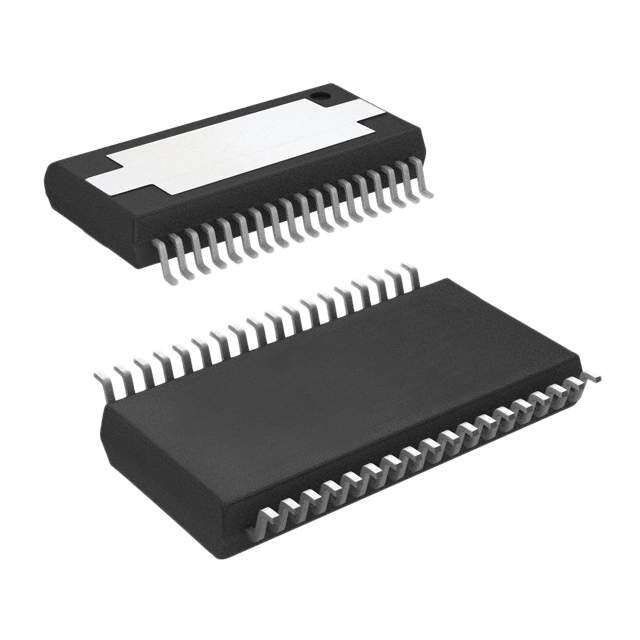
TAS5615 www.ti.com SLAS595B–JUNE2009–REVISEDFEBRUARY2010 MODE SELECTION PINS MODEPINS ANALOG OUTPUT DESCRIPTION M3 M2 M1 INPUT CONFIGURATION 0 0 0 Differential 2×BTL ADmode 0 0 1 — — Reserved 0 1 0 Differential 2×BTL BDmode Differential 0 1 1 1×BTL+2×SE ADmode,BTLdifferential Single-ended 1 0 0 Single-ended 4×SE ADmode INPUT_C(1) INPUT_D(1) 1 0 1 Differential 1×PBTL 0 0 ADmode 1 0 BDmode 1 1 0 Reserved 1 1 1 (1) INPUT_Cand_DareusedtoselectbetweenasubsetofADandBDmodeoperationsinPBTLmode(1=VREGand0=AGND). PACKAGE HEAT DISSIPATION RATINGS(1) PARAMETER TAS5615PHD TAS5615DKD R (°C/W)–2BTLor4SEchannels 3.63 2.52 qJC R (°C/W)–1BTLor2SEchannel(s) 5.95 3.22 qJC R (°C/W)–1SEchannel 9.9 6.9 qJC Padarea (2) 49mm2 80mm2 (1) J isjunction-to-case,CHiscase-to-heatsink C (2) R isanimportantconsideration.Assumea2-milthicknessoftypicalthermalgreasebetweenthepadareaandtheheatsinkandboth qH channelsactive.TheR withthisconditionis1.22°C/WforthePHDpackageand1.02°C/WfortheDKDpackage. qCH Table1. ORDERINGINFORMATION(1) T PACKAGE DESCRIPTION A 0°C–70°C TAS5615PHD 64-pinHTQFP 0°C–70°C TAS5615DKD 44-pinPSOP3 (1) Forthemostcurrentpackageandorderinginformation,seethePackageOptionAddendumattheendofthisdocument,orseetheTI Websiteatwww.ti.com. Copyright©2009–2010,TexasInstrumentsIncorporated SubmitDocumentationFeedback 3 ProductFolderLink(s):TAS5615
TAS5615 SLAS595B–JUNE2009–REVISEDFEBRUARY2010 www.ti.com ABSOLUTE MAXIMUM RATINGS overoperatingfree-airtemperaturerangeunlessotherwisenoted (1) TAS5615 UNIT VDDtoAGND –0.3to13.2 V GVDDtoAGND –0.3to13.2 V PVDD_XtoGND_X(2) –0.3to69.0 V OUT_XtoGND_X(2) –0.3to69.0 V BST_XtoGND_X(2) –0.3to82.2 V BST_XtoGVDD_X(2) –0.3to69.0 V VREGtoAGND –0.3to4.2 V GND_XtoGND –0.3to0.3 V GND_XtoAGND –0.3to0.3 V OC_ADJ,M1,M2,M3,OSC_IO+,OSC_IO–,FREQ_ADJ,VI_CM,C_STARTUP, –0.3to4.2 V PSU_REFtoAGND INPUT_X –0.3to5 V RESET,SD,OTW1,OTW2,CLIP,READYtoAGND –0.3to7.0 V Continuoussinkcurrent(SD,OTW1,OTW2,CLIP,READY) 9 mA Operatingjunctiontemperaturerange,T 0to150 °C J Storagetemperature,T –40to150 °C stg Human-bodymodel(3)(allpins) ±2 kV Electrostaticdischarge Charged-devicemodel(3)(allpins) ±500 V (1) StressesbeyondthoselistedunderAbsoluteMaximumRatingsmaycausepermanentdamagetothedevice.Thesearestressratings only,andfunctionaloperationofthedeviceattheseoranyotherconditionsbeyondthoseindicatedunderRecommendedOperating Conditionsisnotimplied.Exposuretoabsolute-maximum-ratedconditionsforextendedperiodsmayaffectdevicereliability. (2) Thesevoltagesrepresentthedcvoltage+peakacwaveformmeasuredattheterminalofthedeviceinallconditions. (3) Failuretofollowgoodanti-staticESDhandlingduringmanufactureandreworkcontributestodevicemalfunction.Makesurethe operatorshandlingthedeviceareadequatelygroundedthroughtheuseofgroundstrapsoralternativeESDprotection. RECOMMENDED OPERATING CONDITIONS overoperatingfree-airtemperaturerange(unlessotherwisenoted) MIN NOM MAX UNIT PVDD_x Half-bridgesupply DCsupplyvoltage 25 50 52.5 V Supplyforlogicregulatorsandgate-drive GVDD_x DCsupplyvoltage 10.8 12 13.2 V circuitry VDD Digitalregulatorsupplyvoltage DCsupplyvoltage 10.8 12 13.2 V R (BTL) 7 8.0 L Outputfilteraccordingtoschematicsin R (SE) Loadimpedance 3.5 4.0 Ω L theapplicationinformationsection. R (PBTL) 3.5 4.0 L L (BTL) 14 15 OUTPUT L (SE) Outputfilterinductance MinimumoutputinductanceatI 14 15 mH OUTPUT OC L (PBTL) 14 15 OUTPUT Nominal 385 400 415 PWMframerateselectableforAMinterference f AM1 315 333 350 kHz PWM avoidance;1%resistortolerance AM2 260 300 335 Nominal;mastermode 9.9 10 10.1 R PWMframe-rateprogrammingresistor AM1;mastermode 19.8 20 20.2 kΩ FREQ_ADJ AM2;mastermode 29.7 30 30.3 VoltageonFREQ_ADJpinforslavemode V Slavemode 3.3 FREQ_ADJ operation T Junctiontemperature 0 150 °C J 4 SubmitDocumentationFeedback Copyright©2009–2010,TexasInstrumentsIncorporated ProductFolderLink(s):TAS5615
TAS5615 www.ti.com SLAS595B–JUNE2009–REVISEDFEBRUARY2010 PINFUNCTIONS PIN FUNCTION(1) DESCRIPTION NAME PHDNO. DKDNO. AGND 8 10 P Analogground BST_A 54 43 P HSbootstrapsupply(BST),external0.033-mFcapacitortoOUT_Arequired BST_B 41 34 P HSbootstrapsupply(BST),external0.033-mFcapacitortoOUT_Brequired BST_C 40 33 P HSbootstrapsupply(BST),external0.033-mFcapacitortoOUT_Crequired BST_D 27 24 P HSbootstrapsupply(BST),external0.033-mFcapacitortoOUT_Drequired /CLIP 18 – O Clippingwarning;opendrain;active-low C_STARTUP 3 5 O Startupramprequiresachargingcapacitorof4.7nFtoAGND. FREQ_ADJ 12 14 I PWMframe-rateprogrammingpinrequiresresistortoAGND. 7,23,24,57, GND 9 P Ground 58 GND_A 48,49 38 P Powergroundforhalf-bridgeA GND_B 46,47 37 P Powergroundforhalf-bridgeB GND_C 34,35 30 P Powergroundforhalf-bridgeC GND_D 32,33 29 P Powergroundforhalf-bridgeD GVDD_A 55 – P Gate-drivevoltagesupplyrequires0.1-mFcapacitortoGND_A. GVDD_B 56 – P Gate-drivevoltagesupplyrequires0.1-mFcapacitortoGND_B. GVDD_C 25 – P Gate-drivevoltagesupplyrequires0.1-mFcapacitortoGND_C. GVDD_D 26 - P Gate-drivevoltagesupplyrequires0.1-µFcapacitortoGND_D. GVDD_AB – 44 P Gate-drivevoltagesupplyrequires0.22-mFcapacitortoGND_A/GND_B. GVDD_CD – 23 P Gate-drivevoltagesupplyrequires0.22-mFcapacitortoGND_C/GND_D. INPUT_A 4 6 I InputsignalforhalfbridgeA INPUT_B 5 7 I InputsignalforhalfbridgeB INPUT_C 10 12 I InputsignalforhalfbridgeC INPUT_D 11 13 I InputsignalforhalfbridgeD M1 20 20 I Modeselection M2 21 21 I Modeselection M3 22 22 I Modeselection NC 59–62 – – Noconnect;pinsmaybegrounded. OC_ADJ 1 3 O Analogovercurrent-programmingpinrequiresresistortoground: 64pinQFPpackage(PHD)=22kΩ 44pinPSOP3Package(DKD)=24kΩ OSC_IO+ 13 15 I/O Oscillaotormaster/slaveoutput/input OSC_IO– 14 16 I/O Oscillaotormaster/slaveoutput/input /OTW – 18 O Overtemperaturewarningsignal,open-drain,active-low /OTW1 16 – O Overtemperaturewarningsignal,open-drain,active-low /OTW2 17 – O Overtemperaturewarningsignal,open-drain,active-low OUT_A 52,53 39,40 O Output,halfbridgeA OUT_B 44,45 36 O Output,halfbridgeB OUT_C 36,37 31 O Output,halfbridgeC OUT_D 28,29 27,28 O Output,halfbridgeD PSU_REF 63 1 P PSUreferencerequiresclosedecouplingof330pFtoAGND. Powersupplyinputforhalf-bridgeArequiresclosedecouplingof2.2-mF PVDD_A 50,51 41,42 P capacitortoGND_A. Powersupplyinputforhalf-bridgeBrequiresclosedecouplingof2.2-mF PVDD_B 42,43 35 P capacitortoGND_B. Powersupplyinputforhalf-bridgeCrequiresclosedecouplingof2.2-mF PVDD_C 38,39 32 P capacitortoGND_C. (1) I=Input,O=Output,P=Power Copyright©2009–2010,TexasInstrumentsIncorporated SubmitDocumentationFeedback 5 ProductFolderLink(s):TAS5615
TAS5615 SLAS595B–JUNE2009–REVISEDFEBRUARY2010 www.ti.com PINFUNCTIONS(continued) PIN FUNCTION(1) DESCRIPTION NAME PHDNO. DKDNO. Powersupplyinputforhalf-bridgeDrequiresclosedecouplingof2.2-mF PVDD_D 30,31 25,26 P capacitortoGND_D. READY 19 19 O Normaloperation;opendrain;active-high RESET 2 4 I Deviceresetinput,active-low;requires47-kΩpullupresistortoVREG SD 15 17 O Shutdownsignal,open-drain,active-low Powersupplyforinternalvoltageregulatorrequiresa10-mFcapacitorwitha VDD 64 2 P 0.1-mFcapacitortoGNDfordecoupling. Analogcomparatorreferencenoderequiresclosedecouplingof1nFto VI_CM 6 8 O GND. VREG 9 11 P Internalregulatorsupplyfilterpinrequires0.1-mFcapacitortoGND. 6 SubmitDocumentationFeedback Copyright©2009–2010,TexasInstrumentsIncorporated ProductFolderLink(s):TAS5615
TAS5615 www.ti.com SLAS595B–JUNE2009–REVISEDFEBRUARY2010 TYPICAL SYSTEM BLOCK DIAGRAM Capsfor External System microcontroller Filtering or & Analog circuitry Startup/Stop (2) SynOchscroilnlaiztoartion OOSSCC__SDIIOO+- RESET OTW1 OTW2 OT,,W CLIP READY VI_CM PSU_REF C_STARTUP BBSSTT__AB BoCoatsptsrap INPUT_A OUT_A 2ndOrder ANALOG_IN_A Input DC Input Output L-C Output Blocking INPUT_B H-Bridge1 H-Bridge1 OUT2_B Filter for ANALOG_IN_B Caps each 2 H-Bridge Hardwire 2-CHANNEL PWM Frame RateAdjust H-BRIDGE FREQ_ADJ & BTL MODE Master/Slave Mode 2ndOrder ANALOG_IN_C Input DC INPUT_C Input Output OUT_C L-C Output ANALOG_IN_D BlCoackpisng INPUT_D H-Bridge2 H-Bridge2 OUT2_D Fieltaecr hfor 2 H-Bridge HCaMorodndwtreoirle MMM213 PVDD_A,B,C,D GND_A,B,C,D GVDD_A,B,C,D GND VDD VREG AGND OC_ADJ BBSSTT__CD BoCoatsptsrap 8 8 4 PVDD PVDD GVDD,VDD, Hardwire 50V Power Supply &VREG Over- SYSTEM Decoupling Power Supply Current Power Decoupling Limit Supplies GND GND GVDD(12V)/VDD(12V) 12V VAC Copyright©2009–2010,TexasInstrumentsIncorporated SubmitDocumentationFeedback 7 ProductFolderLink(s):TAS5615
TAS5615 SLAS595B–JUNE2009–REVISEDFEBRUARY2010 www.ti.com FUNCTIONAL BLOCK DIAGRAM CLIP READY OTW1 OTW2 SD MMM123 &I/OLOGIC VDD RESET PROTECTION PORTWEEESMREP-TUP GVDD_A UVP GVDD_C VREG AVRGENGD C_STARTUP CSOTANRTTRUOPL SENSE GVDD_B GVDD_D GND PORVOETRE-LCOTAIODN CB3C CUSERNRSEENT OC_ADJ OSC_SYNC_IO+ OSC_SYNC_IO- OSCILLATOR PPSC 44 POVUDTD_X_X FREQ_ADJ 4 GND_X GVDD_A PWM PSU_REF PSU_FF GPVNDDD_X DAECTTEICVITTOYR BST_A VI_CM PVDD_A REPCWEIMVER CONTROL COTINMTINRGOL GATE-DRIVE OUT_A GND_A GVDD_B ANALOG - BST_B INPUT_A LOOPFILTER + PVDD_B ANALOG + REPCWEIMVER CONTROL COTINMTINRGOL GATE-DRIVE OUT_B INPUT_B LOOPFILTER - INPUT_C LOAONPAFLIOLTGER ANALOG INPUT MUX +- ANALOG COMPARATOR MUX REPCWEIMVER CONTROL COTINMTINRGOL GATE-DRIVE GGOPBVSNVUDTDDT_D_D_CCB__CC INPUT_D ANALOG + GND_C LOOPFILTER - GVDD_D BST_D PVDD_D REPCWEIMVER CONTROL COTINMTINRGOL GATE-DRIVE OUT_D GND_D 8 SubmitDocumentationFeedback Copyright©2009–2010,TexasInstrumentsIncorporated ProductFolderLink(s):TAS5615
TAS5615 www.ti.com SLAS595B–JUNE2009–REVISEDFEBRUARY2010 AUDIO CHARACTERISTICS (BTL) PCBandsystemconfiguratonareinaccordancewithrecommendedguidelines.Audiofrequency=1kHz,PVDD_X=50V, GVDD_X=12V,R =8Ω,f =400kHz,R =22kΩ,T =75°C,outputfilter:L =15mH,C =680nF,mode=010, L S OC C DEM DEM unlessotherwisenoted. PARAMETER TESTCONDITIONS MIN TYP MAX UNIT R =8Ω,10%THD+N,clippedoutputsignal 160 L P Poweroutputperchannel W O R =8Ω,1%THD+N,unclippedoutputsignal 125 L THD+N Totalharmonicdistortion+noise 1W 0.05 % A-weighted,AES17filter,inputcapacitor V Outputintegratednoise 260 mV n grounded |V | Outputoffsetvoltage Inputsac-coupledtoAGND 40 150 mV OS SNR Signal-to-noiseratio(1) 100 dB DNR Dynamicrange 100 dB P Powerdissipationduetoidlelosses(I ) P =0,4channelsswitching(2) 2.3 W idle PVDD_X O (1) SNRiscalculatedrelativeto1%THD+Noutputlevel. (2) Actualsystemidlelossesalsoareaffectedbycorelossesofoutputinductors. AUDIO SPECIFICATION (Single-Ended Output) PCBandsystemconfiguratonareinaccordancewithrecommendedguidelines.Audiofrequency=1kHz,PVDD_X=50V, GVDD_X=12V,R =4Ω,f =400kHz,R =22kΩ,T =75°C,outputfilter:L =15mH,C =330nF,MODE=100, L S OC C DEM DEM unlessotherwisenoted. PARAMETER TESTCONDITIONS MIN TYP MAX UNIT R =4Ω,10%THD+N,clippedoutputsignal 75 L P Poweroutputperchannel W O R =4Ω,1%THD+N,unclippedoutputsignal 60 L THD+N Totalharmonicdistortion+noise 1W 0.05 % V Outputintegratednoise A-weighted 350 mV n SNR Signal-to-noiseratio(1) A-weighted 93 dB DNR Dynamicrange A-weighted 93 dB P Powerdissipationduetoidlelosses(I ) P =0,4channelsswitching(2) 1.15 W idle PVDD_X O (1) SNRiscalculatedrelativeto1%THD+Noutputlevel. (2) Actualsystemidlelossesareaffectedbycorelossesofoutputinductors. Copyright©2009–2010,TexasInstrumentsIncorporated SubmitDocumentationFeedback 9 ProductFolderLink(s):TAS5615
TAS5615 SLAS595B–JUNE2009–REVISEDFEBRUARY2010 www.ti.com AUDIO SPECIFICATION (PBTL) PCBandsystemconfiguratonareinaccordancewithrecommendedguidelines.Audiofrequency=1kHz,PVDD_X=50V, GVDD_X=12V,R =4Ω,f =400kHz,R =22kΩ,T =75°C,outputfilter:L =15mH,C =680nF,MODE= L S OC C DEM DEM 101-BD,unlessotherwisenoted. PARAMETER TESTCONDITIONS MIN TYP MAX UNIT R =4Ω,10%THD+N,clippedoutputsignal 300 L R =6Ω,10%THD+N,clippedoutputsignal 210 L R =8Ω,10%THD+N,clippedoutputsignal 160 L P Poweroutputperchannel W O R =4Ω,1%THD+N,unclippedoutputsignal 240 L R =6Ω,1%THD+N,unclippedoutputsignal 160 L R =8Ω,1%THD+N,unclippedoutputsignal 125 L THD+N Totalharmonicdistortion+noise 1W 0.05 % V Outputintegratednoise A-weighted 260 mV n SNR Signal-to-noiseratio(1) A-weighted 100 dB DNR Dynamicrange A-weighted 100 dB P Powerdissipationduetoidlelosses(IPVDD_X) P =0,4channelsswitching(2) 2.3 W idle O (1) SNRiscalculatedrelativeto1%THD+Noutputlevel. (2) Actualsystemidlelossesareaffectedbycorelossesofoutputinductors. ELECTRICAL CHARACTERISTICS PVDD_X=50V,GVDD_X=12V,VDD=12V,T (casetemperature)=75°C,f =400kHz,unlessotherwisespecified. C S PARAMETER TESTCONDITIONS MIN TYP MAX UNIT INTERNALVOLTAGEREGULATORANDCURRENTCONSUMPTION Voltageregulator,onlyusedasreference VREG VDD=12V 3 3.3 3.6 V node VI_CM Analogcomparatorreferencenode 1.5 1.75 1.9 V Operating,50%dutycycle 22.5 IVDD VDDsupplycurrent mA Idle,resetmode 22.5 50%dutycycle 8 I Gate-supplycurrentperhalf-bridge mA GVDD_x Resetmode 1.5 50%dutycyclewithoutoutputfilterorload 7 mA I Half-bridgeidlecurrent PVDD_x Resetmode,noswitching 610 mA ANALOGINPUTS R Inputresistance READY=HIGH 33 kΩ IN V Maximuminputvoltageswing 5 V IN I Maximuminputcurrent 342 mA IN G Voltagegain(V /V ) 23 dB OUT IN OSCILLATOR Nominal,mastermode 3.85 4 4.15 f AM1,mastermode F ×10 3.15 3.33 3.5 MHz OSC_IO+ PWM AM2,mastermode 2.6 3 3.35 V High-levelinputvoltage 1.86 V IH V Low-levelinputvoltage 1.45 V IL OUTPUT-STAGEMOSFETs Drain-to-sourceresistance,lowside(LS) T =25°C,includesmetallizationresistance, 120 200 mΩ R J DS(on) Drain-to-sourceresistance,highside(HS) GVDD=12V 120 200 mΩ 10 SubmitDocumentationFeedback Copyright©2009–2010,TexasInstrumentsIncorporated ProductFolderLink(s):TAS5615
TAS5615 www.ti.com SLAS595B–JUNE2009–REVISEDFEBRUARY2010 ELECTRICAL CHARACTERISTICS (continued) PVDD_X=50V,GVDD_X=12V,VDD=12V,T (casetemperature)=75°C,f =400kHz,unlessotherwisespecified. C S PARAMETER TESTCONDITIONS MIN TYP MAX UNIT I/OPROTECTION Undervoltageprotectionlimit,GVDD_x V 9.5 V uvp,G andVDD V (1) 0.6 V uvp,hyst OTW1(1) Overtemperaturewarning1 95 100 105 °C OTW2(1) Overtemperaturewarning2 115 125 135 °C TemperaturedropneededbelowOTW OTW (1) tempertureforOTWtobeinactiveafter 25 °C HYST OTWevent. OTE(1) Overtemperatureerror 145 155 165 °C OTE- OTW (1) OTE-OTWdifferential 30 °C differential OTE (1) AresetmustoccurforSDtobereleased 25 °C HYST followinganOTEevent OLPC Overloadprotectioncounter f =400kHz 2.6 ms PWM Resistor–programmable,nominal continiouscurrentin1-Ωload,64pinQFP 10 A package(PHD),R =22kΩ OCP I Overcurrentlimitprotection OC Resistor–programmable,nominal continiouscurrentin1-Ωload,44pin 10 A PSOP3package(DKD),R =24kΩ OCP Resistor–programmable,continiouscurrent I Overcurrentlimitprotection in1-Ωload, 10 A OC_LATCHED R =47kΩ OCP Timefromswitchingtransitiontoflip-state I Overcurrentresponsetime 150 ns OCT inducedbyovercurrent ConnectedwhenRESETisactivetoprovide I Outputpulldowncurrentofeachhalf 3 mA PD bootstrapcharge.NotusedinSEmode. STATICDIGITALSPECIFICATIONS V High-levelinputvoltage 1.9 V IH INPUT_X,M1,M2,M3,RESET V Low-levelinputvoltage 1.45 V IL Leakage Inputleakagecurrent 100 mA OTW/SHUTDOWN(SD) Internalpullupresistance,OTW1to R 20 26 32 kΩ INT_PU VREG,OTW2toVREG,SDtoVREG Internalpullupresistor 3 3.3 3.6 V High-leveloutputvoltage V OH Externalpullupof4.7kΩto5V 4.5 5 V Low-leveloutputvoltage I =4mA 200 500 mV OL O DevicefanoutOTW1,OTW2,SD,CLIP, FANOUT Noexternalpullup 30 devices READY (1) Specifiedbydesign. Copyright©2009–2010,TexasInstrumentsIncorporated SubmitDocumentationFeedback 11 ProductFolderLink(s):TAS5615
TAS5615 SLAS595B–JUNE2009–REVISEDFEBRUARY2010 www.ti.com TYPICAL CHARACTERISTICS, BTL CONFIGURATION TOTALHARMONIC+NOISE OUTPUTPOWER vs vs OUTPUTPOWER SUPPLYVOLTAGE 10 180 % TC= 75°C 170 TC= 75°C e - 5 160 THD+N at 10% s oi 150 N 2 140 + on 1 W 130 storti 0.5 wer - 112100 8W Di o 100 nic 0.2 ut P 90 o p 80 rm 0.1 Out 70 otal Ha 0.05 8W P- O 5600 T 40 N - 0.02 30 + HD 0.01 20 T 10 0.005 0 20m 100m200m 1 2 10 20 100 200 25 27 29 31 33 35 37 39 41 43 45 47 49 P - Output Power - W PVDD - Supply Voltage - V O Figure1. Figure2. UNCLIPPEDOUTPUTPOWER SYSTEMEFFICIENCY vs vs SUPPLYVOLTAGE OUTPUTPOWER 150 100 140 T = 75°C C 90 130 8W 120 80 W 110 r - 100 70 e w 90 % 60 utput Po 7800 8W ciency - 50 - O 60 Effi 40 O 50 P 30 40 30 20 20 TC= 75°C 10 THD+N at 10% 10 0 0 25 27 29 31 33 35 37 39 41 43 45 47 49 0 40 80 120 160 200 240 280 320 PVDD - Supply Voltage - V 2 Channels Output Power - W Figure3. Figure4. 12 SubmitDocumentationFeedback Copyright©2009–2010,TexasInstrumentsIncorporated ProductFolderLink(s):TAS5615
TAS5615 www.ti.com SLAS595B–JUNE2009–REVISEDFEBRUARY2010 TYPICAL CHARACTERISTICS, BTL CONFIGURATION (continued) SYSTEMPOWERLOSS OUTPUTPOWER vs vs OUTPUTPOWER CASETEMPERATURE 34 32 TC= 75°C 200 THD+N at 10% 30 THD+N at 10% 180 28 26 160 8W 24 W W 22 r - 140 wer Loss - 112680 8W utput Powe 110200 Po 1124 - O 80 O 10 P 60 8 40 6 4 20 2 0 0 10 20 30 40 50 60 70 80 90 100 110 120 0 40 80 120 160 200 240 280 320 T - Case Temperature - °C 2 Channels Output Power - W C Figure5. Figure6. NOISEAMPLITUDE vs FREQUENCY 0 T = 75°C, C V = 32.7 V, -20 REF Sample Rate = 48 kHz, FFT Size = 16384 -40 B d e - -60 d u plit -80 m A e s-100 oi N -120 -140 -160 0 2 4 6 8 10 12 14 16 18 20 22 f - Frequency - kHz Figure7. Copyright©2009–2010,TexasInstrumentsIncorporated SubmitDocumentationFeedback 13 ProductFolderLink(s):TAS5615
TAS5615 SLAS595B–JUNE2009–REVISEDFEBRUARY2010 www.ti.com TYPICAL CHARACTERISTICS, SE CONFIGURATION TOTALHARMONICDISTORTION+NOISE OUTPUTPOWER vs vs OUTPUTPOWER SUPPLYVOLTAGE 10 90 % 85 T = 75°C C e - 5 80 THD+N at 10% ois 75 N 2 70 4W + Distortion 0.51 ower - W 55660505 6W nic 0.2 ut P 45 o p 40 rm 0.1 4W Out 35 al Ha 0.05 6W 8W P- O2350 8W ot T 20 N - 0.02 15 + HD 0.01 10 T 5 0.005 0 20m 100m 200m 1 2 10 20 100 25 27 29 31 33 35 37 39 41 43 45 47 49 P - Output Power - W PVDD - Supply Voltage - V O Figure8. Figure9. OUTPUTPOWER vs CASETEMPERATURE 100 95 THD+N at 10% 90 85 4W 80 75 W 70 er - 6605 6W w o 55 P ut 50 8W p 45 ut 40 O - 35 O 30 P 25 20 15 10 5 0 10 20 30 40 50 60 70 80 90 100 110120 T - Case Temperature - °C C Figure10. 14 SubmitDocumentationFeedback Copyright©2009–2010,TexasInstrumentsIncorporated ProductFolderLink(s):TAS5615
TAS5615 www.ti.com SLAS595B–JUNE2009–REVISEDFEBRUARY2010 TYPICAL CHARACTERISTICS, PBTL CONFIGURATION TOTALHARMONICDISTORTION+NOISE OUTPUTPOWER vs vs OUTPUTPOWER SUPPLYVOLTAGE 10 T = 75°C 340 T = 75°C % C C e - 5 330200 THD+N at 10% ois 4W 280 N 2 + 6W 260 4W on 1 8W W 240 storti 0.5 wer - 220200 6W Di o nic 0.2 ut P 116800 8W o p m 0.1 ut 140 Har - O 120 Total 0.05 PO 10800 N - 0.02 60 HD+ 0.01 40 T 20 0.005 0 20m 100m200m 1 2 10 20 100 200 500 25 27 29 31 33 35 37 39 41 43 45 47 49 P - Output Power - W PVDD - Supply Voltage - V O Figure11. Figure12. OUTPUTPOWER vs CASETEMPERATURE 400 THD+N at 10% 360 4W 320 W 280 r - 6W we 240 o P ut 200 8W p Out 160 - O P 120 80 40 0 10 20 30 40 50 60 70 80 90 100 110120 T - Case Temperature - °C C Figure13. Copyright©2009–2010,TexasInstrumentsIncorporated SubmitDocumentationFeedback 15 ProductFolderLink(s):TAS5615
TAS5615 SLAS595B–JUNE2009–REVISEDFEBRUARY2010 www.ti.com APPLICATION INFORMATION PCB MATERIAL RECOMMENDATION FR-4 glass epoxy material with 2 oz. (70 mm) is recommended for use with the TAS5615. The use of this material can provide for higher power output, improved thermal performance, and better EMI margin, due to lowerPCBtraceinductance. PVDD CAPACITOR RECOMMENDATION The large capacitors used in conjunction with each full bridge are referred to as the PVDD capacitors. These capacitors should be selected for proper voltage margin and adequate capacitance to support the power requirements. In practice, with a well-designed system power supply, 1000 mF, 63 V will support more applications. The PVDD capacitors should be low-ESR type because they are used in a circuit associated with high-speedswitching. DECOUPLING CAPACITOR RECOMMENDATIONS In order to design an amplifier that has robust performance, passes regulatory requirements, and exhibits good audio performance, good-quality decoupling capacitors should be used. In practice, X7R should be used in this application. The voltage of the decoupling capacitors should be selected in accordance with good design practices. Temperature, ripple current, and voltage overshoot must be considered. This fact is particularly true in the selection of the 2.2 mF that is placed on the power supply to each half-bridge. It must withstand the voltage overshoot of the PWM switching, the heat generated by the amplifier during high power output, and the ripple current created by high power output. A minimum voltage rating of 63 V is required for use with a 50-V power supply. SYSTEM DESIGN RECOMMENDATIONS ThefollowingschematicsandPCBlayoutsillustratebestpracticesintheuseoftheTAS5615. 16 SubmitDocumentationFeedback Copyright©2009–2010,TexasInstrumentsIncorporated ProductFolderLink(s):TAS5615
TAS5615 www.ti.com SLAS595B–JUNE2009–REVISEDFEBRUARY2010 GVDD/VDD (+12V) PVDD OUT_LEFT_M - + OUT_LEFT_P PVDDR74R743.3.3R3R GNDC78C78110nF0nF GND GNDOUT_RIGHT_M - + OUT_RIGHT_P PVDD GVDD/VDD (+12V) C64C641000uF1000uF GND C69C692.2uF2.2uF GND GND C67C671000uF1000uF GND R70R703.3R3.3R C74C74110nF0nF C75C7510nF10nF R71R713.3.3R3R C68C6847uF47uF63V63V GND R72R723.3R3.3R C76C7610nF10nF C77C7710nF10nF R73R733.3R3.3R GND C70C70C50C501166nFnF80nF80nF GND C71C71C51C511nF1nF680nF680nF 1000uF1000uFC66C66 GNDGND C52C52C72C72680nF680nF1nF1nF GND C53C53C73C73680nF680nF1nF1nF L10L1015uH15uH L11L111515uHuH C41C4133nF33nF 1000uF1000uFC65C65 C42C42333nF3nF 15uH15uHL12L12 L13L1315uH15uH GND C61C612.2uF2.2uF C62C622.2uF2.2uF GND 48 47 46 45 44 43 42 41 40 39 38 37 36 35 34 33 C60C602.2uF2.2uF 94GNDA_DNG GND_A GND_B GND_B OUT_B OUT_B PVDD_B PVDD_B BST_B BST_C PVDD_C PVDD_C OUT_C OUT_C GND_C GND_C GND_D D_DNG 23 C63C632.2uF2.2uF 05 A_DDVP D_DDVP 13 15 A_DDVP D_DDVP 03 25 A_TUO D_TUO 92 R31R31C40C4033nF33nF3.33.3RR C31C31C30C30100100100100nFnFnFnF GND 24365789016555555566 AABACCCCDD____NNNNNNTTDDGGSUDDBOVVGG U10U10TAS5615PTAS5615PHDHD CDY__DDDDD__DDDDATTNNUVVE123SMMMGGGGORB 90143256871222222222 GND VREG C43C43333nF3nF R32R32GND3.3R3.3RR33R33 3.3R3.3R C32C32C33C33100nF100nF100nF100nF GNDGND R30R30 3.3R3.3R 3466 FDEDRV_USP 2WPITLOC// 7811 C25C25C26C2610uF10uF100nF100nF GNDGND 1OC_ADJ2/RESET3C_STARTUP4INPUT_A5INPUT_B6VI_CM7GND8AGND9VREG10INPUT_C11INPUT_D12FREQ_ADJ13OSC_IO+14OSC_IO-15/SD16/OTW1 GND C23C23 330pF330pF R20R20 22.0k22.0kC20C20 4.7nF4.7nF C21C21 1nF1nF VREG GND GND GND GND C22C22 100nF100nF R21R21 10k10k GND VREG R19R19447k7k GND GND R18R18 C18C18100R100R100pF100pF R10R10 C11C11100R100R100pF100pF R11R11 C13C13100100RR100pF100pF R12R12 C15C15100R100R10100pF0pF R13R13 C17C17100R100R1100pF00pF OSC_IO+ OSC_IO- /SD /OTW1 /OTW2 /CLIP READY C10C10 10uF10uF C12C12 10uF10uF C14C14 10uF10uF C16C16 10uF10uF /RESET IN_LEFT_P IN_LEFT_N IN_RIGHT_P R_RIGHT_N Figure14. TypicalDifferentialInputBTLApplicationWithBDModulationFilters Copyright©2009–2010,TexasInstrumentsIncorporated SubmitDocumentationFeedback 17 ProductFolderLink(s):TAS5615
TAS5615 SLAS595B–JUNE2009–REVISEDFEBRUARY2010 www.ti.com GVDD (+12V) PVDD PVDD GVDD (+12V) 3.3R3.3R2.2uF2.2uF100V100V10nF10nF100V100V GNDGND OUT_LEFT_M 3.3R3.3R 10nF10nF100V100V- +GND10nF10nF100V100V 3.3R3.3R OUT_LEFT_P 47uF47uF1000uF1000uF63V63V63V63V GNDGND 1000uF1000uF63V63V GND 680nF680nF250V250V 1nF1nF100V100V GND1nF1nF100V100V 680nF680nF2250V50V 1000uF1000uF63V63V GND 1000uF1000uF63V63V GND 15uH15uH 15uH15uH 15uH15uH 15uH15uH 33nF33nF 33nF33nF GND 2.2uF2.2uF1100V00V 2.2uF2.2uF100V100V GND 48 47 46 45 44 43 42 41 40 39 38 37 36 35 34 33 2.2uF2.2uF100V100V GND GND_A GND_B GND_B OUT_B OUT_B PVDD_B PVDD_B BST_B BST_C PVDD_C PVDD_C OUT_C OUT_C GND_C GND_C GND_D 2.2uF2.2uF100V100V 94 A_DNG D_DNG 23 05 A_DDVP D_DDVP 13 15 A_DDVP D_DDVP 03 3.3R3.3R 3.3R3.3R 100nF100nF100nF100nF33nF33nF GNDGND GND 23456789015555555566 AAABACCCDD_____NNNNNTTTDDGGSUUDDBOOVVGG TTAS5615PHDAS5615PHD CD__DDDDD___DDDDTTTNNUUVV123SMMMGGGGOOB 01234568972222222222 GNDGND VREG 33nF33nF3.3R3.3R 3.3R3.3R 100nF100nF100nF100nF GNDGND 26 CN YDAER 91 36 FER_USP PILC/ 81 10uF10uF100nF100nF GNDGND 330pF330pF46 DDV 1OC_ADJ2/RESET3C_STARTUP4INPUT_A5INPUT_B6VI_CM7GND8AGND9VREG10INPUT_C11INPUT_D12FREQ_ADJ13OSC_IO+14OSC_IO-15/SD16/OTW1 2WTO/ 71 GND GND VREG 22.0k22.0k 4.7nF4.7nF 1nF1nF 100nF100nF 10k10k GND GND GND GND GND VREG 47k47k VREG GND 100pF100pF 100pF100pF 100pF100pF GND GND GND 100R100R 100R100R 100R100R 10uF10uF 10uF10uF VDD (+12V) /RESET IN_P IN_N OSC_IO+ OSC_IO- /SD /OTW1 /OTW2 /CLIP READY Figure15. TypicalDifferential(2N)PBTLApplicationWithBDModulationFilters 18 SubmitDocumentationFeedback Copyright©2009–2010,TexasInstrumentsIncorporated ProductFolderLink(s):TAS5615
TAS5615 www.ti.com SLAS595B–JUNE2009–REVISEDFEBRUARY2010 33..33RR VDD (+12V) 33..33RR GVDD (+12V) 1100uuFF 110000nnFF 110000nnFF 110000nnFF 3333nnFF 1155uuHH A VREG GNDGND GNDGND PVDD 22..22uuFF 110000RR 4477kk GND GND /RESET 110000ppFF 330 pF 64 63 62 61 60 59 58 57 56 55 54 53 52 51 50 49 GND GND 2222..00kk VDD PSU_REF NC NC NC NC GND GND GVDD_B GVDD_A BST_A OUT_A OUT_A PVDD_A PVDD_A GND_A IN_A 1100uuFF 110000RR 110000ppFF GND 1100nnFF 123 O/CR_CES_STAEADTRJTUP GGGNNNDDD___ABB 444678 GND 1155uuHH GND 4 INPUT_A OUT_B 45 B IN_B 1100uuFF 110000RR GND 110000ppFF GND 1100100nnnFFF VREGGND 5687 IVGANIGN_PNDCUDMT_B TTAASS55661155PPHHDD PPVVOBDDUSDDTT____BBBB 44441234 22..22uuFF 3333nnFF 33..33RR PVDD IN_C 1100uuFF 110000RR GND 110000ppFF GND 1100kk 1111029 VIIFNNRRPPEEUUQGTT___ACDDJ PPVVOBDDUSDDTT____CCCC 33347890 22..22uuFF 3333nnFF 1155uuHH46467373uVuVFFGND GND22..22uuFFGND1100nnFF IN_D 1100uuFF 110000RR GND 110000ppFF GND 111345 OO/SSSDCC__IIOO+- GGONNUDDT___CCC 333456 GND C 16 /OTW1 GND_D 33 GND /OTW2 /CLIP READY M1 M2 M3 GND GND GVDD_C GVDD_D BST_D OUT_D OUT_D PVDD_D PVDD_D GND_D OSC_IO+ 17 18 19 20 21 22 23 24 25 26 27 28 29 30 31 32 OSC_IO- 22..22uuFF /SD GND PVDD /OTW1 VREG 1155uuHH /OTW2 D /CLIP GND 333333..nn33FFRR READY 33..33RR GVDD (+12V) 110000nnFF 110000nnFF 1100nnFF 1100nnFF 110000VV GNDGND 110000VV 33..33RR GND 33..33RR GND PVDD R_COMP A OUT_A_M B OUT_B_M 544098 VVV 111648000 kkkOOOhhhmmm PVDD 447700uuFF RR__CCOOMMPP1100kk 1100kk 323235350000nVnVFF 111111000000000000nVnVnnFFFF GND +- PVDD 447700uuFF RR__CCOOMMPP1100kk 1100kk 323235350000nVnVFF 111111000000000000nnnVnVFFFF GND +- 5500VV 11%% 110000VV 5500VV 11%% 110000VV <48 V 187 kOhm 447700uuFF 1100kk OUT_A_P 447700uuFF 1100kk OUT_B_P 5500VV 11%% 33..33RR 5500VV 11%% 33..33RR GND 110000VV GND 110000VV 1100nnFF GND 1100nnFF GND 1100nnFF 1100nnFF 110000VV 110000VV 33..33RR GND 33..33RR GND C OUT_C_M D OUT_D_M RR__CCOOMMPP 111100000000nVnVFF - RR__CCOOMMPP 111100000000nVnVFF - PVDD 447700uuFF 1100kk 1100kk 323235350000nVnVFF 110000nnFF GND + PVDD 447700uuFF 1100kk 1100kk 323235350000nVnVFF 110000nnFF GND + 5500VV 11%% 110000VV 5500VV 11%% 110000VV 447700uuFF 1100kk OUT_C_P 447700uuFF 1100kk OUT_D_P 5500VV 11%% 33..33RR 5500VV 11%% 33..33RR GND 110000VV GND 110000VV 1100nnFF GND 1100nnFF GND Figure16. TypicalSEApplication Copyright©2009–2010,TexasInstrumentsIncorporated SubmitDocumentationFeedback 19 ProductFolderLink(s):TAS5615
TAS5615 SLAS595B–JUNE2009–REVISEDFEBRUARY2010 www.ti.com GVDD (+12V) PVDD 1000uF1000uF63V63V GNDOUT_CENTER_M 3.3R3.3R 10nF10nF1nF1nF100V100V100V100V- +GND10nF10nF1nF1nF100V100V100V100V 3.3R3.3R OUT_CENTER_P PVDD 10nF10nF100V100V 3.3R3.3RGND OUT_LEFT_M 100nF100nF-100V100V330nF330nF250V250V+GND100nF100nF100V100V OUT_LEFT_P3.3R3.3R 100V100V10nF10nFGND 10nF10nF100V100V 3.3R3.3RGNDOUT_RIGHT_M 100nF100nF-100V100V330nF330nF250V250V+GND100nF100nF100V100V OUT_RIGHT_P3.3R3.3R 100V100V10nF10nFGND PVDD GVDD (+12V) 15uH15uH 680nF680nF250V250V GND 680nF680nF250V250V 15uH15uH 3.3R3.3R2.2uF2.2uF100V100V10nF10nF100V100V GNDGND 10k10k 10k10k 47uF47uF1000uF1000uF63V63V63V63V GNDGND R_COMPR_COMP 10k10k470uF470uF1%1%50V50V 10k10k470uF470uF1%1%50V50V GND R_COMPR_COMP 10k10k470uF470uF1%1%50V50V 10k10k470uF470uF50V50V1%1% GND 33nF33nF 33nF33nF15uH15uH PVDD 15uH15uH PVDD GND 2.2uF2.2uF100V100V 2.2uF2.2uF100V100V GND 48 47 46 45 44 43 42 41 40 39 38 37 36 35 34 33 2.2uF2.2uF100V100V GND GND_A GND_B GND_B OUT_B OUT_B PVDD_B PVDD_B BST_B BST_C PVDD_C PVDD_C OUT_C OUT_C GND_C GND_C GND_D 2.2uF2.2uF100V100V 94 A_DNG D_DNG 23 05 A_DDVP D_DDVP 13 15 A_DDVP D_DDVP 03 3.3R3.3R 3.3R3.3R 100nF100nF GNDGND 33nF33nF GND 2436578955555555 AAABACDD_____NNNTTTDDGGSUUDDBOOVVGG TTAS5615PHDAS5615PHD CD__DDDDD___DDDDTTTNNUUVV3SMGGGGOOB 4325698722222222 GNDGND 33nF33nF3.3R3.3R 3.3R3.3R 100nF100nF100nF100nF GNDGND 100nF100nF 201666 CCCNNN YDAE12MMR 901122 VREG 36 FER_USP PILC/ 81 10uF10uF100nF100nF GNDGND 330pF330pF46 DDV 1OC_ADJ2/RESET3C_STARTUP4INPUT_A5INPUT_B6VI_CM7GND8AGND9VREG10INPUT_C11INPUT_D12FREQ_ADJ13OSC_IO+14OSC_IO-15/SD16/OTW1 2WTO/ 71 GND GND VREG 22.0k22.0k 10nF10nF 1nF1nF 100nF100nF 10k10k GND GND GND GND GND VREG 47k47k 100pF100pF GND 100pF100pF GND 100pF100pF GND 100pF100pF GND 100pF100pF GND R_COMP 140 kOhm160 kOhm180 kOhm187 kOhm 100R100R 100R100R 100R100R 100R100R 100R100R PVDD 50 V49 V48 V<48 V 10uF10uF 10uF10uF 10uF10uF 10uF10uF VDD (+12V) /RESET IN_CENTER_P IN_CENTER_N IN_LEFT IN_RIGHT OSC_IO+ OSC_IO- /SD /OTW1 /OTW2 /CLIP READY Figure17. Typical2.1SystemDifferential-InputBTLandUnbalanced-InputSEApplication 20 SubmitDocumentationFeedback Copyright©2009–2010,TexasInstrumentsIncorporated ProductFolderLink(s):TAS5615
TAS5615 www.ti.com SLAS595B–JUNE2009–REVISEDFEBRUARY2010 THEORY OF OPERATION POWER SUPPLIES To facilitate system design, the TAS5615 needs only a 12-V supply in addition to the (typical) 50-V power-stage supply. An internal voltage regulator provides suitable voltage levels for the digital and low-voltage analog circuitry. Additionally, all circuitry requiring a floating voltage supply, e.g., the high-side gate drive, is accommodatedbybuilt-inbootstrapcircuitryrequiringonlyanexternalcapacitorforeachhalf-bridge. In order to provide outstanding electrical and acoustical characteristics, the PWM signal path, including gate drive and output stage, is designed as identical, independent half-bridges. For this reason, each half-bridge has separate gate-drive supply (GVDD_X), bootstrap pins (BST_X), and power-stage supply pins (PVDD_X). Furthermore, an additional pin (VDD) is provided as supply for all common circuits. Although supplied from the same 12-V source, it is highly recommended to separate GVDD_A, GVDD_B, GVDD_C, GVDD_D, and VDD on the printed-circuit board (PCB) by RC filters (see application diagram for details). These RC filters provide the recommended high-frequency isolation. Special attention should be paid to placing all decoupling capacitors as close to their associated pins as possible. In general, inductance between the power supply pins and decoupling capacitorsmustbeavoided.(Seereferenceboarddocumentationforadditionalinformation.) Foraproperlyfunctioningbootstrapcircuit,asmallceramiccapacitormustbeconnectedfromeachbootstrappin (BST_X) to the power-stage output pin (OUT_X). When the power-stage output is low, the bootstrap capacitor is charged through an internal diode connected between the gate-drive power-supply pin (GVDD_X) and the bootstrap pin. When the power-stage output is high, the bootstrap capacitor potential is shifted above the output potential and thus provides a suitable voltage supply for the high-side gate driver. In an application with PWM switchingfrequenciesintherangefrom300kHzto400kHz,itisrecommendedtouse33-nFceramiccapacitors, size 0603 or 0805, for the bootstrap supply. These 33-nF capacitors ensure sufficient energy storage, even during minimal PWM duty cycles, to keep the high-side power stage FET (LDMOS) fully turned-on during the remainingpartofthePWMcycle. Special attention should be paid to the power-stage power supply; this includes component selection, PCB placement, and routing. As indicated, each half-bridge has independent power-stage supply pins (PVDD_X). For optimal electrical performance, EMI compliance, and system reliability, it is important that each PVDD_X pin is decoupled with a 2.2-mF ceramic capacitor placed as close as possible to each supply pin. It is recommended to follow the PCB layout of the TAS5615 reference design. For additional information on recommended power supplyandrequiredcomponents,seetheapplicationdiagramsinthisdatasheet. The 12-V supply should be from a low-noise, low-output-impedance voltage regulator. Likewise, the 50-V power-stage supply is assumed to have low output impedance and low noise. The power-supply sequence is not critical as facilitated by the internal power-on-reset circuit. Moreover, the TAS5615 is fully protected against erroneous power-stage turnon due to parasitic gate charging. Thus, voltage-supply ramp rates (dV/dt) are non-criticalwithinthespecifiedrange(seetheRecommendedOperatingConditionstableofthisdatasheet). SYSTEM POWER-UP/POWER-DOWN SEQUENCE PoweringUp The TAS5615 does not require a power-up sequence. The outputs of the H-bridges remain in a high-impedance state until the gate-drive supply voltage (GVDD_X) and VDD voltage are above the undervoltage protection (UVP) voltage threshold (see the Electrical Characteristics table of this data sheet). Although not specifically required, it is recommended to hold RESET in a low state while powering up the device. This allows an internal circuittochargetheexternalbootstrapcapacitorsbyenablingaweakpulldownofthehalf-bridgeoutput. PoweringDown The TAS5615 does not require a power-down sequence. The device remains fully operational as long as the gate-drive supply (GVDD_X) voltage and VDD voltage are above the undervoltage protection (UVP) voltage threshold (see the Electrical Characteristics table of this data sheet). Although not specifically required, it is a goodpracticetoholdRESETlowduringpowerdown,thuspreventingaudibleartifactsincludingpopsorclicks. Copyright©2009–2010,TexasInstrumentsIncorporated SubmitDocumentationFeedback 21 ProductFolderLink(s):TAS5615
TAS5615 SLAS595B–JUNE2009–REVISEDFEBRUARY2010 www.ti.com ERROR REPORTING The SD, OTW, OTW1 and OTW2 pins are active-low, open-drain outputs. Their function is for protection-mode signalingtoaPWMcontrollerorothersystem-controldevice. Any fault resulting in device shutdown is signaled by the SD pin going low. Likewise, OTW and OTW2 go low when the device junction temperature exceeds 125°C and OTW1 goes low when the junction temperature exceeds100°C(seethefollowingtable). SD OTW1 OTW2,OTW DESCRIPTION 0 0 0 Overtemperature(OTE)oroverload(OLP)orundervoltage(UVP).Junctiontemperaturehigherthan125°C (overtemperaturewarning) 0 0 1 Overload(OLP)orundervoltage(UVP).Junctiontemperaturehigherthan100°C(overtemperature warning) 0 1 1 Overload(OLP)orundervoltage(UVP).Junctiontemperaturelowerthan100°C 1 0 0 Junctiontemperaturehigherthan125°C(overtemperaturewarning) 1 0 1 Junctiontemperaturehigherthan100°C(overtemperaturewarning) 1 1 1 Junctiontemperaturelowerthan100°CandnoOLPorUVPfaults(normaloperation) Note that asserting either RESET low forces the SD signal high, independent of faults being present. TI recommends monitoring the OTW signal using the system microcontroller and responding to an overtemperature warning signal by, e.g., turning down the volume to prevent further heating of the device resulting in device shutdown(OTE). To reduce external component count, an internal pullup resistor to 3.3 V is provided on both SD and OTW outputs. Level compliance for 5-V logic can be obtained by adding external pullup resistors to 5 V (see the ElectricalCharacteristicssectionofthisdatasheetforfurtherspecifications). DEVICE PROTECTION SYSTEM The TAS5615 contains advanced protection circuitry carefully designed to facilitate system integration and ease of use, as well as to safeguard the device from permanent failure due to a wide range of fault conditions such as short circuits, overload, overtemperature, and undervoltage. The TAS5615 responds to a fault by immediately setting the power stage in a high-impedance (Hi-Z) state and asserting the SD pin low. In situations other than overload and overtemperature error (OTE), the device automatically recovers when the fault condition has been removed,i.e.,thesupplyvoltagehasincreased. Thedevicefunctionsonerrors,asshowninthefollowingtable BTL MODE PBTL MODE SE MODE LOCAL TURNSOFF LOCAL TURNSOFF LOCAL TURNSOFF ERRORIN ERRORIN ERRORIN A A+B A A+B+C+D A A+B B B B C C+D C C C+D D D D BootstrapUVPdoesnotshutdownaccordingtothetable,itshutsdowntherespectivehalf-bridge. PIN-TO-PIN SHORT CIRCUIT PROTECTION (PPSC) The PPSC detection system protects the device from permanent damage in the case that a power output pin (OUT_X) is shorted to GND_X or PVDD_X. For comparison, the OC protection system detects an overcurrent after the demodulation filter where PPSC detects shorts directly at the pin before the filter. PPSC detection is performed at start-up, i.e., when VDD is supplied; consequently, a short to either GND_X or PVDD_X after system start-up does not activate the PPSC detection system. When PPSC detection is activated by a short on the output, all half-bridges are kept in a Hi-Z state until the short is removed; the device then continues the start-up sequence and starts switching. The detection is controlled globally by a two-step sequence. The first step ensures that there are no shorts from OUT_X to GND_X; the second step tests that there are no shorts from OUT_X to PVDD_X. The total duration of this process is roughly proportional to the capacitance of the 22 SubmitDocumentationFeedback Copyright©2009–2010,TexasInstrumentsIncorporated ProductFolderLink(s):TAS5615
TAS5615 www.ti.com SLAS595B–JUNE2009–REVISEDFEBRUARY2010 output LC filter. The typical duration is < 15 ms/mF. While the PPSC detection is in progress, SD is kept low, and the device does not react to changes applied to the RESET pin. If no shorts are present, the PPSC detection passes, and SD is released. A device reset does not start a new PPSC detection. PPSC detection is enabled in BTL and PBTL output configurations; the detection is not performed in SE mode. To make sure not to trip the PPSCdetectionsystem,itisrecommendednottoinsertresistiveloadtoGND_XorPVDD_X. OVERTEMPERATURE PROTECTION Thetwodifferentpackageoptionshaveindividualovertemperatureprotectionschemes. PHDPackage The TAS5615 PHD package option has a three-level temperature-protection system that asserts an active-low warning signal (OTW1) when the device junction temperature exceeds 100°C (typical), (OTW2) when the device junctiontemperatureexceeds125°C(typical)and,ifthedevicejunctiontemperatureexceeds155°C(typical),the device is put into thermal shutdown, resulting in all half-bridge outputs being set in the high-impedance (Hi-Z) state and SD being asserted low. OTE is latched in this case. To clear the OTE latch, RESET must be asserted. Thereafter,thedeviceresumesnormaloperation. DKDPackage The TAS5615 DKD package option has a two-level temperature-protection system that asserts an active-low warning signal (OTW) when the device junction temperature exceeds 125°C (typical) and, if the device junction temperature exceeds 155°C (typical), the device is put into thermal shutdown, resulting in all half-bridge outputs beingsetinthehigh-impedance(Hi-Z)stateandSDbeingassertedlow.OTEislatchedinthiscase.Toclearthe OTElatch,RESETmustbeasserted.Thereafter,thedeviceresumesnormaloperation. UNDERVOLTAGE PROTECTION (UVP) AND POWER-ON RESET (POR) TheUVPandPORcircuitsoftheTAS5615fullyprotectthedeviceinanypower-up/downandbrownoutsituation. While powering up, the POR circuit resets the overload circuit (OLP) and ensures that all circuits are fully operational when the GVDD_X and VDD supply voltages reach levels stated in the Electrical Characteristics table. Although GVDD_X and VDD are independently monitored, a supply-voltage drop below the UVP threshold on any VDD or GVDD_X pin results in all half-bridge outputs immediately being set in the high-impedance (Hi-Z) state and SD being asserted low. The device automatically resumes operation when all supply voltages have increasedabovetheUVPthreshold. DEVICE RESET When RESET is asserted low, all power-stage FETs in the four half-bridges are forced into a high-impedance (Hi-Z)state. In BTL modes, to accommodate bootstrap charging prior to switching start, asserting the reset input low enables weak pulldown of the half-bridge outputs. In the SE mode, the output is forced into a high-impedance state when assertingtheresetinputlow. Asserting the reset input low removes any fault information to be signalled on the SD output, i.e., SD is forced high. A rising-edge transition on reset input allows the device to resume operation after an overload fault. To ensurethermalreliability,therisingedgeofresetmustoccurnosoonerthan4msafterthefallingedgeofSD. SYSTEM DESIGN CONSIDERATION A rising-edge transition on the reset input allows the device to execute the start-up sequence and starts switching. Apply only audio when the state of READY is high; that starts and stops the amplifier without having audible artifacts in the output transducers. If an overcurrent protection event is introduced, the READY signal goes low; hence,filteringisneededifthesignalisintendedforaudiomutinginnon-microcontrollersystems. The CLIP signal indicates that the output is approaching clipping. The signal can be used to decrease either an audiovolumeoranintelligentpowersupplycontrollingalowandahighrail. Thedeviceinvertstheaudiosignalfrominputtooutput. Copyright©2009–2010,TexasInstrumentsIncorporated SubmitDocumentationFeedback 23 ProductFolderLink(s):TAS5615
TAS5615 SLAS595B–JUNE2009–REVISEDFEBRUARY2010 www.ti.com TheVREGpinisnotrecommendedtobeusedasavoltagesourceforexternalcircuitry. OSCILLATOR TheoscillatorfrequencycanbetrimmedbyexternalcontroloftheFREQ_ADJpin. To reduce interference problems while using a radio receiver tuned within the AM band, the switching frequency can be changed from nominal to lower values. These values should be chosen such that the nominal and the lower-value switching frequencies together result in the fewest cases of interference throughout the AM band. Switching frequencies can be selected by the value of the FREQ_ADJ resistor connected to AGND in master mode. For slave-mode operation, turn of the oscillator by pulling the FREQ_ADJ pin to VREG. This configures the OSC_I/Opinsasinputsandmustbeslavedfromanexternalclock. PRINTED CIRCUIT BOARD RECOMMENDATION Use an unbroken ground plane to have a good low-impedance and -inductance return path to the power supply for power and audio signals. PCB layout, audio performance and EMI are linked closely together. The circuit containshigh,fast-switchingcurrents;therefore,caremustbetakentopreventdamagingvoltagespikes.Routing oftheaudioinputshouldbekeptshortandtogetherwiththeaccompaniedaudiosourceground.Itisimportantto keepasolidlocalgroundareaunderneaththedevicetominimizegroundbounce. NetlistforthisprintedcircuitboardisgeneratedfromtheschematicinFigure14. 24 SubmitDocumentationFeedback Copyright©2009–2010,TexasInstrumentsIncorporated ProductFolderLink(s):TAS5615
TAS5615 www.ti.com SLAS595B–JUNE2009–REVISEDFEBRUARY2010 NoteT1:PVDDdecouplingbulkcapacitorsC60–C64shouldbeascloseaspossibletothePVDDandGND_Xpins; theheatsinksetsthedistance.Widetracesshouldberoutedonthetoplayerwithdirectconnectiontothepinsand withoutgoingthroughvias.Noviasortracesshouldbeblockingthecurrentpath. NoteT2:ClosedecouplingofPVDDwithlow-impedanceX7Rceramiccapacitorsisplacedundertheheatsinkand closetothepins. NoteT3:HeatsinkmusthaveagoodconnectiontoPCBground. NoteT4:Outputfiltercapacitors,preferablymetalfilmtypes,mustbelinearintheappliedvoltagerange. Figure18. PrintedCircuitBoard–TopLayer Copyright©2009–2010,TexasInstrumentsIncorporated SubmitDocumentationFeedback 25 ProductFolderLink(s):TAS5615
TAS5615 SLAS595B–JUNE2009–REVISEDFEBRUARY2010 www.ti.com NoteB1:Itisimportanttohaveadirectlow-impedancereturnpathforhighcurrentbacktothepowersupply.Keep impedancelowfromtoptobottomsideofPCBthroughalotofgroundvias. NoteB2:Bootstraplow-impedanceX7Rceramiccapacitorsplacedonbottomsideprovidingashortlow-inductance currentloop. NoteB3:Returncurrentsfrombulkcapacitorsandoutputfiltercapacitors. Figure19. PrintedCircuitBoard–BottomLayer REVISION HISTORY ChangesfromOriginal(June2009)toRevisionA Page • DeletedProductPreviewfromthePHDpackage................................................................................................................. 3 ChangesfromRevisionA(September2009)toRevisionB Page • Changedpinlocationdiagram .............................................................................................................................................. 2 • Replacedchipgraphicinpinoutdiagram ............................................................................................................................. 2 • Changedseveralframe-ratespecificationsintheRecommendedOperatingConditions .................................................... 4 • ChangedspecificationsforoscillatorfrequenciesintheElectricalCharacteristics ............................................................ 10 • ChangedresponsetimeforoverloadprotectioncounterinElectricalCharacteristics ....................................................... 11 • Revisedcomponentvaluesonpins6and63inTypicalSEApplicationillustration........................................................... 19 26 SubmitDocumentationFeedback Copyright©2009–2010,TexasInstrumentsIncorporated ProductFolderLink(s):TAS5615
PACKAGE OPTION ADDENDUM www.ti.com 6-Feb-2020 PACKAGING INFORMATION Orderable Device Status Package Type Package Pins Package Eco Plan Lead/Ball Finish MSL Peak Temp Op Temp (°C) Device Marking Samples (1) Drawing Qty (2) (6) (3) (4/5) TAS5615DKD NRND HSSOP DKD 44 29 Green (RoHS NIPDAU Level-4-260C-72 HR 0 to 70 TAS5615 & no Sb/Br) TAS5615DKDR NRND HSSOP DKD 44 500 Green (RoHS NIPDAU Level-4-260C-72 HR 0 to 70 TAS5615 & no Sb/Br) TAS5615PHD NRND HTQFP PHD 64 90 Green (RoHS NIPDAU Level-5A-260C-24 HR 0 to 70 TAS5615 & no Sb/Br) TAS5615PHDR NRND HTQFP PHD 64 1000 Green (RoHS NIPDAU Level-5A-260C-24 HR 0 to 70 TAS5615 & no Sb/Br) (1) The marketing status values are defined as follows: ACTIVE: Product device recommended for new designs. LIFEBUY: TI has announced that the device will be discontinued, and a lifetime-buy period is in effect. NRND: Not recommended for new designs. Device is in production to support existing customers, but TI does not recommend using this part in a new design. PREVIEW: Device has been announced but is not in production. Samples may or may not be available. OBSOLETE: TI has discontinued the production of the device. (2) RoHS: TI defines "RoHS" to mean semiconductor products that are compliant with the current EU RoHS requirements for all 10 RoHS substances, including the requirement that RoHS substance do not exceed 0.1% by weight in homogeneous materials. Where designed to be soldered at high temperatures, "RoHS" products are suitable for use in specified lead-free processes. TI may reference these types of products as "Pb-Free". RoHS Exempt: TI defines "RoHS Exempt" to mean products that contain lead but are compliant with EU RoHS pursuant to a specific EU RoHS exemption. Green: TI defines "Green" to mean the content of Chlorine (Cl) and Bromine (Br) based flame retardants meet JS709B low halogen requirements of <=1000ppm threshold. Antimony trioxide based flame retardants must also meet the <=1000ppm threshold requirement. (3) MSL, Peak Temp. - The Moisture Sensitivity Level rating according to the JEDEC industry standard classifications, and peak solder temperature. (4) There may be additional marking, which relates to the logo, the lot trace code information, or the environmental category on the device. (5) Multiple Device Markings will be inside parentheses. Only one Device Marking contained in parentheses and separated by a "~" will appear on a device. If a line is indented then it is a continuation of the previous line and the two combined represent the entire Device Marking for that device. (6) Lead/Ball Finish - Orderable Devices may have multiple material finish options. Finish options are separated by a vertical ruled line. Lead/Ball Finish values may wrap to two lines if the finish value exceeds the maximum column width. Important Information and Disclaimer:The information provided on this page represents TI's knowledge and belief as of the date that it is provided. TI bases its knowledge and belief on information provided by third parties, and makes no representation or warranty as to the accuracy of such information. Efforts are underway to better integrate information from third parties. TI has taken and Addendum-Page 1
PACKAGE OPTION ADDENDUM www.ti.com 6-Feb-2020 continues to take reasonable steps to provide representative and accurate information but may not have conducted destructive testing or chemical analysis on incoming materials and chemicals. TI and TI suppliers consider certain information to be proprietary, and thus CAS numbers and other limited information may not be available for release. In no event shall TI's liability arising out of such information exceed the total purchase price of the TI part(s) at issue in this document sold by TI to Customer on an annual basis. Addendum-Page 2
PACKAGE MATERIALS INFORMATION www.ti.com 29-Sep-2019 TAPE AND REEL INFORMATION *Alldimensionsarenominal Device Package Package Pins SPQ Reel Reel A0 B0 K0 P1 W Pin1 Type Drawing Diameter Width (mm) (mm) (mm) (mm) (mm) Quadrant (mm) W1(mm) TAS5615DKDR HSSOP DKD 44 500 330.0 24.4 14.7 16.4 4.0 20.0 24.0 Q1 TAS5615PHDR HTQFP PHD 64 1000 330.0 24.4 17.0 17.0 1.5 20.0 24.0 Q2 PackMaterials-Page1
PACKAGE MATERIALS INFORMATION www.ti.com 29-Sep-2019 *Alldimensionsarenominal Device PackageType PackageDrawing Pins SPQ Length(mm) Width(mm) Height(mm) TAS5615DKDR HSSOP DKD 44 500 350.0 350.0 43.0 TAS5615PHDR HTQFP PHD 64 1000 350.0 350.0 43.0 PackMaterials-Page2
GENERIC PACKAGE VIEW PHD 64 HTQFP - 1.20 mm max height 14 x 14, 0.8 mm pitch QUAD FLATPACK This image is a representation of the package family, actual package may vary. Refer to the product data sheet for package details. 4224851/A www.ti.com
None
None
None
IMPORTANTNOTICEANDDISCLAIMER TI PROVIDES TECHNICAL AND RELIABILITY DATA (INCLUDING DATASHEETS), DESIGN RESOURCES (INCLUDING REFERENCE DESIGNS), APPLICATION OR OTHER DESIGN ADVICE, WEB TOOLS, SAFETY INFORMATION, AND OTHER RESOURCES “AS IS” AND WITH ALL FAULTS, AND DISCLAIMS ALL WARRANTIES, EXPRESS AND IMPLIED, INCLUDING WITHOUT LIMITATION ANY IMPLIED WARRANTIES OF MERCHANTABILITY, FITNESS FOR A PARTICULAR PURPOSE OR NON-INFRINGEMENT OF THIRD PARTY INTELLECTUAL PROPERTY RIGHTS. These resources are intended for skilled developers designing with TI products. You are solely responsible for (1) selecting the appropriate TI products for your application, (2) designing, validating and testing your application, and (3) ensuring your application meets applicable standards, and any other safety, security, or other requirements. These resources are subject to change without notice. TI grants you permission to use these resources only for development of an application that uses the TI products described in the resource. Other reproduction and display of these resources is prohibited. No license is granted to any other TI intellectual property right or to any third party intellectual property right. TI disclaims responsibility for, and you will fully indemnify TI and its representatives against, any claims, damages, costs, losses, and liabilities arising out of your use of these resources. TI’s products are provided subject to TI’s Terms of Sale (www.ti.com/legal/termsofsale.html) or other applicable terms available either on ti.com or provided in conjunction with such TI products. TI’s provision of these resources does not expand or otherwise alter TI’s applicable warranties or warranty disclaimers for TI products. Mailing Address: Texas Instruments, Post Office Box 655303, Dallas, Texas 75265 Copyright © 2020, Texas Instruments Incorporated