ICGOO在线商城 > 集成电路(IC) > PMIC - 栅极驱动器 > TD352IDT
 Datasheet下载
- 型号: TD352IDT
- 制造商: STMicroelectronics
- 库位|库存: xxxx|xxxx
- 要求:
| 数量阶梯 | 香港交货 | 国内含税 |
| +xxxx | $xxxx | ¥xxxx |
查看当月历史价格
查看今年历史价格
TD352IDT产品简介:
ICGOO电子元器件商城为您提供TD352IDT由STMicroelectronics设计生产,在icgoo商城现货销售,并且可以通过原厂、代理商等渠道进行代购。 TD352IDT价格参考¥19.31-¥36.88。STMicroelectronicsTD352IDT封装/规格:PMIC - 栅极驱动器, High-Side Gate Driver IC Non-Inverting 8-SO。您可以下载TD352IDT参考资料、Datasheet数据手册功能说明书,资料中有TD352IDT 详细功能的应用电路图电压和使用方法及教程。
STMicroelectronics(意法半导体)的TD352IDT是一款双通道栅极驱动器,属于PMIC(电源管理集成电路)中的栅极驱动器类别。该器件主要用于驱动功率MOSFET和IGBT等功率开关器件,广泛应用于需要高效、可靠控制的电力电子系统中。

典型应用场景包括:
1. 开关电源(SMPS):如服务器电源、通信电源和工业电源模块,TD352IDT可提供高边与低边驱动信号,支持半桥或全桥拓扑结构,提升转换效率与系统稳定性。
2. 电机驱动:适用于家用电器、工业自动化中的BLDC(无刷直流电机)或PMSM(永磁同步电机)控制器,实现精准的PWM控制与快速响应。
3. 逆变器系统:如太阳能逆变器、UPS(不间断电源)等,用于驱动功率桥式电路,提高能量转换效率。
4. 电动汽车辅助系统:在车载充电机(OBC)或DC-DC转换器中,作为功率级驱动单元,确保安全可靠的运行。

TD352IDT采用SO-8封装,具备高低侧独立输入、高抗噪能力、集成死区时间防直通设计,并支持高达600V的电压浮动,适合高频、高压环境。其紧凑设计和高集成度有助于减小PCB面积,提升系统可靠性,是中低功率电力电子应用的理想选择。
| 参数 | 数值 |
| 产品目录 | 集成电路 (IC)半导体 |
| 描述 | IC IGBT/MOSFET DRIVER ADV 8-SOIC门驱动器 Class-D Amplifier |
| 产品分类 | PMIC - MOSFET,电桥驱动器 - 外部开关集成电路 - IC |
| 品牌 | STMicroelectronics |
| 产品手册 | |
| 产品图片 |
|
| rohs | 符合RoHS无铅 / 符合限制有害物质指令(RoHS)规范要求 |
| 产品系列 | 电源管理 IC,门驱动器,STMicroelectronics TD352IDT- |
| 数据手册 | |
| 产品型号 | TD352IDT |
| 上升时间 | 100 ns |
| 下降时间 | 100 ns |
| 产品种类 | 门驱动器 |
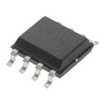
| 供应商器件封装 | 8-SO |
| 其它名称 | 497-4676-6 |
| 其它有关文件 | http://www.st.com/web/catalog/sense_power/FM142/CL1501/SC907/SS1645/LN1617/PF90931?referrer=70071840http://www.st.com/web/catalog/sense_power/FM142/CL1501/SC907/PF90931?referrer=70071840 |
| 包装 | Digi-Reel® |
| 商标 | STMicroelectronics |
| 安装类型 | 表面贴装 |
| 安装风格 | SMD/SMT |
| 封装 | Reel |
| 封装/外壳 | 8-SOIC(0.154",3.90mm 宽) |
| 封装/箱体 | SO-8 |
| 工作温度 | -40°C ~ 125°C |
| 工厂包装数量 | 2500 |
| 延迟时间 | 2µs |
| 最大功率耗散 | 500 mW |
| 最大工作温度 | + 125 C |
| 最小工作温度 | - 40 C |
| 标准包装 | 1 |
| 激励器数量 | 1 Driver |
| 电压-电源 | 12 V ~ 26 V |
| 电流-峰值 | 750mA |
| 电源电压-最小 | 12 V |
| 电源电流 | 2.5 mA |
| 类型 | Advanced Gate Driver for IGBT and Power Mosfet |
| 系列 | TD352 |
| 输入类型 | 非反相 |
| 输出数 | 1 |
| 输出端数量 | 1 |
| 配置 | Inverting |
| 配置数 | 1 |
| 高压侧电压-最大值(自举) | - |


- 商务部:美国ITC正式对集成电路等产品启动337调查
- 曝三星4nm工艺存在良率问题 高通将骁龙8 Gen1或转产台积电
- 太阳诱电将投资9.5亿元在常州建新厂生产MLCC 预计2023年完工
- 英特尔发布欧洲新工厂建设计划 深化IDM 2.0 战略
- 台积电先进制程称霸业界 有大客户加持明年业绩稳了
- 达到5530亿美元!SIA预计今年全球半导体销售额将创下新高
- 英特尔拟将自动驾驶子公司Mobileye上市 估值或超500亿美元
- 三星加码芯片和SET,合并消费电子和移动部门,撤换高东真等 CEO
- 三星电子宣布重大人事变动 还合并消费电子和移动部门
- 海关总署:前11个月进口集成电路产品价值2.52万亿元 增长14.8%


PDF Datasheet 数据手册内容提取
TD352 Advanced IGBT/MOSFET driver Features ■ 1.7 A sink / 1.3 A source (typ) current capability ■ Active Miller clamp feature ■ Desaturation detection ■ Adjustable turn-on delay ■ UVLO protection SO-8 ■ 2k V ESD protection Applications ■ 1200 V 3-phase inverter ■ Motor control systems ■ UPS Description This device is an advanced gate driver for IGBTs and power MOSFETs. Control and protection functions are included and allow the design of high reliability systems. The innovative active Miller clamp function eliminates the need for negative gate drive in most applications and allows the use of a simple bootstrap supply for the high side driver. The TD352 includes an adjustable turn-on delay. This feature can be used to implement reliable deadtime between high and low sides of a half bridge. An external resistor and capacitor are used to provide accurate timing. Table 1. Device summary Order codes Temperature range Package Packaging TD352ID Tube -40°C, +125°C SO-8 TD352IDT Tape and reel June 2011 Doc ID 11095 Rev 2 1/18 www.st.com 18
Contents TD352 Contents 1 Block diagram . . . . . . . . . . . . . . . . . . . . . . . . . . . . . . . . . . . . . . . . . . . . . . 3 2 Pin connections . . . . . . . . . . . . . . . . . . . . . . . . . . . . . . . . . . . . . . . . . . . . . 4 3 Absolute maximum ratings . . . . . . . . . . . . . . . . . . . . . . . . . . . . . . . . . . . 5 4 Electrical characteristics . . . . . . . . . . . . . . . . . . . . . . . . . . . . . . . . . . . . . 6 5 Functional description . . . . . . . . . . . . . . . . . . . . . . . . . . . . . . . . . . . . . . . 8 5.1 Input stage . . . . . . . . . . . . . . . . . . . . . . . . . . . . . . . . . . . . . . . . . . . . . . . . 8 5.2 Voltage reference . . . . . . . . . . . . . . . . . . . . . . . . . . . . . . . . . . . . . . . . . . . 8 5.3 Active Miller clamp . . . . . . . . . . . . . . . . . . . . . . . . . . . . . . . . . . . . . . . . . . 8 5.4 Turn-on delay . . . . . . . . . . . . . . . . . . . . . . . . . . . . . . . . . . . . . . . . . . . . . . . 8 5.5 Desaturation protection . . . . . . . . . . . . . . . . . . . . . . . . . . . . . . . . . . . . . . . 9 5.6 Output stage . . . . . . . . . . . . . . . . . . . . . . . . . . . . . . . . . . . . . . . . . . . . . . . 9 5.7 Undervoltage protection . . . . . . . . . . . . . . . . . . . . . . . . . . . . . . . . . . . . . . 9 6 Timing diagrams . . . . . . . . . . . . . . . . . . . . . . . . . . . . . . . . . . . . . . . . . . . 11 7 Typical performance curves . . . . . . . . . . . . . . . . . . . . . . . . . . . . . . . . . . 13 8 Application diagrams . . . . . . . . . . . . . . . . . . . . . . . . . . . . . . . . . . . . . . . 15 9 Package mechanical data . . . . . . . . . . . . . . . . . . . . . . . . . . . . . . . . . . . 16 10 Revision history . . . . . . . . . . . . . . . . . . . . . . . . . . . . . . . . . . . . . . . . . . . 17 2/18 Doc ID 11095 Rev 2
TD352 Block diagram 1 Block diagram Figure 1. TD352 block diagram (cid:17)(cid:22)(cid:54) (cid:56)(cid:42) (cid:20)(cid:14)(cid:23)(cid:75) (cid:53)(cid:54)(cid:44)(cid:47) (cid:41)(cid:46) (cid:54)(cid:40) (cid:75) (cid:54)(cid:50)(cid:37)(cid:38) (cid:67) (cid:47)(cid:53)(cid:52) (cid:54)(cid:82)(cid:69)(cid:70) (cid:79) (cid:34)(cid:76) (cid:35)(cid:36) (cid:79)(cid:76) (cid:54)(cid:44) (cid:36)(cid:69)(cid:76)(cid:65)(cid:89) (cid:82) (cid:78)(cid:84) (cid:79) (cid:36)(cid:37)(cid:51)(cid:33)(cid:52) (cid:35) (cid:35)(cid:44)(cid:33)(cid:45)(cid:48) (cid:36)(cid:69)(cid:83)(cid:65)(cid:84) (cid:52)(cid:36)(cid:19)(cid:21)(cid:18) (cid:33)(cid:45)(cid:16)(cid:18)(cid:24)(cid:18)(cid:22)(cid:86)(cid:17) Doc ID 11095 Rev 2 3/18
Pin connections TD352 2 Pin connections Figure 2. Pin connections (top view) (cid:44)(cid:49) (cid:20) (cid:27) (cid:57)(cid:43) (cid:57)(cid:53)(cid:40)(cid:41) (cid:21) (cid:26) (cid:50)(cid:56)(cid:55) (cid:55)(cid:39)(cid:22)(cid:24)(cid:21) (cid:38)(cid:39) (cid:22) (cid:25) (cid:57)(cid:47) (cid:39)(cid:40)(cid:54)(cid:36)(cid:55) (cid:23) (cid:24) (cid:38)(cid:47)(cid:36)(cid:48)(cid:51) (cid:33)(cid:45)(cid:16)(cid:18)(cid:24)(cid:18)(cid:21)(cid:86)(cid:17) T able 2. Pin description Pin n° Name Type Function IN 1 Analog input Input VREF 2 Analog output +5 V reference voltage CD 3 Timing capacitor Turn on delay DESAT 4 Analog input Desaturation protection CLAMP 5 Analog output Miller clamp VL 6 Power supply Signal ground OUT 7 Analog output Gate drive output VH 8 Power supply Positive supply 4/18 Doc ID 11095 Rev 2
TD352 Absolute maximum ratings 3 Absolute maximum ratings Table 3. A bsolute maximum ratings Symbol Parameter Value Unit VHL Maximum supply voltage (VH - VL) 28 V V Voltage on OUT, CLAMP, DESAT pins VL-0.3 to VH+0.3 V out V Voltage on other pins (IN, CD, VREF) -0.3 to 7 V other P Power dissipation 500 mW d T Storage temperature -55 to 150 °C stg T Maximum junction temperature 150 °C j R Thermal resistance junction-ambient 150 °C/W thJA ESD Electrostatic discharge (HBM) 2 kV Table 4. O perating conditions Symbol Parameter Value Unit VH Positive supply voltage vs. VL UVLO to 26 V T Operating free air temperature range -40 to 125 °C oper Doc ID 11095 Rev 2 5/18
Electrical characteristics TD352 4 Electrical characteristics T = -20 to 125 °C, VH= 16 V, unless otherwise specified. A Table 5. E lectrical characteristics Symbol Parameter Test condition Min Typ Max Unit Input V IN turn-on threshold voltage 0.8 1.0 V ton V IN turn-off threshold voltage 4.0 4.2 V toff I IN input current IN input voltage < 4.5V 1 µA inp Voltage reference (1) V Voltage reference T = 25°C 4.85 5.00 5.15 V ref I Maximum output current 10 mA ref Clamp V CLAMP pin voltage threshold 2.0 V tclamp V Clamp low voltage I = 500mA 2.5 V CL csink Delay V Voltage threshold 2.5 V tdel R Discharge resistor I=1mA 500 Ω del Desaturation protection V Desaturation threshold VH-2 V des I Source current 250 µA des Output I Output sink current V = 6V 1000 1700 mA sink out I Output source current V = VH-6V 750 1300 mA src out V Output low voltage 1 I = 20mA 0.35 V OL1 osink V Output low voltage 2 I = 500mA 2.5 V OL2 osink V Output high voltage 1 I = 20mA VH-2.5 V OH1 osource V Output high voltage 2 I = 500mA VH-4.0 V OH2 osource t Rise time C = 1nF, 10% to 90% 100 ns r L t Fall time C = 1nF, 90% to 10% 100 ns f L 10% OUT change: t Turn on propagation delay R = 4.7kΩ, no C 500 ns don d d R = 11kΩ, C = 220 pF 1.8 2.0 2.2 µs d d t Turn off propagation delay 10% OUT change 400 ns doff 6/18 Doc ID 11095 Rev 2
TD352 Electrical characteristics Table 5. Electrical characteristics (continued) Symbol Parameter Test condition Min Typ Max Unit Under voltage lockout (UVLO) UVLOH UVLO top threshold 10 11 12 V UVLOL UVLO bottom threshold 9 10 11 V V UVLO hysteresis UVLOH-UVLOL 0.5 1 V hyst Supply current I Quiescent current OUT = 0V; no load 2.5 mA in 1. Recommended capacitor range on VREF pin is 10 nF to 100 nF Doc ID 11095 Rev 2 7/18
Functional description TD352 5 Functional description 5.1 Input stage The TD352 IN input is internally clamped at about 5 V to 7 V. The input is triggered by the signal edge. When using an open collector optocoupler, the resistive pull-up resistor can be connected to either VREF or VH. Recommended pull-up resistor value with VH=16 V is from 4.7 kΩ to 22 kΩ. 5.2 Voltage reference A voltage reference is used to create accurate timing for the turn-on delay with external resistor and capacitor. A decoupling capacitor (10 nF to 100 nF) on the VREF pin is required to ensure good noise rejection. 5.3 Active Miller clamp The TD352 offers an alternative solution to the problem of Miller current in IGBT switching applications. Instead of driving the IGBT gate to a negative voltage to increase the safety margin, the TD352 uses a dedicated CLAMP pin to control the Miller current. When the IGBT is off, a low impedance path is established between the IGBT gate and emitter to carry the Miller current, and the voltage spike on the IGBT gate is greatly reduced. During turn-off, the gate voltage is monitored and the clamp output is activated when the gate voltage goes below 2 V (relative to VL). The clamp voltage is VL+4V max for a Miller current up to 500 mA. The clamp is disabled when the IN input is triggered again. The CLAMP function does not affect the turn-off characteristic, but only keeps the gate at low level throughout the off time. The main benefit is that negative voltage can be avoided in many cases, allowing a bootstrap technique for the high side driver supply. 5.4 Turn-on delay Turn-on (T ) delay is programmable through external resistor R and capacitor C for a d d accurate timing. T is approximately given by (see Figure5): a T (µs) = 0.7 * R (kΩ) * C (nF) a d d The turn-on delay can be disabled by connecting the CD pin to VREF with a 4.7 kΩ resistor. Input signals with ON-time smaller than T are ignored. a 8/18 Doc ID 11095 Rev 2
TD352 Functional description 5.5 Desaturation protection Desaturation protection ensures the protection of the IGBT in the event of overcurrent. When the DESAT voltage goes higher than VH-2V, the TD352 OUT pin is driven low. The fault state is only exited after a power-down and power-up cycle. A programmable blanking time is used to allow enough time for IGBT saturation. Blanking time is provided by an internal current source and external C capacitor. The T des bdes blanking time value is given by: T = V * C / I bdes des des des At VH=16V, T is approximately given by: bdes T (µs) = 0.056 * C (pF) bdes des 5.6 Output stage The output stage is able to sink/source 1.7 A/1.3 A (typical) at 25 °C and 1.0 A/0.75 A min. over the full temperature range. This current capability is specified near the usual IGBT Miller plateau. 5.7 Undervoltage protection Undervoltage detection protects the application in the event of a low VH supply voltage (during startup or a fault situation). During undervoltage, the OUT pin is driven low (active pull-down for VH>2V, and passive pull-down for VH<2V). Figure 3. Undervoltage protection (cid:53)(cid:54)(cid:44)(cid:47)(cid:40) (cid:53)(cid:54)(cid:44)(cid:47)(cid:44) (cid:54)(cid:67)(cid:67)(cid:77)(cid:73)(cid:78) (cid:54)(cid:40) (cid:18)(cid:54) (cid:47)(cid:53)(cid:52) (cid:38)(cid:33)(cid:53)(cid:44)(cid:52) (cid:34)(cid:46)(cid:17)(cid:19)(cid:25)(cid:19)(cid:24)(cid:87)(cid:18) Doc ID 11095 Rev 2 9/18
Functional description TD352 Figure 4. Detailed internal schematic (cid:53)(cid:54)(cid:44)(cid:47) (cid:37)(cid:81)(cid:79)(cid:82)(cid:65)(cid:43)(cid:80)(cid:82)(cid:87)(cid:86) (cid:41)(cid:46) (cid:25)(cid:56) (cid:17)(cid:54)(cid:13)(cid:20)(cid:54) (cid:54)(cid:50)(cid:37)(cid:38) (cid:21)(cid:54)(cid:0)(cid:54)(cid:82)(cid:69)(cid:70) (cid:37)(cid:81)(cid:79)(cid:82)(cid:65)(cid:38)(cid:71)(cid:78)(cid:67)(cid:91)(cid:49)(cid:72)(cid:72) (cid:35)(cid:79)(cid:78)(cid:84)(cid:82)(cid:79)(cid:76)(cid:0)(cid:34)(cid:76)(cid:79)(cid:67)(cid:75) (cid:35)(cid:36) (cid:18)(cid:14)(cid:21)(cid:54) (cid:53)(cid:20) (cid:54)(cid:40) (cid:20)(cid:23)(cid:18)(cid:87)(cid:35) (cid:37)(cid:81)(cid:79)(cid:82)(cid:65)(cid:37)(cid:78)(cid:67)(cid:79)(cid:82) (cid:37)(cid:81)(cid:79)(cid:82)(cid:65)(cid:38)(cid:71)(cid:85)(cid:67)(cid:86) (cid:35)(cid:44)(cid:33)(cid:45)(cid:48) (cid:36)(cid:37)(cid:51)(cid:33)(cid:52) (cid:18)(cid:54) (cid:54)(cid:40)(cid:13)(cid:18)(cid:54) (cid:53)(cid:19) (cid:54)(cid:40) (cid:47)(cid:53)(cid:52) (cid:54)(cid:44) (cid:34)(cid:46)(cid:17)(cid:19)(cid:25)(cid:19)(cid:25)(cid:87)(cid:18) 10/18 Doc ID 11095 Rev 2
TD352 Timing diagrams 6 Timing diagrams Figure 5. General turn-on and turn-off sequence (cid:52)(cid:87)(cid:73)(cid:78) (cid:41)(cid:46) (cid:35)(cid:36) (cid:52)(cid:65) (cid:54)(cid:40)(cid:0)(cid:76)(cid:69)(cid:86)(cid:69)(cid:76) (cid:47)(cid:53)(cid:52) (cid:52)(cid:87)(cid:79)(cid:85)(cid:84) (cid:54)(cid:44)(cid:0)(cid:76)(cid:69)(cid:86)(cid:69)(cid:76) (cid:47)(cid:80)(cid:69)(cid:78) (cid:35)(cid:44)(cid:33)(cid:45)(cid:48) (cid:54)(cid:40)(cid:0)(cid:76)(cid:69)(cid:86)(cid:69)(cid:76) (cid:45)(cid:73)(cid:76)(cid:76)(cid:69)(cid:82)(cid:0)(cid:80)(cid:76)(cid:65)(cid:84)(cid:69)(cid:65)(cid:85) (cid:54)(cid:71)(cid:69) (cid:35)(cid:76)(cid:65)(cid:77)(cid:80)(cid:0)(cid:84)(cid:72)(cid:82)(cid:69)(cid:83)(cid:72)(cid:79)(cid:76)(cid:68) (cid:54)(cid:44)(cid:0)(cid:76)(cid:69)(cid:86)(cid:69)(cid:76) (cid:54)(cid:67)(cid:69) (cid:33)(cid:45)(cid:16)(cid:18)(cid:24)(cid:18)(cid:25)(cid:86)(cid:17) Figure 6. Input and output waveform dynamic parameters (cid:52)(cid:87)(cid:73)(cid:78) (cid:54)(cid:84)(cid:79)(cid:70)(cid:70) (cid:41)(cid:46) (cid:8)(cid:76)(cid:69)(cid:86)(cid:69)(cid:76)(cid:0)(cid:77)(cid:79)(cid:68)(cid:69)(cid:9) (cid:54)(cid:84)(cid:79)(cid:78) (cid:41)(cid:46) (cid:8)(cid:69)(cid:68)(cid:71)(cid:69)(cid:0)(cid:77)(cid:79)(cid:68)(cid:69)(cid:9) (cid:54)(cid:84)(cid:79)(cid:70)(cid:70) (cid:54)(cid:84)(cid:79)(cid:78) (cid:54)(cid:40)(cid:0)(cid:76)(cid:69)(cid:86)(cid:69)(cid:76) (cid:84)(cid:68)(cid:79)(cid:70)(cid:70) (cid:47)(cid:53)(cid:52) (cid:54)(cid:44)(cid:0)(cid:76)(cid:69)(cid:86)(cid:69)(cid:76) (cid:52)(cid:87)(cid:79)(cid:85)(cid:84) (cid:84)(cid:68)(cid:79)(cid:78) (cid:33)(cid:45)(cid:16)(cid:18)(cid:24)(cid:19)(cid:16)(cid:86)(cid:17) Doc ID 11095 Rev 2 11/18
Timing diagrams TD352 Figure 7. Desaturation fault (cid:41)(cid:46) (cid:18)(cid:14)(cid:21)(cid:54) (cid:35)(cid:36) (cid:52)(cid:65) (cid:54)(cid:40)(cid:0)(cid:76)(cid:69)(cid:86)(cid:69)(cid:76) (cid:47)(cid:53)(cid:52) (cid:54)(cid:44)(cid:0)(cid:76)(cid:69)(cid:86)(cid:69)(cid:76) (cid:54)(cid:40)(cid:13)(cid:18)(cid:54) (cid:36)(cid:37)(cid:51)(cid:33)(cid:52) (cid:36)(cid:69)(cid:83)(cid:65)(cid:84)(cid:0)(cid:34)(cid:76)(cid:65)(cid:78)(cid:75)(cid:73)(cid:78)(cid:71)(cid:0)(cid:52)(cid:73)(cid:77)(cid:69) (cid:33)(cid:45)(cid:16)(cid:18)(cid:24)(cid:19)(cid:17)(cid:86)(cid:17) 12/18 Doc ID 11095 Rev 2
TD352 Typical performance curves 7 Typical performance curves Figure 8. Q uiescent current vs temperature Figure 9. Rdel resistance vs temperature (cid:18)(cid:14)(cid:21) (cid:21)(cid:16)(cid:16) (cid:18)(cid:14)(cid:16) (cid:20)(cid:16)(cid:16) (cid:86)(cid:12) (cid:36)(cid:12)(cid:17)(cid:14)(cid:21) (cid:75)(cid:80) (cid:19)(cid:16)(cid:16) (cid:80) (cid:50) (cid:44)(cid:81)(cid:3)(cid:11)(cid:17)(cid:14)(cid:16) (cid:71)(cid:72)(cid:79)(cid:3)(cid:11) (cid:18)(cid:16)(cid:16) (cid:53) (cid:16)(cid:14)(cid:21) (cid:17)(cid:16)(cid:16) (cid:16)(cid:14)(cid:16) (cid:16) (cid:13)(cid:21)(cid:16) (cid:13)(cid:18)(cid:21) (cid:16) (cid:18)(cid:21) (cid:21)(cid:16) (cid:23)(cid:21) (cid:17)(cid:16)(cid:16) (cid:17)(cid:18)(cid:21) (cid:13)(cid:21)(cid:16) (cid:13)(cid:18)(cid:21) (cid:16) (cid:18)(cid:21) (cid:21)(cid:16) (cid:23)(cid:21) (cid:17)(cid:16)(cid:16) (cid:17)(cid:18)(cid:21) (cid:55)(cid:72)(cid:80)(cid:83)(cid:3)(cid:11)(cid:131)(cid:38)(cid:12) (cid:55)(cid:72)(cid:80)(cid:83)(cid:3)(cid:11)(cid:131)(cid:38)(cid:12) (cid:33)(cid:45)(cid:16)(cid:18)(cid:24)(cid:19)(cid:18)(cid:86)(cid:17) (cid:33)(cid:45)(cid:16)(cid:18)(cid:24)(cid:19)(cid:19)(cid:86)(cid:17) Figure 10. Low level output voltage vs temp. Figure 11. High level output voltage vs temp. (cid:20)(cid:20)(cid:14)(cid:14)(cid:16)(cid:16) (cid:19)(cid:19)(cid:14)(cid:14)(cid:16)(cid:16) (cid:19)(cid:19)(cid:14)(cid:14)(cid:16)(cid:16) (cid:50)(cid:47)(cid:16)(cid:57)(cid:47)(cid:3)(cid:11)(cid:57)(cid:12)(cid:50)(cid:47)(cid:16)(cid:57)(cid:47)(cid:3)(cid:11)(cid:57)(cid:12) (cid:18)(cid:18)(cid:14)(cid:14)(cid:16)(cid:16) (cid:41)(cid:41)(cid:79)(cid:79)(cid:83)(cid:83)(cid:73)(cid:73)(cid:78)(cid:78)(cid:75)(cid:75)(cid:29)(cid:29)(cid:21)(cid:21)(cid:16)(cid:16)(cid:16)(cid:16)(cid:77)(cid:77)(cid:33)(cid:33) (cid:43)(cid:16)(cid:57)(cid:50)(cid:43)(cid:3)(cid:11)(cid:57)(cid:12)(cid:43)(cid:16)(cid:57)(cid:50)(cid:43)(cid:3)(cid:11)(cid:57)(cid:12) (cid:18)(cid:18)(cid:14)(cid:14)(cid:16)(cid:16) (cid:41)(cid:41)(cid:79)(cid:79)(cid:83)(cid:83)(cid:79)(cid:79)(cid:85)(cid:85)(cid:82)(cid:82)(cid:67)(cid:67)(cid:69)(cid:69)(cid:29)(cid:29)(cid:21)(cid:21)(cid:16)(cid:16)(cid:16)(cid:16)(cid:77)(cid:77)(cid:33)(cid:33) (cid:57)(cid:57) (cid:17)(cid:17)(cid:14)(cid:14)(cid:16)(cid:16) (cid:57)(cid:57) (cid:17)(cid:17)(cid:14)(cid:14)(cid:16)(cid:16) (cid:41)(cid:41)(cid:79)(cid:79)(cid:83)(cid:83)(cid:79)(cid:79)(cid:85)(cid:85)(cid:82)(cid:82)(cid:67)(cid:67)(cid:69)(cid:69)(cid:29)(cid:29)(cid:18)(cid:18)(cid:16)(cid:16)(cid:77)(cid:77)(cid:33)(cid:33) (cid:41)(cid:41)(cid:79)(cid:79)(cid:83)(cid:83)(cid:73)(cid:73)(cid:78)(cid:78)(cid:75)(cid:75)(cid:29)(cid:29)(cid:18)(cid:18)(cid:16)(cid:16)(cid:77)(cid:77)(cid:33)(cid:33) (cid:16)(cid:16)(cid:14)(cid:14)(cid:16)(cid:16) (cid:16)(cid:16)(cid:14)(cid:14)(cid:16)(cid:16) (cid:13)(cid:13)(cid:21)(cid:21)(cid:16)(cid:16) (cid:13)(cid:13)(cid:18)(cid:18)(cid:21)(cid:21) (cid:16)(cid:16) (cid:18)(cid:18)(cid:21)(cid:21) (cid:21)(cid:21)(cid:16)(cid:16) (cid:23)(cid:23)(cid:21)(cid:21) (cid:17)(cid:17)(cid:16)(cid:16)(cid:16)(cid:16) (cid:17)(cid:17)(cid:18)(cid:18)(cid:21)(cid:21) (cid:13)(cid:13)(cid:21)(cid:21)(cid:16)(cid:16) (cid:13)(cid:13)(cid:18)(cid:18)(cid:21)(cid:21) (cid:16)(cid:16) (cid:18)(cid:18)(cid:21)(cid:21) (cid:21)(cid:21)(cid:16)(cid:16) (cid:23)(cid:23)(cid:21)(cid:21) (cid:17)(cid:17)(cid:16)(cid:16)(cid:16)(cid:16) (cid:17)(cid:17)(cid:18)(cid:18)(cid:21)(cid:21) (cid:55)(cid:55)(cid:72)(cid:72)(cid:80)(cid:80)(cid:83)(cid:83)(cid:3)(cid:3)(cid:11)(cid:11)(cid:131)(cid:131)(cid:38)(cid:38)(cid:12)(cid:12) (cid:55)(cid:55)(cid:72)(cid:72)(cid:80)(cid:80)(cid:83)(cid:83)(cid:3)(cid:3)(cid:11)(cid:11)(cid:131)(cid:131)(cid:38)(cid:38)(cid:12)(cid:12) (cid:33)(cid:45)(cid:16)(cid:18)(cid:24)(cid:19)(cid:20)(cid:86)(cid:17) (cid:33)(cid:45)(cid:16)(cid:18)(cid:24)(cid:19)(cid:21)(cid:86)(cid:17) Doc ID 11095 Rev 2 13/18
Typical performance curves TD352 Figure 12. Sink current vs temperature Figure 13. Source current vs temperature (cid:18)(cid:16)(cid:16)(cid:16) (cid:17)(cid:22)(cid:16)(cid:16) (cid:17)(cid:24)(cid:16)(cid:16) (cid:17)(cid:20)(cid:16)(cid:16) (cid:36)(cid:12) (cid:17)(cid:22)(cid:16)(cid:16) (cid:36)(cid:12) (cid:80) (cid:80) (cid:44)(cid:86)(cid:76)(cid:81)(cid:78)(cid:3)(cid:11) (cid:17)(cid:20)(cid:16)(cid:16) (cid:44)(cid:86)(cid:85)(cid:70)(cid:3)(cid:11) (cid:17)(cid:18)(cid:16)(cid:16) (cid:17)(cid:16)(cid:16)(cid:16) (cid:17)(cid:18)(cid:16)(cid:16) (cid:17)(cid:16)(cid:16)(cid:16) (cid:24)(cid:16)(cid:16) (cid:13)(cid:21)(cid:16) (cid:13)(cid:18)(cid:21) (cid:16) (cid:18)(cid:21) (cid:21)(cid:16) (cid:23)(cid:21) (cid:17)(cid:16)(cid:16) (cid:17)(cid:18)(cid:21) (cid:13)(cid:21)(cid:16) (cid:13)(cid:18)(cid:21) (cid:16) (cid:18)(cid:21) (cid:21)(cid:16) (cid:23)(cid:21) (cid:17)(cid:16)(cid:16) (cid:17)(cid:18)(cid:21) (cid:55)(cid:72)(cid:80)(cid:83)(cid:3)(cid:11)(cid:131)(cid:38)(cid:12) (cid:55)(cid:72)(cid:80)(cid:83)(cid:3)(cid:11)(cid:131)(cid:38)(cid:12) (cid:33)(cid:45)(cid:16)(cid:18)(cid:24)(cid:19)(cid:22)(cid:86)(cid:17) (cid:33)(cid:45)(cid:16)(cid:18)(cid:24)(cid:19)(cid:23)(cid:86)(cid:17) 14/18 Doc ID 11095 Rev 2
TD352 Application diagrams 8 Application diagrams Figure 14. Single supply IGBT drive with active Miller clamp and DESAT protection (cid:17)(cid:22)(cid:54) (cid:56)(cid:42) (cid:20)(cid:14)(cid:23)(cid:75) (cid:53)(cid:54)(cid:44)(cid:47) (cid:41)(cid:46) (cid:54)(cid:40) (cid:75) (cid:54)(cid:50)(cid:37)(cid:38) (cid:67) (cid:47)(cid:53)(cid:52) (cid:54)(cid:82)(cid:69)(cid:70) (cid:79) (cid:34)(cid:76) (cid:35)(cid:36) (cid:79)(cid:76) (cid:54)(cid:44) (cid:36)(cid:69)(cid:76)(cid:65)(cid:89) (cid:78)(cid:84)(cid:82) (cid:79) (cid:36)(cid:37)(cid:51)(cid:33)(cid:52) (cid:35) (cid:35)(cid:44)(cid:33)(cid:45)(cid:48) (cid:36)(cid:69)(cid:83)(cid:65)(cid:84) (cid:52)(cid:36)(cid:19)(cid:21)(cid:18) (cid:33)(cid:45)(cid:16)(cid:18)(cid:24)(cid:19)(cid:24)(cid:86)(cid:17) Figure 15. Use of DESAT input for direct overcurrent detection (cid:17)(cid:22)(cid:54) (cid:56)(cid:42) (cid:20)(cid:14)(cid:23)(cid:75) (cid:53)(cid:54)(cid:44)(cid:47) (cid:41)(cid:46) (cid:54)(cid:40) (cid:75) (cid:54)(cid:82)(cid:69)(cid:70) (cid:54)(cid:50)(cid:37)(cid:38) (cid:54)(cid:82)(cid:69)(cid:70) (cid:79)(cid:67) (cid:47)(cid:53)(cid:52) (cid:34)(cid:76) (cid:35)(cid:36) (cid:79)(cid:76) (cid:54)(cid:44) (cid:36)(cid:69)(cid:76)(cid:65)(cid:89) (cid:78)(cid:84)(cid:82) (cid:79) (cid:36)(cid:37)(cid:51)(cid:33)(cid:52) (cid:35) (cid:35)(cid:44)(cid:33)(cid:45)(cid:48) (cid:36)(cid:69)(cid:83)(cid:65)(cid:84) (cid:52)(cid:36)(cid:19)(cid:21)(cid:18) (cid:33)(cid:45)(cid:16)(cid:18)(cid:24)(cid:19)(cid:25)(cid:86)(cid:17) Figure 16. Large IGBT drive with negative voltage gate drive and optional current buffers (cid:56)(cid:42) (cid:20)(cid:14)(cid:23)(cid:75) (cid:53)(cid:54)(cid:44)(cid:47) (cid:41)(cid:46) (cid:54)(cid:40) (cid:47)(cid:80)(cid:84)(cid:73)(cid:79)(cid:78)(cid:65)(cid:76) (cid:17)(cid:22)(cid:54) (cid:75) (cid:54)(cid:50)(cid:37)(cid:38) (cid:67) (cid:47)(cid:53)(cid:52) (cid:54)(cid:82)(cid:69)(cid:70) (cid:79) (cid:34)(cid:76) (cid:13)(cid:17)(cid:16)(cid:54) (cid:35)(cid:36) (cid:36)(cid:69)(cid:76)(cid:65)(cid:89) (cid:78)(cid:84)(cid:82)(cid:79)(cid:76) (cid:54)(cid:44) (cid:79) (cid:36)(cid:37)(cid:51)(cid:33)(cid:52) (cid:35) (cid:35)(cid:44)(cid:33)(cid:45)(cid:48) (cid:36)(cid:69)(cid:83)(cid:65)(cid:84) (cid:52)(cid:36)(cid:19)(cid:21)(cid:18) (cid:47)(cid:80)(cid:84)(cid:73)(cid:79)(cid:78)(cid:65)(cid:76) (cid:33)(cid:45)(cid:16)(cid:18)(cid:24)(cid:20)(cid:16)(cid:86)(cid:17) Doc ID 11095 Rev 2 15/18
Package mechanical data TD352 9 Package mechanical data In order to meet environmental requirements, ST offers these devices in different grades of ECOPACK® packages, depending on their level of environmental compliance. ECOPACK® specifications, grade definitions and product status are available at: www.st.com. ECOPACK® is an ST trademark. T able 6. SO-8 mechanical data mm. inch Dim. Min. Typ Max. Min. Typ. Max. A 1.35 1.75 0.053 0.069 A1 0.10 0.25 0.04 0.010 A2 1.10 1.65 0.043 0.065 B 0.33 0.51 0.013 0.020 C 0.19 0.25 0.007 0.010 D 4.80 5.00 0.189 0.197 E 3.80 4.00 0.150 0.157 e 1.27 0.050 H 5.80 6.20 0.228 0.244 h 0.25 0.50 0.010 0.020 L 0.40 1.27 0.016 0.050 k (max.) 8 ddd 0.1 0.04 Figure 17. SO-8 mechanical drawing (cid:16)(cid:16)(cid:17)(cid:22)(cid:16)(cid:18)(cid:19)(cid:15)(cid:35) 16/18 Doc ID 11095 Rev 2
TD352 Revision history 10 Revision history T able 7. Document revision history Date Revision Changes 01-Nov-2004 1 Initial release Deleted order code TD352IN. 13-Jun-2011 2 Content reworked to improve readability. Doc ID 11095 Rev 2 17/18
TD352 Please Read Carefully: Information in this document is provided solely in connection with ST products. STMicroelectronics NV and its subsidiaries (“ST”) reserve the right to make changes, corrections, modifications or improvements, to this document, and the products and services described herein at any time, without notice. All ST products are sold pursuant to ST’s terms and conditions of sale. Purchasers are solely responsible for the choice, selection and use of the ST products and services described herein, and ST assumes no liability whatsoever relating to the choice, selection or use of the ST products and services described herein. No license, express or implied, by estoppel or otherwise, to any intellectual property rights is granted under this document. If any part of this document refers to any third party products or services it shall not be deemed a license grant by ST for the use of such third party products or services, or any intellectual property contained therein or considered as a warranty covering the use in any manner whatsoever of such third party products or services or any intellectual property contained therein. UNLESS OTHERWISE SET FORTH IN ST’S TERMS AND CONDITIONS OF SALE ST DISCLAIMS ANY EXPRESS OR IMPLIED WARRANTY WITH RESPECT TO THE USE AND/OR SALE OF ST PRODUCTS INCLUDING WITHOUT LIMITATION IMPLIED WARRANTIES OF MERCHANTABILITY, FITNESS FOR A PARTICULAR PURPOSE (AND THEIR EQUIVALENTS UNDER THE LAWS OF ANY JURISDICTION), OR INFRINGEMENT OF ANY PATENT, COPYRIGHT OR OTHER INTELLECTUAL PROPERTY RIGHT. UNLESS EXPRESSLY APPROVED IN WRITING BY AN AUTHORIZED ST REPRESENTATIVE, ST PRODUCTS ARE NOT RECOMMENDED, AUTHORIZED OR WARRANTED FOR USE IN MILITARY, AIR CRAFT, SPACE, LIFE SAVING, OR LIFE SUSTAINING APPLICATIONS, NOR IN PRODUCTS OR SYSTEMS WHERE FAILURE OR MALFUNCTION MAY RESULT IN PERSONAL INJURY, DEATH, OR SEVERE PROPERTY OR ENVIRONMENTAL DAMAGE. ST PRODUCTS WHICH ARE NOT SPECIFIED AS "AUTOMOTIVE GRADE" MAY ONLY BE USED IN AUTOMOTIVE APPLICATIONS AT USER’S OWN RISK. Resale of ST products with provisions different from the statements and/or technical features set forth in this document shall immediately void any warranty granted by ST for the ST product or service described herein and shall not create or extend in any manner whatsoever, any liability of ST. ST and the ST logo are trademarks or registered trademarks of ST in various countries. Information in this document supersedes and replaces all information previously supplied. The ST logo is a registered trademark of STMicroelectronics. All other names are the property of their respective owners. © 2011 STMicroelectronics - All rights reserved STMicroelectronics group of companies Australia - Belgium - Brazil - Canada - China - Czech Republic - Finland - France - Germany - Hong Kong - India - Israel - Italy - Japan - Malaysia - Malta - Morocco - Philippines - Singapore - Spain - Sweden - Switzerland - United Kingdom - United States of America www.st.com 18/18 Doc ID 11095 Rev 2