ICGOO在线商城 > 集成电路(IC) > PMIC - 栅极驱动器 > MCP1401T-E/OT

 Datasheet下载
- 型号: MCP1401T-E/OT
- 制造商: Microchip
- 库位|库存: xxxx|xxxx
- 要求:
| 数量阶梯 | 香港交货 | 国内含税 |
| +xxxx | $xxxx | ¥xxxx |
查看当月历史价格
查看今年历史价格
MCP1401T-E/OT产品简介:
ICGOO电子元器件商城为您提供MCP1401T-E/OT由Microchip设计生产,在icgoo商城现货销售,并且可以通过原厂、代理商等渠道进行代购。 MCP1401T-E/OT价格参考。MicrochipMCP1401T-E/OT封装/规格:PMIC - 栅极驱动器, Low-Side Gate Driver IC Inverting SOT-23-5。您可以下载MCP1401T-E/OT参考资料、Datasheet数据手册功能说明书,资料中有MCP1401T-E/OT 详细功能的应用电路图电压和使用方法及教程。
MCP1401T-E/OT 是 Microchip Technology 公司推出的一款 PMIC(电源管理集成电路)中的栅极驱动器产品。其主要应用场景包括以下方面:

1. 直流电机驱动:MCP1401T-E/OT 可用于驱动小型直流电机的功率 MOSFET 栅极,通过高效地控制开关速度来优化电机性能和能效。

2. LED 驱动器应用:在 LED 照明系统中,该器件可以用来驱动 MOSFET 或 IGBT,实现对 LED 电流的精确控制,从而提供稳定的亮度输出。

3. 电源转换电路:适用于 DC-DC 转换器、升压/降压电路等场景,作为开关元件的驱动器,提高转换效率并降低功耗。

4. 电池管理系统 (BMS):在电池保护和管理电路中,此栅极驱动器可用于快速响应电池过充、过放及短路保护需求,确保系统的安全运行。

5. 消费类电子产品:例如便携式设备、家用电器等需要低功耗高性能电源管理方案的产品中,MCP1401T-E/OT 提供了紧凑且可靠的解决方案。

6. 工业自动化控制:在工业领域内,这款栅极驱动器能够支持各种传感器接口、执行机构以及复杂控制系统中的功率级驱动任务。

7. 通信与网络设备:对于路由器、交换机等需要稳定供电环境下的组件来说,它同样具备良好的适应性。

总之,MCP1401T-E/OT 凭借其简单易用的设计、较小的封装尺寸以及出色的电气特性,在众多电子项目中都发挥了重要作用。
| 参数 | 数值 |
| 产品目录 | 集成电路 (IC)半导体 |
| 描述 | IC MOSFET DRVR INV 500MA SOT23-5门驱动器 0.5A Sngl MOSFET Drvr |
| 产品分类 | PMIC - MOSFET,电桥驱动器 - 外部开关集成电路 - IC |
| 品牌 | Microchip Technology |
| 产品手册 | |
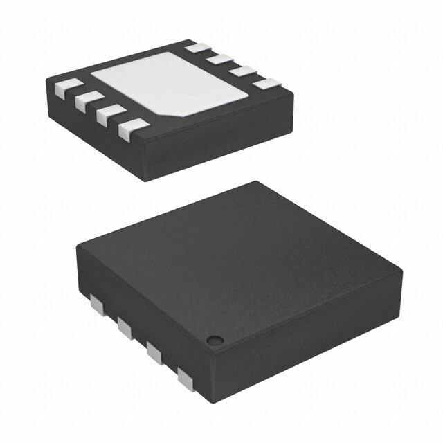
| 产品图片 |
|
| rohs | 符合RoHS无铅 / 符合限制有害物质指令(RoHS)规范要求 |
| 产品系列 | 电源管理 IC,门驱动器,Microchip Technology MCP1401T-E/OT- |
| 数据手册 | http://www.microchip.com/mymicrochip/filehandler.aspx?ddocname=en530890 |
| 产品型号 | MCP1401T-E/OT |
| PCN设计/规格 | http://www.microchip.com/mymicrochip/NotificationDetails.aspx?id=5579&print=viewhttp://www.microchip.com/mymicrochip/NotificationDetails.aspx?pcn=SYST-08VAUY636&print=view |
| 上升时间 | 19 ns |
| 下降时间 | 15 ns |
| 产品 | MOSFET Gate Drivers |
| 产品目录页面 | |
| 产品种类 | 门驱动器 |
| 供应商器件封装 | SOT-23-5 |
| 其它名称 | MCP1401T-E/OTCT |
| 包装 | 剪切带 (CT) |
| 商标 | Microchip Technology |
| 安装类型 | 表面贴装 |
| 安装风格 | SMD/SMT |
| 封装 | Reel |
| 封装/外壳 | SC-74A,SOT-753 |
| 封装/箱体 | SOT-23-5 |
| 工作温度 | -40°C ~ 125°C |
| 工厂包装数量 | 3000 |
| 延迟时间 | 35ns |
| 最大功率耗散 | 390 mW |
| 最大工作温度 | + 125 C |
| 最小工作温度 | - 40 C |
| 标准包装 | 1 |
| 激励器数量 | 1 Driver |
| 电压-电源 | 4.5 V ~ 18 V |
| 电流-峰值 | 500mA |
| 电源电压-最大 | 18 V |
| 电源电压-最小 | 4.5 V |
| 电源电流 | 0.2 mA |
| 类型 | Inverting |
| 输入类型 | 反相 |
| 输出数 | 1 |
| 输出电流 | 0.5 A |
| 输出端数量 | 1 |
| 配置 | 低端 |
| 配置数 | 1 |
| 高压侧电压-最大值(自举) | - |


- 商务部:美国ITC正式对集成电路等产品启动337调查
- 曝三星4nm工艺存在良率问题 高通将骁龙8 Gen1或转产台积电
- 太阳诱电将投资9.5亿元在常州建新厂生产MLCC 预计2023年完工
- 英特尔发布欧洲新工厂建设计划 深化IDM 2.0 战略
- 台积电先进制程称霸业界 有大客户加持明年业绩稳了
- 达到5530亿美元!SIA预计今年全球半导体销售额将创下新高
- 英特尔拟将自动驾驶子公司Mobileye上市 估值或超500亿美元
- 三星加码芯片和SET,合并消费电子和移动部门,撤换高东真等 CEO
- 三星电子宣布重大人事变动 还合并消费电子和移动部门
- 海关总署:前11个月进口集成电路产品价值2.52万亿元 增长14.8%


PDF Datasheet 数据手册内容提取
MCP1401/02 Tiny 500 mA, High-Speed Power MOSFET Driver Features General Description • High Peak Output Current: 500mA (typical) The MCP1401/02 are high-speed MOSFET drivers • Wide Input Supply Voltage Operating Range: capable of providing 500mA of peak current. The inverting or non-inverting single channel output is - 4.5V to 18V directly controlled from either TTL or CMOS (3V to • Low Shoot-Through/Cross-Conduction Current in 18V). These devices also feature low shoot-through Output Stage current, matched rise/fall times and propagation delays • High Capacitive Load Drive Capability: which make them ideal for high switching frequency - 470pF in 19ns (typical) applications. - 1000pF in 34ns (typical) The MCP1401/02 devices operate from a single 4.5V • Short Delay Times: 35ns (typical) to 18V power supply and can easily charge and • Matched Rise/Fall Times discharge 470pF gate capacitance in under 19ns • Low Supply Current: (typical). They provide low enough impedances in both the On and Off states to ensure the MOSFET’s - With Logic ‘1’ Input – 0.85mA (typical) intended state will not be affected, even by large - With Logic ‘0’ Input – 0.1mA (typical) transients. • Latch-Up Protected: Will Withstand 500mA These devices are highly latch-up resistant under any Reverse Current conditions within their power and voltage ratings. They • Logic Input Will Withstand Negative Swing up to 5V are not subject to damage when up to 5V of noise • Space-Saving 5-Lead SOT-23 Package spiking (of either polarity) occurs on the Ground pin. They can accept, without damage or logic upset, up to Applications 500mA of reverse current being forced back into their outputs. All terminals are fully protected against • Switch Mode Power Supplies Electrostatic Discharge (ESD) up to 1kV (HBM) and • Pulse Transformer Drive 300V (MM). • Line Drivers • Motor and Solenoid Drive Package Types SOT-23 MCP1401 MCP1402 GND 1 5 OUT OUT VDD 2 IN 3 4 GND GND 2007-2014 Microchip Technology Inc. DS20002052D-page 1
MCP1401/02 Functional Block Diagram V DD Inverting 850µA 300mV Output Non-inverting Input Effective 4.7V MCP1401 Inverting Input C=25pF MCP1402 Non-inverting (Each Input) GND DS20002052D-page 2 2007-2014 Microchip Technology Inc.
MCP1401/02 1.0 ELECTRICAL † Notice: Stresses above those listed under “Maximum CHARACTERISTICS Ratings” may cause permanent damage to the device. This is a stress rating only and functional operation of the device at those or any other conditions above those Absolute Maximum Ratings† indicated in the operational sections of this specification is not intended. Exposure to maximum Supply Voltage.....................................................+20V rating conditions for extended periods may affect Input Voltage....................(V +0.3V) to (GND–5V) DD device reliability. Input Current (V >V )...................................50mA IN DD Package Power Dissipation (T =50oC) A SOT-23-5........................................................0.39W DC CHARACTERISTICS (Note 2) Electrical Specifications: Unless otherwise indicated, T =+25°C, with 4.5VV 18V. A DD Parameters Sym. Min. Typ. Max. Units Conditions Input Logic ‘1’, High Input Voltage VIH 2.4 1.5 — V Logic ‘0’, Low Input Voltage VIL — 1.3 0.8 V Input Current I -1 — 1 µA 0VV V IN IN DD Input Voltage V -5 — V +0.3 V IN DD Output High Output Voltage V V –0.025 — — V DC Test OH DD Low Output Voltage V — — 0.025 V DC Test OL Output Resistance, High R — 12 18 I =10mA, V =18V OH OUT DD Output Resistance, Low R — 10 16 I =10mA, V =18V OL OUT DD Peak Output Current I — 0.5 — A V 18V (Note2) PK DD Latch-Up Protection I — >0.5 — A Duty cycle2%, t300µs REV Withstand Reverse Current Switching Time (Note1) Rise Time t — 19 25 ns Figure4-1, Figure4-2 R C =470pF L Fall Time t — 15 20 ns Figure4-1, Figure4-2 F C =470pF L Delay Time t — 35 40 ns Figure4-1, Figure4-2 D1 Delay Time t — 35 40 ns Figure4-1, Figure4-2 D2 Power Supply Supply Voltage V 4.5 — 18.0 V DD Power Supply Current I — 0.85 1.1 mA V =3V S IN I — 0.10 0.20 mA V =0V S IN Note 1: Switching times ensured by design. 2: Tested during characterization, not production tested. 2007-2014 Microchip Technology Inc. DS20002052D-page 3
MCP1401/02 DC CHARACTERISTICS (OVER OPERATING TEMPERATURE RANGE) Electrical Specifications: Unless otherwise indicated, operating temperature range with 4.5VV 18V. DD Parameters Sym. Min. Typ. Max. Units Conditions Input Logic ‘1’, High Input Voltage VIH 2.4 — — V Logic ‘0’, Low Input Voltage VIL — — 0.8 V Input Current I -10 — +10 µA 0VV V IN IN DD Input Voltage V -5 — V +0.3 V IN DD Output High Output Voltage V V –0.025 — — V DC TEST OH DD Low Output Voltage V — — 0.025 V DC TEST OL Output Resistance, High R — 16 18 I =10mA, V =18V OH OUT DD Output Resistance, Low R — 16 19 I =10mA, V =18V OL OUT DD Switching Time (Note1) Rise Time t — 20 30 ns Figure4-1, Figure4-2 R C =470pF L Fall Time t — 18 28 ns Figure4-1, Figure4-2 F C =470pF L Delay Time t — 40 51 ns Figure4-1, Figure4-2 D1 Delay Time t — 40 51 ns Figure4-1, Figure4-2 D2 Power Supply Supply Voltage V 4.5 — 18.0 V DD Power Supply Current I — 0.90 1.10 mA V =3V S IN — 0.11 0.20 mA V =0V IN Note 1: Switching times ensured by design. 2: Tested during characterization, not production tested. TEMPERATURE CHARACTERISTICS Electrical Specifications: Unless otherwise noted, all parameters apply with 4.5VV 18V. DD Parameters Sym. Min. Typ. Max. Units Conditions Temperature Ranges Specified Temperature Range T -40 — +125 °C A Maximum Junction Temperature T — — +150 °C J Storage Temperature Range T -65 — +150 °C A Package Thermal Resistances Thermal Resistance, 5L-SOT-23 — 220.7 — °C/W JA DS20002052D-page 4 2007-2014 Microchip Technology Inc.
MCP1401/02 2.0 TYPICAL PERFORMANCE CURVES Note: The graphs and tables provided following this note are a statistical summary based on a limited number of samples and are provided for informational purposes only. The performance characteristics listed herein are not tested or guaranteed. In some graphs or tables, the data presented may be outside the specified operating range (e.g., outside specified power supply range) and therefore outside the warranted range. Note: Unless otherwise indicated, T =+25°C with 4.5VV 18V. A DD 350 350 300 3300 pF 300 3300 pF ns) 250 ns) 250 me ( 200 me ( 200 Rise TI 110500 1000 pF 470 pF Fall Ti 110500 100 pF 470 pF 100 pF 1000 pF 50 50 0 0 4 6 8 10 12 14 16 18 4 6 8 10 12 14 16 18 Supply Voltage (V) Supply Voltage (V) FIGURE 2-1: Rise Time vs. Supply FIGURE 2-4: Fall Time vs. Supply Voltage. Voltage. 250 250 12V 12V 200 200 ns) ns) Rise Time ( 110500 18V Fall Time ( 110500 18V 50 5V 50 5V 0 0 100 1000 10000 100 1000 10000 Capacitive Load (pF) Capacitve Load (pF) FIGURE 2-2: Rise Time vs. Capacitive FIGURE 2-5: Fall Time vs. Capacitive Load. Load. 34 44 30 CVDLOD A=D 1=2 4V70 pF tRISE y (ns) 4423 tD1 VDD= 12V e (ns) 2226 tFALL n Dela 4401 m o Ti 18 gati 39 tD2 pa 38 14 o Pr 37 10 36 -40 -25 -10 5 20 35 50 65 80 95 110125 4 5 6 7 8 9 10 Temperature (oC) Input Amplitude (V) FIGURE 2-3: Rise and Fall Times vs. FIGURE 2-6: Propagation Delay vs. Input Temperature. Amplitude. 2007-2014 Microchip Technology Inc. DS20002052D-page 5
MCP1401/02 Note: Unless otherwise indicated, T =+25°C with 4.5VV 18V. A DD 80 1.2 ns) 70 mA) 1.0 Input = 1 VDD = 18V ay ( tD1 nt ( 0.8 Propagation Del 456000 tD2 Quiescent Curre 000...246 Input = 0 30 0.0 4 6 8 10 12 14 16 18 -40 -25 -10 5 20 35 50 65 80 95 110125 Supply Voltage (V) Temperature (oC) FIGURE 2-7: Propagation Delay Time vs. FIGURE 2-10: Quiescent Current vs. Supply Voltage. Temperature. 60 2.2 ay (ns) 5505 VDD = 12V tD1 d (V) 2.21 VHI el ol D h 1.9 pagation 4405 tD2 put Thres 11..78 VLO o 35 n Pr I 1.6 30 1.5 -40 -25 -10 5 20 35 50 65 80 95 110125 4 6 8 10 12 14 16 18 Temperature (oC) Supply Voltage (V) FIGURE 2-8: Propagation Delay Time vs. FIGURE 2-11: Input Threshold vs. Supply Temperature. Voltage. 1.2 2.4 nt Current (mA) 001...680 Input = 1 Threshold (V) 1222....92123 VHI VDD = 12V Quiesce 00..24 Input = 0 Input 11..78 VLO 0.0 1.6 4 6 8 10 12 14 16 18 -40 -25 -10 5 20 35 50 65 80 95 110125 Supply Voltage (V) Temperature (oC) FIGURE 2-9: Quiescent Current vs. FIGURE 2-12: Input Threshold vs. Supply Voltage. Temperature. Note: Unless otherwise indicated, T =+25°C with 4.5VV 18V. A DD DS20002052D-page 6 2007-2014 Microchip Technology Inc.
MCP1401/02 150 80 VDD = 18V 2 MHz 70 VDD = 18V 6,800 pF A) 125 A) m m 60 nt ( 100 100 kHz 1 MHz nt ( 50 3,300 pF urre 75 urre 40 100 pF pply C 50 200 kHz 50 kHz pply C 2300 470 pF 1,000 pF Su 25 Su 10 0 0 100 1000 10000 10 100 1000 Capacitive Load (pF) Frequency (kHz) FIGURE 2-13: Supply Current vs. FIGURE 2-16: Supply Current vs. Capacitive Load. Frequency. 70 50 VDD = 12V 2 MHz VDD = 12V 6,800 pF 60 ply Current (mA) 23450000 100 kHz 50 kHz 200 1k HMzHz pply Voltage (V) 234000 100 pF470 pF3,300 pF 1,000 pF up Su 10 S 10 0 0 100 1000 10000 10 100 1000 Capacitive Load (pF) Frequency (kHz) FIGURE 2-14: Supply Current vs. FIGURE 2-17: Supply Current vs. Capacitive Load. Frequency. 30 25 VDD = 6V 2 MHz VDD = 6V 6,800 pF A) 25 100 kHz 1 MHz A) 20 3,300 pF m m ent ( 20 ent ( 15 100 pF Curr 15 50 kHz 200 kHz Curr 10 470 pF ply 10 ply 1,000 pF p p Su 5 Su 5 0 0 100 1000 10000 10 100 1000 Capacitive Load (pF) Frequency (kHz) FIGURE 2-15: Supply Current vs. FIGURE 2-18: Supply Current vs. Capacitive Load. Frequency. 2007-2014 Microchip Technology Inc. DS20002052D-page 7
MCP1401/02 Note: Unless otherwise indicated, T =+25°C with 4.5VV 18V. A DD 60 V = 0V (MCP1401) IN 50 VIN= 5V (MCP1402) T = +125oC (cid:525)(cid:12) 40 J ( UT-HI 30 O R 20 T = +25oC J 10 0 4 6 8 10 12 14 16 18 Supply Voltage (V) FIGURE 2-19: Output Resistance (Output High) vs. Supply Voltage. 50 V = 5V (MCP1401) 45 IN V = 0V (MCP1402) IN 40 T = +125oC (cid:525)(cid:12) 35 J ( O 30 UT-L 25 O R 20 T = +25oC 15 J 10 5 4 6 8 10 12 14 16 18 Supply Voltage (V) FIGURE 2-20: Output Resistance (Output Low) vs. Supply Voltage. 1E-7 c) e s A* y ( 1E-8 g er n E er 1E-9 v o s s o Cr 1E-10 4 6 8 10 12 14 16 18 Supply Voltage (V) FIGURE 2-21: Crossover Energy vs. Supply Voltage. DS20002052D-page 8 2007-2014 Microchip Technology Inc.
MCP1401/02 3.0 PIN DESCRIPTIONS The description of the pins are listed in Table3-1. TABLE 3-1: PIN FUNCTION TABLE(1) Pin No. MCP1401 MCP1402 Description 1 GND GND Ground 2 V V Supply Input DD DD 3 IN IN Control Input 4 GND GND Ground 5 OUT OUT Output Note 1: Duplicate pins must be connected for proper operation. 3.1 Supply Input (V ) 3.3 Ground (GND) DD V is the bias supply input for the MOSFET driver and Ground is the Device Return pin. The Ground pin DD has a voltage range of 4.5V to 18V. This input must be should have a low-impedance connection to the bias decoupled to ground with a local capacitor. This bypass supply source return. High peak currents will flow out capacitor provides a localized low-impedance path for the Ground pin when the capacitive load is being the peak currents that are to be provided to the load. discharged. 3.2 Control Input (IN) 3.4 Output (OUT, OUT) The MOSFET driver input is a high-impedance, TTL/ The output is a CMOS push-pull output that is capable CMOS-compatible input. The input also has hysteresis of sourcing and sinking 0.5A of peak current between the high and low input levels, allowing them to (V =18V). The low output impedance ensures the DD be driven from slow rising and falling signals and to gate of the external MOSFET will stay in the intended provide noise immunity. state even during large transients. This output also has a reverse current latch-up rating of 0.5A. 2007-2014 Microchip Technology Inc. DS20002052D-page 9
MCP1401/02 4.0 APPLICATION INFORMATION V =18V DD 4.1 General Information 0.1µF 1µF Ceramic MOSFET drivers are high-speed, high-current devices which are intended to source/sink high peak currents to charge/discharge the gate capacitance of external MOSFETs or IGBTs. In high-frequency switching power supplies, the PWM controller may not have the drive Input Output capability to directly drive the power MOSFET. A C =470pF L MOSFET driver like the MCP1401/02 family can be used to provide additional source/sink current MCP1402 capability. 4.2 MOSFET Driver Timing +5V The ability of a MOSFET driver to transition from a fully- 90% off state to a fully-on state is characterized by the Input driver’s rise time (t ), fall time (t ), and propagation R F 10% delays (tD1 and tD2). The MCP1401/02 family of drivers 0V can typically charge and discharge a 470pF load 18V capacitance in 19ns, along with a typical matched tD190% tD2 90% propagation delay of 35ns. Figures4-1 and4-2 show Output tR tF the test circuit and timing waveform used to verify the 0V 10% 10% MCP1401/02 timing. FIGURE 4-2: Non-Inverting Driver Timing V =18V Waveform. DD 0.1µF 1µF Ceramic 4.3 Decoupling Capacitors Careful layout and decoupling capacitors are highly recommended when using MOSFET drivers. Large currents are required to charge and discharge capacitive loads quickly. For example, approximately Input Output 550mA are needed to charge a 470pF load with 18V C =470pF L in 15ns. MCP1401 To operate the MOSFET driver over a wide frequency range with low supply impedance, it is recommended to place a ceramic and low ESR film capacitor in parallel between the driver V and GND. A 1.0µF low ESR DD +5V film capacitor and a 0.1µF ceramic capacitor placed 90% between pins 2 and 1 should be used. These Input capacitors should be placed close to the driver to 10% minimize circuit board parasitics and provide a local 0V tD1 tD2 source for the required current. t t F R 18V 90% 90% 4.4 PCB Layout Considerations Output 10% 10% Proper Printed Circuit Board (PCB) layout is important 0V in a high-current, fast switching circuit to provide proper FIGURE 4-1: Inverting Driver Timing device operation and robustness of design. PCB trace Waveform. loop area and inductance should be minimized by the use of ground planes or trace under MOSFET gate drive signals, separate analog and power grounds, and local driver decoupling. Placing a ground plane beneath the MCP1401/02 will help as a radiated noise shield and it will provide some heat sinking for power dissipated within the device. DS20002052D-page 10 2007-2014 Microchip Technology Inc.
MCP1401/02 4.5 Power Dissipation 4.5.2 QUIESCENT POWER DISSIPATION The total internal power dissipation in a MOSFET driver The power dissipation associated with the quiescent is the summation of three separate power dissipation current draw depends upon the state of the Input pin. elements. The MCP1401/02 devices have a quiescent current draw of 0.85mA (typical) when the input is high and of 0.1mA (typical) when the input is low. The quiescent EQUATION 4-1: power dissipation is shown in Equation4-3. P = P +P + P T L Q CC EQUATION 4-3: Where: P = I D+I 1–DV P = Total power dissipation Q QH QL DD T PL = Load power dissipation Where: P = Quiescent power dissipation Q I = Quiescent current in the high QH PCC = Operating power dissipation state D = Duty cycle 4.5.1 CAPACITIVE LOAD DISSIPATION I = Quiescent current in the low QL state The power dissipation caused by a capacitive load is a direct function of frequency, total capacitive load, and V = MOSFET driver supply voltage DD supply voltage. The power lost in the MOSFET driver for a complete charging and discharging cycle of a 4.5.3 OPERATING POWER DISSIPATION MOSFET is shown in Equation4-2. The operating power dissipation occurs each time the EQUATION 4-2: MOSFET driver output transitions because, for a very short period of time, both MOSFETs in the output stage 2 P = f C V are on simultaneously. This cross-conduction current L T DD leads to a power dissipation described in Equation4-4. Where: EQUATION 4-4: f = Switching frequency C = Total load capacitance P = CC f V T CC DD V = MOSFET driver supply voltage DD Where: CC = Cross-conduction constant (A*sec) f = Switching frequency V = MOSFET driver supply voltage DD 2007-2014 Microchip Technology Inc. DS20002052D-page 11
MCP1401/02 5.0 PACKAGING INFORMATION 5.1 Package Marking Information 5-Lead SOT-23 Example Standard Markings for SOT-23 Part Number Code MCP1401T-E/OT GYNN GYNN MCP1402T-E/OT GZNN Legend: XX...X Customer-specific information Y Year code (last digit of calendar year) YY Year code (last 2 digits of calendar year) WW Week code (week of January 1 is week ‘01’) NNN Alphanumeric traceability code e3 Pb-free JEDEC® designator for Matte Tin (Sn) * This package is Pb-free. The Pb-free JEDEC designator ( e 3 ) can be found on the outer packaging for this package. Note: In the event the full Microchip part number cannot be marked on one line, it will be carried over to the next line, thus limiting the number of available characters for customer-specific information. DS20002052D-page 12 2007-2014 Microchip Technology Inc.
MCP1401/02 (cid:2)(cid:3)(cid:4)(cid:5)(cid:6)(cid:7)(cid:8)(cid:9)(cid:10)(cid:6)(cid:11)(cid:12)(cid:13)(cid:14)(cid:8)(cid:15)(cid:16)(cid:6)(cid:10)(cid:10)(cid:8)(cid:17)(cid:18)(cid:12)(cid:10)(cid:13)(cid:19)(cid:5)(cid:8)(cid:20)(cid:21)(cid:6)(cid:19)(cid:11)(cid:13)(cid:11)(cid:12)(cid:22)(cid:21)(cid:8)(cid:23)(cid:17)(cid:20)(cid:24)(cid:8)(cid:25)(cid:15)(cid:17)(cid:20)(cid:3)(cid:26)(cid:27)(cid:28) (cid:29)(cid:22)(cid:12)(cid:5)(cid:30) .(cid:22)(cid:21)(cid:14)#(cid:23)(cid:13)(cid:14)(cid:31)(cid:22) #(cid:14)(cid:20)$(cid:21)(cid:21)(cid:13)(cid:25)#(cid:14)(cid:10)(cid:11)(cid:20)/(cid:11)(cid:12)(cid:13)(cid:14)!(cid:21)(cid:11)-(cid:19)(cid:25)(cid:12) 0(cid:14)(cid:10)(cid:26)(cid:13)(cid:11) (cid:13)(cid:14) (cid:13)(cid:13)(cid:14)#(cid:23)(cid:13)(cid:14)(cid:18)(cid:19)(cid:20)(cid:21)(cid:22)(cid:20)(cid:23)(cid:19)(cid:10)(cid:14)1(cid:11)(cid:20)/(cid:11)(cid:12)(cid:19)(cid:25)(cid:12)(cid:14)(cid:3)(cid:10)(cid:13)(cid:20)(cid:19)%(cid:19)(cid:20)(cid:11)#(cid:19)(cid:22)(cid:25)(cid:14)(cid:26)(cid:22)(cid:20)(cid:11)#(cid:13)!(cid:14)(cid:11)#(cid:14) (cid:23)##(cid:10)+22---(cid:29)(cid:31)(cid:19)(cid:20)(cid:21)(cid:22)(cid:20)(cid:23)(cid:19)(cid:10)(cid:29)(cid:20)(cid:22)(cid:31)2(cid:10)(cid:11)(cid:20)/(cid:11)(cid:12)(cid:19)(cid:25)(cid:12) b N E E1 1 2 3 e e1 D A A2 c φ A1 L L1 3(cid:25)(cid:19)# (cid:18)(cid:28)44(cid:28)(cid:18)"(cid:24)"(cid:8)(cid:3) (cid:2)(cid:19)(cid:31)(cid:13)(cid:25) (cid:19)(cid:22)(cid:25)(cid:14)4(cid:19)(cid:31)(cid:19)# (cid:18)(cid:28)5 56(cid:18) (cid:18)(cid:7)7 5$(cid:31)8(cid:13)(cid:21)(cid:14)(cid:22)%(cid:14)1(cid:19)(cid:25) 5 ( 4(cid:13)(cid:11)!(cid:14)1(cid:19)#(cid:20)(cid:23) (cid:13) (cid:4)(cid:29)(cid:6)((cid:14))(cid:3)* 6$# (cid:19)!(cid:13)(cid:14)4(cid:13)(cid:11)!(cid:14)1(cid:19)#(cid:20)(cid:23) (cid:13)(cid:30) (cid:30)(cid:29)(cid:6)(cid:4)(cid:14))(cid:3)* 6,(cid:13)(cid:21)(cid:11)(cid:26)(cid:26)(cid:14)9(cid:13)(cid:19)(cid:12)(cid:23)# (cid:7) (cid:4)(cid:29)(cid:6)(cid:4) : (cid:30)(cid:29)(cid:5)( (cid:18)(cid:22)(cid:26)!(cid:13)!(cid:14)1(cid:11)(cid:20)/(cid:11)(cid:12)(cid:13)(cid:14)(cid:24)(cid:23)(cid:19)(cid:20)/(cid:25)(cid:13) (cid:7)(cid:16) (cid:4)(cid:29);(cid:6) : (cid:30)(cid:29)(cid:15)(cid:4) (cid:3)#(cid:11)(cid:25)!(cid:22)%% (cid:7)(cid:30) (cid:4)(cid:29)(cid:4)(cid:4) : (cid:4)(cid:29)(cid:30)( 6,(cid:13)(cid:21)(cid:11)(cid:26)(cid:26)(cid:14)<(cid:19)!#(cid:23) " (cid:16)(cid:29)(cid:16)(cid:4) : (cid:15)(cid:29)(cid:16)(cid:4) (cid:18)(cid:22)(cid:26)!(cid:13)!(cid:14)1(cid:11)(cid:20)/(cid:11)(cid:12)(cid:13)(cid:14)<(cid:19)!#(cid:23) "(cid:30) (cid:30)(cid:29)(cid:15)(cid:4) : (cid:30)(cid:29);(cid:4) 6,(cid:13)(cid:21)(cid:11)(cid:26)(cid:26)(cid:14)4(cid:13)(cid:25)(cid:12)#(cid:23) (cid:2) (cid:16)(cid:29)(cid:17)(cid:4) : (cid:15)(cid:29)(cid:30)(cid:4) .(cid:22)(cid:22)#(cid:14)4(cid:13)(cid:25)(cid:12)#(cid:23) 4 (cid:4)(cid:29)(cid:30)(cid:4) : (cid:4)(cid:29)=(cid:4) .(cid:22)(cid:22)#(cid:10)(cid:21)(cid:19)(cid:25)# 4(cid:30) (cid:4)(cid:29)(cid:15)( : (cid:4)(cid:29);(cid:4) .(cid:22)(cid:22)#(cid:14)(cid:7)(cid:25)(cid:12)(cid:26)(cid:13) (cid:3) (cid:4)> : (cid:15)(cid:4)> 4(cid:13)(cid:11)!(cid:14)(cid:24)(cid:23)(cid:19)(cid:20)/(cid:25)(cid:13) (cid:20) (cid:4)(cid:29)(cid:4); : (cid:4)(cid:29)(cid:16)= 4(cid:13)(cid:11)!(cid:14)<(cid:19)!#(cid:23) 8 (cid:4)(cid:29)(cid:16)(cid:4) : (cid:4)(cid:29)((cid:30) (cid:29)(cid:22)(cid:12)(cid:5)(cid:11)(cid:30) (cid:30)(cid:29) (cid:2)(cid:19)(cid:31)(cid:13)(cid:25) (cid:19)(cid:22)(cid:25) (cid:14)(cid:2)(cid:14)(cid:11)(cid:25)!(cid:14)"(cid:30)(cid:14)!(cid:22)(cid:14)(cid:25)(cid:22)#(cid:14)(cid:19)(cid:25)(cid:20)(cid:26)$!(cid:13)(cid:14)(cid:31)(cid:22)(cid:26)!(cid:14)%(cid:26)(cid:11) (cid:23)(cid:14)(cid:22)(cid:21)(cid:14)(cid:10)(cid:21)(cid:22)#(cid:21)$ (cid:19)(cid:22)(cid:25) (cid:29)(cid:14)(cid:18)(cid:22)(cid:26)!(cid:14)%(cid:26)(cid:11) (cid:23)(cid:14)(cid:22)(cid:21)(cid:14)(cid:10)(cid:21)(cid:22)#(cid:21)$ (cid:19)(cid:22)(cid:25) (cid:14) (cid:23)(cid:11)(cid:26)(cid:26)(cid:14)(cid:25)(cid:22)#(cid:14)(cid:13)&(cid:20)(cid:13)(cid:13)!(cid:14)(cid:4)(cid:29)(cid:30)(cid:16)(cid:17)(cid:14)(cid:31)(cid:31)(cid:14)(cid:10)(cid:13)(cid:21)(cid:14) (cid:19)!(cid:13)(cid:29) (cid:16)(cid:29) (cid:2)(cid:19)(cid:31)(cid:13)(cid:25) (cid:19)(cid:22)(cid:25)(cid:19)(cid:25)(cid:12)(cid:14)(cid:11)(cid:25)!(cid:14)#(cid:22)(cid:26)(cid:13)(cid:21)(cid:11)(cid:25)(cid:20)(cid:19)(cid:25)(cid:12)(cid:14)(cid:10)(cid:13)(cid:21)(cid:14)(cid:7)(cid:3)(cid:18)"(cid:14)’(cid:30)(cid:5)(cid:29)((cid:18)(cid:29) )(cid:3)*+ )(cid:11) (cid:19)(cid:20)(cid:14)(cid:2)(cid:19)(cid:31)(cid:13)(cid:25) (cid:19)(cid:22)(cid:25)(cid:29)(cid:14)(cid:24)(cid:23)(cid:13)(cid:22)(cid:21)(cid:13)#(cid:19)(cid:20)(cid:11)(cid:26)(cid:26)(cid:27)(cid:14)(cid:13)&(cid:11)(cid:20)#(cid:14),(cid:11)(cid:26)$(cid:13)(cid:14) (cid:23)(cid:22)-(cid:25)(cid:14)-(cid:19)#(cid:23)(cid:22)$#(cid:14)#(cid:22)(cid:26)(cid:13)(cid:21)(cid:11)(cid:25)(cid:20)(cid:13) (cid:29) (cid:18)(cid:19)(cid:20)(cid:21)(cid:22)(cid:20)(cid:23)(cid:19)(cid:10)(cid:24)(cid:13)(cid:20)(cid:23)(cid:25)(cid:22)(cid:26)(cid:22)(cid:12)(cid:27)(cid:2)(cid:21)(cid:11)-(cid:19)(cid:25)(cid:12)*(cid:4)(cid:5)(cid:9)(cid:4)(cid:6)(cid:30)) 2007-2014 Microchip Technology Inc. DS20002052D-page 13
MCP1401/02 Note: For the most current package drawings, please see the Microchip Packaging Specification located at http://www.microchip.com/packaging DS20002052D-page 14 2007-2014 Microchip Technology Inc.
MCP1401/02 APPENDIX A: REVISION HISTORY Revision D (June 2014) The following is the list of modifications: 1. Updated Figure2-19 and Figure2-20. Revision C (September 2013) The following is the list of modifications: 1. Updated values for Electrostatic Discharge (ESD) protection in the Section “General Description”. 2. Updated package drawings in Section5.0 “Packaging Information”. 3. Updated ROH and ROL numbers in the “DC Characteristics (Over Operating Tempera- ture Range)” table. Revision B (December 2007) The following is the list of modifications: 1. Updated the low supply current values. 2. Updated Section5.1 “Package Marking Information”. Revision A (June 2007) • Original Release of this Document. 2007-2014 Microchip Technology Inc. DS20002052D-page 15
MCP1401/02 NOTES: DS20002052D-page 16 2007-2014 Microchip Technology Inc.
MCP1401/02 PRODUCT IDENTIFICATION SYSTEM To order or obtain information, e.g., on pricing or delivery, refer to the factory or the listed sales office. PART NO. X X XX Examples: a) MCP1401T-E/OT: 500mA Inverting Device Tape & Reel Temperature Package MOSFET Driver, Range Range 5LD SOT-23 package. a) MCP1402T-E/OT 500mA Non-Inverting Device: MCP1401: 500mA MOSFET Driver, Inverting MOSFET Driver, MCP1402: 500mA MOSFET Driver, Non-Inverting 5LD SOT-23 package. Tape and Reel: T = Tape and Reel Temperature Range: E = -40°C to +125°C Package: * OT = Plastic Thin Small Outline Transistor (OT), 5-Lead * All package offerings are Pb Free (Lead Free) 2007-2014 Microchip Technology Inc. DS20002052D-page 17
MCP1401/02 NOTES: DS20002052D-page 18 2007-2014 Microchip Technology Inc.
Note the following details of the code protection feature on Microchip devices: • Microchip products meet the specification contained in their particular Microchip Data Sheet. • Microchip believes that its family of products is one of the most secure families of its kind on the market today, when used in the intended manner and under normal conditions. • There are dishonest and possibly illegal methods used to breach the code protection feature. All of these methods, to our knowledge, require using the Microchip products in a manner outside the operating specifications contained in Microchip’s Data Sheets. Most likely, the person doing so is engaged in theft of intellectual property. • Microchip is willing to work with the customer who is concerned about the integrity of their code. • Neither Microchip nor any other semiconductor manufacturer can guarantee the security of their code. Code protection does not mean that we are guaranteeing the product as “unbreakable.” Code protection is constantly evolving. We at Microchip are committed to continuously improving the code protection features of our products. Attempts to break Microchip’s code protection feature may be a violation of the Digital Millennium Copyright Act. If such acts allow unauthorized access to your software or other copyrighted work, you may have a right to sue for relief under that Act. Information contained in this publication regarding device Trademarks applications and the like is provided only for your convenience The Microchip name and logo, the Microchip logo, dsPIC, and may be superseded by updates. It is your responsibility to FlashFlex, flexPWR, JukeBlox, KEELOQ, KEELOQ logo, Kleer, ensure that your application meets with your specifications. LANCheck, MediaLB, MOST, MOST logo, MPLAB, MICROCHIP MAKES NO REPRESENTATIONS OR OptoLyzer, PIC, PICSTART, PIC32 logo, RightTouch, SpyNIC, WARRANTIES OF ANY KIND WHETHER EXPRESS OR SST, SST Logo, SuperFlash and UNI/O are registered IMPLIED, WRITTEN OR ORAL, STATUTORY OR trademarks of Microchip Technology Incorporated in the OTHERWISE, RELATED TO THE INFORMATION, U.S.A. and other countries. INCLUDING BUT NOT LIMITED TO ITS CONDITION, QUALITY, PERFORMANCE, MERCHANTABILITY OR The Embedded Control Solutions Company and mTouch are FITNESS FOR PURPOSE. Microchip disclaims all liability registered trademarks of Microchip Technology Incorporated arising from this information and its use. Use of Microchip in the U.S.A. devices in life support and/or safety applications is entirely at Analog-for-the-Digital Age, BodyCom, chipKIT, chipKIT logo, the buyer’s risk, and the buyer agrees to defend, indemnify and CodeGuard, dsPICDEM, dsPICDEM.net, ECAN, In-Circuit hold harmless Microchip from any and all damages, claims, Serial Programming, ICSP, Inter-Chip Connectivity, KleerNet, suits, or expenses resulting from such use. No licenses are KleerNet logo, MiWi, MPASM, MPF, MPLAB Certified logo, conveyed, implicitly or otherwise, under any Microchip MPLIB, MPLINK, MultiTRAK, NetDetach, Omniscient Code intellectual property rights. Generation, PICDEM, PICDEM.net, PICkit, PICtail, RightTouch logo, REAL ICE, SQI, Serial Quad I/O, Total Endurance, TSHARC, USBCheck, VariSense, ViewSpan, WiperLock, Wireless DNA, and ZENA are trademarks of Microchip Technology Incorporated in the U.S.A. and other countries. SQTP is a service mark of Microchip Technology Incorporated in the U.S.A. Silicon Storage Technology is a registered trademark of Microchip Technology Inc. in other countries. GestIC is a registered trademarks of Microchip Technology Germany II GmbH & Co. KG, a subsidiary of Microchip Technology Inc., in other countries. All other trademarks mentioned herein are property of their respective companies. © 2007-2014, Microchip Technology Incorporated, Printed in the U.S.A., All Rights Reserved. ISBN: 978-1-63276-352-5 QUALITY MANAGEMENT SYSTEM Microchip received ISO/TS-16949:2009 certification for its worldwide headquarters, design and wafer fabrication facilities in Chandler and CERTIFIED BY DNV Tempe, Arizona; Gresham, Oregon and design centers in California and India. The Company’s quality system processes and procedures == ISO/TS 16949 == are for its PIC® MCUs and dsPIC® DSCs, KEELOQ® code hopping devices, Serial EEPROMs, microperipherals, nonvolatile memory and analog products. In addition, Microchip’s quality system for the design and manufacture of development systems is ISO 9001:2000 certified. 2007-2014 Microchip Technology Inc. DS20002052D-page 19
Worldwide Sales and Service AMERICAS ASIA/PACIFIC ASIA/PACIFIC EUROPE Corporate Office Asia Pacific Office India - Bangalore Austria - Wels 2355 West Chandler Blvd. Suites 3707-14, 37th Floor Tel: 91-80-3090-4444 Tel: 43-7242-2244-39 Chandler, AZ 85224-6199 Tower 6, The Gateway Fax: 91-80-3090-4123 Fax: 43-7242-2244-393 Tel: 480-792-7200 Harbour City, Kowloon India - New Delhi Denmark - Copenhagen Fax: 480-792-7277 Hong Kong Tel: 91-11-4160-8631 Tel: 45-4450-2828 Technical Support: Tel: 852-2943-5100 Fax: 91-11-4160-8632 Fax: 45-4485-2829 http://www.microchip.com/ support Fax: 852-2401-3431 India - Pune France - Paris Web Address: Australia - Sydney Tel: 91-20-3019-1500 Tel: 33-1-69-53-63-20 Tel: 61-2-9868-6733 Fax: 33-1-69-30-90-79 www.microchip.com Japan - Osaka Atlanta Fax: 61-2-9868-6755 Tel: 81-6-6152-7160 Germany - Dusseldorf Duluth, GA China - Beijing Fax: 81-6-6152-9310 Tel: 49-2129-3766400 TFealx: :6 67788-9-95577-9-1641545 TFealx: :8 866-1-100-8-8556298-7-2010004 JTealp: a8n1 --3 T-6o8k8y0o- 3770 GTeel:r m49a-n8y9 --6 M27u-n1i4c4h-0 China - Chengdu Fax: 49-89-627-144-44 Austin, TX Fax: 81-3-6880-3771 Tel: 512-257-3370 Tel: 86-28-8665-5511 Korea - Daegu Germany - Pforzheim Fax: 86-28-8665-7889 Tel: 49-7231-424750 Boston Tel: 82-53-744-4301 Westborough, MA China - Chongqing Fax: 82-53-744-4302 Italy - Milan Tel: 774-760-0087 Tel: 86-23-8980-9588 Korea - Seoul Tel: 39-0331-742611 Fax: 774-760-0088 Fax: 86-23-8980-9500 Tel: 82-2-554-7200 Fax: 39-0331-466781 Chicago China - Hangzhou Fax: 82-2-558-5932 or Italy - Venice Itasca, IL Tel: 86-571-8792-8115 82-2-558-5934 Tel: 39-049-7625286 Tel: 630-285-0071 Fax: 86-571-8792-8116 Malaysia - Kuala Lumpur Netherlands - Drunen Fax: 630-285-0075 China - Hong Kong SAR Tel: 60-3-6201-9857 Tel: 31-416-690399 Cleveland Tel: 852-2943-5100 Fax: 60-3-6201-9859 Fax: 31-416-690340 Independence, OH Fax: 852-2401-3431 Malaysia - Penang Poland - Warsaw Tel: 216-447-0464 China - Nanjing Tel: 60-4-227-8870 Tel: 48-22-3325737 Fax: 216-447-0643 Tel: 86-25-8473-2460 Fax: 60-4-227-4068 Spain - Madrid Dallas Fax: 86-25-8473-2470 Philippines - Manila Tel: 34-91-708-08-90 Addison, TX China - Qingdao Tel: 63-2-634-9065 Fax: 34-91-708-08-91 Tel: 972-818-7423 Tel: 86-532-8502-7355 Fax: 63-2-634-9069 Sweden - Stockholm Fax: 972-818-2924 Fax: 86-532-8502-7205 Singapore Tel: 46-8-5090-4654 Detroit Novi, MI China - Shanghai Tel: 65-6334-8870 UK - Wokingham Tel: 248-848-4000 Tel: 86-21-5407-5533 Fax: 65-6334-8850 Tel: 44-118-921-5800 Fax: 86-21-5407-5066 Taiwan - Hsin Chu Fax: 44-118-921-5820 Houston, TX China - Shenyang Tel: 886-3-5778-366 Tel: 281-894-5983 Tel: 86-24-2334-2829 Fax: 886-3-5770-955 Indianapolis Fax: 86-24-2334-2393 Noblesville, IN Taiwan - Kaohsiung China - Shenzhen Tel: 886-7-213-7830 Tel: 317-773-8323 Tel: 86-755-8864-2200 Fax: 317-773-5453 Taiwan - Taipei Fax: 86-755-8203-1760 Tel: 886-2-2508-8600 Los Angeles China - Wuhan Fax: 886-2-2508-0102 Mission Viejo, CA Tel: 86-27-5980-5300 Tel: 949-462-9523 Thailand - Bangkok Fax: 86-27-5980-5118 Fax: 949-462-9608 Tel: 66-2-694-1351 China - Xian Fax: 66-2-694-1350 New York, NY Tel: 86-29-8833-7252 Tel: 631-435-6000 Fax: 86-29-8833-7256 San Jose, CA Tel: 408-735-9110 China - Xiamen Tel: 86-592-2388138 Canada - Toronto Fax: 86-592-2388130 Tel: 905-673-0699 Fax: 905-673-6509 China - Zhuhai Tel: 86-756-3210040 03/25/14 Fax: 86-756-3210049 DS20002052D-page 20 2007-2014 Microchip Technology Inc.