ICGOO在线商城 > 传感器,变送器 > 光学传感器 - 环境光,IR,UV 传感器 > Si1143-A11-GMR
 Datasheet下载
- 型号: Si1143-A11-GMR
- 制造商: Silicon Laboratories
- 库位|库存: xxxx|xxxx
- 要求:
| 数量阶梯 | 香港交货 | 国内含税 |
| +xxxx | $xxxx | ¥xxxx |
查看当月历史价格
查看今年历史价格
Si1143-A11-GMR产品简介:
ICGOO电子元器件商城为您提供Si1143-A11-GMR由Silicon Laboratories设计生产,在icgoo商城现货销售,并且可以通过原厂、代理商等渠道进行代购。 Si1143-A11-GMR价格参考。Silicon LaboratoriesSi1143-A11-GMR封装/规格:光学传感器 - 环境光,IR,UV 传感器, Optical Sensor Ambient I²C 10-WFQFN。您可以下载Si1143-A11-GMR参考资料、Datasheet数据手册功能说明书,资料中有Si1143-A11-GMR 详细功能的应用电路图电压和使用方法及教程。
Silicon Labs的SI1143-A11-GMR是一款环境光、红外(IR)和紫外线(UV)传感器,适用于多种应用场景。以下是该型号传感器的一些主要应用场景:

 1. 智能穿戴设备
   SI1143-A11-GMR可以用于智能手表、手环等可穿戴设备中,监测用户所处环境的光照条件。通过检测环境光强度,设备可以自动调整屏幕亮度,节省电量并提升用户体验。此外,它还可以检测紫外线强度,提醒用户避免过度暴露在阳光下,保护皮肤健康。

 2. 智能家居设备
   在智能家居系统中,SI1143-A11-GMR可以用于自动调节灯光亮度或窗帘开合。例如,当传感器检测到室内光线不足时,智能灯可以自动亮起;当检测到强紫外线时,窗帘可以自动关闭,防止家具褪色或减少紫外线对人体的影响。

 3. 户外运动设备
   对于户外运动设备如登山表、骑行电脑等,SI1143-A11-GMR可以提供实时的紫外线指数(UV Index),帮助用户了解当前的紫外线强度,从而采取适当的防护措施。同时,它还能监测环境光变化,确保显示屏在不同光照条件下都能清晰可见。

 4. 农业与园艺
   在农业生产中,SI1143-A11-GMR可以用于监测温室或农田中的光照条件,帮助农民优化作物生长环境。通过精确测量紫外线和红外线的强度,可以更好地控制光照时间,促进植物光合作用,提高产量和质量。

 5. 工业自动化
   在工业环境中,SI1143-A11-GMR可以用于监控工厂车间的光照条件,确保工作环境符合安全标准。此外,它还可以用于检测生产线上的光照变化,确保产品质量不受光照影响。

 6. 医疗保健
   在医疗设备中,SI1143-A11-GMR可以用于监测病房或治疗室的光照条件,确保患者处于适宜的光照环境中。紫外线传感器还可以用于监测紫外线消毒设备的工作状态,确保消毒效果。

总之,SI1143-A11-GMR凭借其对环境光、红外和紫外线的高精度检测能力,广泛应用于消费电子、智能家居、户外运动、农业、工业自动化和医疗保健等多个领域,为用户提供更智能、更便捷的解决方案。
| 参数 | 数值 |
| 产品目录 | |
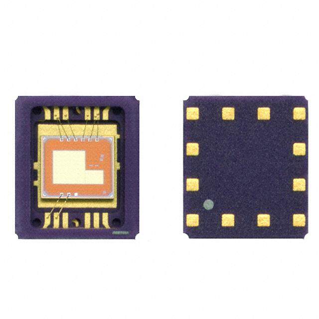
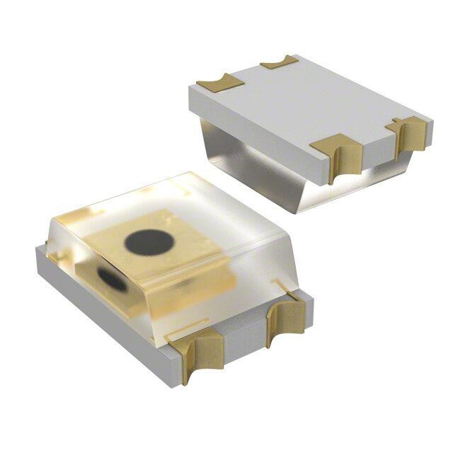
| 描述 | AMBIENT LIGHT SENSOR近程传感器 I2C Proximity Amb Light Sensor 3 LED |
| 产品分类 | |
| 品牌 | Silicon LabsSilicon Laboratories Inc |
| 产品手册 | |
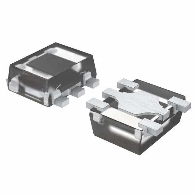
| 产品图片 |
|
| rohs | 符合RoHS无铅 / 符合限制有害物质指令(RoHS)规范要求 |
| 产品系列 | Silicon Labs Si1143-A11-GMR- |
| 数据手册 | |
| 产品型号 | SI1143-A11-GMRSi1143-A11-GMR |
| 产品种类 | 近程传感器 |
| 供应商器件封装 | 10-QFN(2x2) |
| 其它名称 | 336-2201-6 |
| 包装 | Digi-Reel® |
| 参考设计库 | http://www.digikey.com/rdl/4294959866/4294959865/738 |
| 商标 | Silicon Labs |
| 安装类型 | 表面贴装 |
| 安装风格 | SMD/SMT |
| 封装 | Reel |
| 封装/外壳 | 10-WFQFN |
| 封装/箱体 | QFN-10 |
| 工作温度 | -40°C ~ 85°C |
| 工厂包装数量 | 2500 |
| 带接近传感器 | 是 |
| 应用说明 | 点击此处下载产品Datasheet点击此处下载产品Datasheet点击此处下载产品Datasheet点击此处下载产品Datasheet点击此处下载产品Datasheet |
| 感应方式 | Optical |
| 感应距离 | 1 cm to 50 cm |
| 最大工作温度 | + 85 C |
| 最小工作温度 | - 40 C |
| 标准包装 | 1 |
| 波长 | - |
| 电压-电源 | 1.71 V ~ 3.6 V |
| 电源电压 | 1.71 V to 3.6 V |
| 电源电流 | 1.4 uA |
| 类型 | 环境 |
| 系列 | Si1143 |
| 设计资源 | |
| 输出类型 | I²C |
| 输出配置 | Digital |


- 商务部:美国ITC正式对集成电路等产品启动337调查
- 曝三星4nm工艺存在良率问题 高通将骁龙8 Gen1或转产台积电
- 太阳诱电将投资9.5亿元在常州建新厂生产MLCC 预计2023年完工
- 英特尔发布欧洲新工厂建设计划 深化IDM 2.0 战略
- 台积电先进制程称霸业界 有大客户加持明年业绩稳了
- 达到5530亿美元!SIA预计今年全球半导体销售额将创下新高
- 英特尔拟将自动驾驶子公司Mobileye上市 估值或超500亿美元
- 三星加码芯片和SET,合并消费电子和移动部门,撤换高东真等 CEO
- 三星电子宣布重大人事变动 还合并消费电子和移动部门
- 海关总署:前11个月进口集成电路产品价值2.52万亿元 增长14.8%

PDF Datasheet 数据手册内容提取
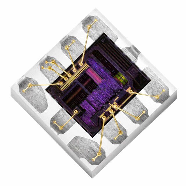
Si1141/42/43 2 PROXIMITY/AMBIENT LIGHT SENSOR IC WITH I C INTERFACE Features Pin Assignments Integrated infrared proximity detector Accurate lux measurements with IR Proximity detection adjustable from correction algorithm under 1cm up to 200cm Industry's lowest power consumption DNC Three independent LED drivers 1.71 to 3.6V supply voltage 10 15 current settings from 5.6mA to 9µA average current (LED pulsed SDA 1 9 LED1 360mA for each LED driver 25.6µs every 800ms at 180mA SCL 2 8 GND 25.6µs LED driver pulse width plus 3µA Si114x supply) QFN-10 50cm proximity range with single < 500nA standby current VDD 3 7 LED3/CVDD pulse (<3klx) 25.6µs LED “on” time keeps total INT 4 6 LED2/CVDD 15cm proximity range with single power consumption duty cycle low 5 pulse (>3klx) without compromising performance DNC Operates at up to 128klx (direct or noise immunity sunlight) Internal and external wake support High reflectance sensitivity Built-in voltage supply monitor and < 1µW/cm2 power-on reset controller High EMI immunity without shielded Serial communications packaging Up to 3.4Mbps data rate Integrated ambient light sensor Slave mode hardware address 100mlx resolution possible, decoding (0x5A) allowing operation under dark glass Small-outline 10-lead 2x2mm QFN 1 to 128klx dynamic range possible Temperature Range across two ADC range settings –40 to +85°C Applications Handsets Valve controls Heart rate monitoring Smoke detectors Pulse oximetry Touchless switches Wearables Touchless sliders Audio products Occupancy sensors Security panels Consumer electronics Tamper detection circuits Industrial automation Dispensers Display backlighting control Photo-interrupters Description The Si1141/42/43 is a low-power, reflectance-based, infrared proximity and ambient light sensor with I2C digital interface and programmable-event interrupt output. This touchless sensor IC includes an analog-to-digital converter, integrated high- sensitivity visible and infrared photodiodes, digital signal processor, and one, two, or three integrated infrared LED drivers with fifteen selectable drive levels. The Si1141/ 42/43 offers excellent performance under a wide dynamic range and a variety of light sources including direct sunlight. The Si1141/42/43 can also work under dark glass covers. The photodiode response and associated digital conversion circuitry provide excellent immunity to artificial light flicker noise and natural light flutter noise. With two or more LEDs, the Si1142/43 is capable of supporting multiple-axis proximity motion detection. The Si1141/42/43 devices are provided in a 10-lead 2x2mm QFN package and are capable of operation from 1.71 to 3.6V over the –40 to +85°C temperature range. Rev. 1.41 5/15 Copyright © 2015 by Silicon Laboratories Si1141/42/43
Si1141/42/43 Functional Block Diagram VDD Regulator LED1 LED Temp Drivers LED21 A ADC Filter LED32 M U Visible X Digital Sequencer & Control Logic Infrared INT SCL SDA I2C Registers Oscillator GND 1. Si1142 and Si1143 only. Must be tied to VDD with Si1141. 2. Si1143 only. Must be tied to VDD with Si1141 and Si1142. 3.3 V 30 ohm 5%, 1/16 W Host Si1141 SDA SDA LED1 SCL SCL GND VDD CVDD INT INT CVDD 15 µF, 20%, >6 V 0.1 uF Figure 1. Si1141 Basic Application 3.3 V 4.3 V No 30 ohm Pop 5%, 1/16 W Host Si1143 SDA LED1 SCL GND VDD LED3 INT LED2 22 uF, 20%, >6V 0.1 uF Figure 2. Si1143 Application with Three LEDs and Separate LED Power Supply Note: For more application examples, refer to “AN498: Si114x Designer’s Guide”. 2 Rev. 1.41
Si1141/42/43 TABLE OF CONTENTS Section Page 1. Electrical Specifications . . . . . . . . . . . . . . . . . . . . . . . . . . . . . . . . . . . . . . . . . . . . . . . . . . .4 1.1. Performance Tables . . . . . . . . . . . . . . . . . . . . . . . . . . . . . . . . . . . . . . . . . . . . . . . . . .4 1.2. Typical Performance Graphs . . . . . . . . . . . . . . . . . . . . . . . . . . . . . . . . . . . . . . . . . .10 2. Functional Description . . . . . . . . . . . . . . . . . . . . . . . . . . . . . . . . . . . . . . . . . . . . . . . . . . .12 2.1. Introduction . . . . . . . . . . . . . . . . . . . . . . . . . . . . . . . . . . . . . . . . . . . . . . . . . . . . . . . .12 2.2. Proximity Sensing (PS) . . . . . . . . . . . . . . . . . . . . . . . . . . . . . . . . . . . . . . . . . . . . . . .12 2.3. Ambient Light . . . . . . . . . . . . . . . . . . . . . . . . . . . . . . . . . . . . . . . . . . . . . . . . . . . . . .13 2.4. Host Interface . . . . . . . . . . . . . . . . . . . . . . . . . . . . . . . . . . . . . . . . . . . . . . . . . . . . . .14 3. Operational Modes . . . . . . . . . . . . . . . . . . . . . . . . . . . . . . . . . . . . . . . . . . . . . . . . . . . . . . .17 3.1. Off Mode . . . . . . . . . . . . . . . . . . . . . . . . . . . . . . . . . . . . . . . . . . . . . . . . . . . . . . . . . .17 3.2. Initialization Mode . . . . . . . . . . . . . . . . . . . . . . . . . . . . . . . . . . . . . . . . . . . . . . . . . . .17 3.3. Standby Mode . . . . . . . . . . . . . . . . . . . . . . . . . . . . . . . . . . . . . . . . . . . . . . . . . . . . . .17 3.4. Forced Conversion Mode . . . . . . . . . . . . . . . . . . . . . . . . . . . . . . . . . . . . . . . . . . . . .17 3.5. Autonomous Operation Mode . . . . . . . . . . . . . . . . . . . . . . . . . . . . . . . . . . . . . . . . . .18 4. Programming Guide . . . . . . . . . . . . . . . . . . . . . . . . . . . . . . . . . . . . . . . . . . . . . . . . . . . . . .19 4.1. Command and Response Structure . . . . . . . . . . . . . . . . . . . . . . . . . . . . . . . . . . . . .19 4.2. Command Protocol . . . . . . . . . . . . . . . . . . . . . . . . . . . . . . . . . . . . . . . . . . . . . . . . . .20 4.3. Resource Summary . . . . . . . . . . . . . . . . . . . . . . . . . . . . . . . . . . . . . . . . . . . . . . . . .23 4.4. Signal Path Software Model . . . . . . . . . . . . . . . . . . . . . . . . . . . . . . . . . . . . . . . . . . .28 4.5. I2C Registers . . . . . . . . . . . . . . . . . . . . . . . . . . . . . . . . . . . . . . . . . . . . . . . . . . . . . . .29 4.6. Parameter RAM . . . . . . . . . . . . . . . . . . . . . . . . . . . . . . . . . . . . . . . . . . . . . . . . . . . .52 5. Pin Descriptions . . . . . . . . . . . . . . . . . . . . . . . . . . . . . . . . . . . . . . . . . . . . . . . . . . . . . . . . .67 6. Ordering Guide . . . . . . . . . . . . . . . . . . . . . . . . . . . . . . . . . . . . . . . . . . . . . . . . . . . . . . . . . .68 7. Package Outline: 10-Pin QFN . . . . . . . . . . . . . . . . . . . . . . . . . . . . . . . . . . . . . . . . . . . . . .69 8. Suggested PCB Land Pattern . . . . . . . . . . . . . . . . . . . . . . . . . . . . . . . . . . . . . . . . . . . . . .71 Document Change List . . . . . . . . . . . . . . . . . . . . . . . . . . . . . . . . . . . . . . . . . . . . . . . . . . . . .73 Contact Information . . . . . . . . . . . . . . . . . . . . . . . . . . . . . . . . . . . . . . . . . . . . . . . . . . . . . . . .75 Rev. 1.41 3
Si1141/42/43 1. Electrical Specifications 1.1. Performance Tables Table 1. Recommended Operating Conditions Parameter Symbol Test Condition Min Typ Max Unit V Supply Voltage V 1.71 — 3.6 V DD DD V OFF Supply Voltage V OFF mode –0.3 1.0 V DD DD_OFF V Supply Ripple Voltage V =3.3V — — 50 mVpp DD DD 1kHz–10MHz Operating Temperature T –40 25 85 °C SCL, SDA, Input High Logic I2C V x0.7 — V V VIH DD DD Voltage SCL, SDA Input Low Logic I2C 0 — V x0.3 V VIL DD Voltage PS Operation under Edc — — 128 klx Direct Sunlight IrLED Emission Wavelength l 750 850 950 nm IrLED Supply Voltage VLED IrLED V =1.0V nominal V — 4.3 V F DD IrLED Supply Ripple Voltage Applies if IrLEDs use separate supply rail 0–30kHz — — 250 mVpp 30kHz–100MHz — — 100 mVpp Start-Up Time V above 1.71V 25 — — ms DD LED3 Voltage Start-up V x0.77 — — V DD Table 2. Performance Characteristics1 Parameter Symbol Test Condition Min Typ Max Unit I OFF Mode I V < V (leakage from SCL, — 240 1000 nA DD off DD DD_OFF SDA, and INT not included) I Standby Mode I No ALS / PS Conversions — 150 500 nA DD sb No I2C Activity V =1.8V DD Notes: 1. Unless specifically stated in "Conditions", electrical data assumes ambient light levels < 1klx. 2. Proximity-detection performance may be degraded, especially when there is high optical crosstalk, if the LED supply and voltage drop allow the driver to saturate and current regulation is lost. 3. Guaranteed by design and characterization. 4. Represents the time during which the device is drawing a current equal to I for power estimation purposes. active Assumes default settings. 4 Rev. 1.41
Si1141/42/43 Table 2. Performance Characteristics1 (Continued) Parameter Symbol Test Condition Min Typ Max Unit I Standby Mode I No ALS / PS Conversions — 1.4 — µA DD sb No I2C Activity V =3.3V DD I Actively Measuring I Without LED influence, V =3.3V — 4.3 5.5 mA DD active DD Peak IDD while LED1, V =3.3V — 8 — mA DD LED2, or LED3 is Actively Driven LED Driver Saturation Vdd=1.71 to 3.6V mV Voltage2,3 PS_LEDn=0001 — 50 70 PS_LEDn=0010 — 60 105 PS_LEDn=0011 — 70 105 PS_LEDn=0100 — 80 105 PS_LEDn=0101 — 115 450 PS_LEDn=0110 — 150 450 PS_LEDn=0111 — 185 450 PS_LEDn=1000 — 220 450 PS_LEDn=1010 — 255 450 PS_LEDn=1010 — 290 450 PS_LEDn=1011 — 315 600 PS_LEDn=1100 — 340 600 PS_LEDn=1101 — 360 600 PS_LEDn=1110 — 385 600 PS_LEDn=1111 — 410 600 LED1, LED2, LED3 t — 25.6 30 µs PS Pulse Width LED1, LED2, LED3, V =3.3V –1 — 1 µA DD INT, SCL, SDA Leakage Current Notes: 1. Unless specifically stated in "Conditions", electrical data assumes ambient light levels < 1klx. 2. Proximity-detection performance may be degraded, especially when there is high optical crosstalk, if the LED supply and voltage drop allow the driver to saturate and current regulation is lost. 3. Guaranteed by design and characterization. 4. Represents the time during which the device is drawing a current equal to I for power estimation purposes. active Assumes default settings. Rev. 1.41 5
Si1141/42/43 Table 2. Performance Characteristics1 (Continued) Parameter Symbol Test Condition Min Typ Max Unit LED1, LED2, LED3 I V =3.3V, single drive mA LEDx DD Active Current V =1V, PS_LEDn=0001 3.5 5.6 7 LEDn V =1V, PS_LEDn=0010 — 11.2 — LEDn V =1V, PS_LEDn=0011 13 22.4 29 LEDn V =1 V, PS_LEDn=0100 — 45 — LEDn V =1V, PS_LEDn=0101 — 67 — LEDn V =1V, PS_LEDn=0110 — 90 — LEDn V =1V, PS_LEDn=0111 — 112 — LEDn V =1V, PS_LEDn=1000 — 135 — LEDn V =1V, PS_LEDn=1001 — 157 — LEDn V =1V, PS_LEDn=1010 — 180 — LEDn V =1V, PS_LEDn=1011 — 202 — LEDn V =1V, PS_LEDn=1100 — 224 — LEDn V =1V, PS_LEDn=1101 — 269 — LEDn V =1V, PS_LEDn=1110 — 314 — LEDn V =1V, PS_LEDn=1111 — 359 — LEDn Actively Measuring Single PS — 155 — µs Time4 ALS VIS + ALS IR — 285 — µs Two ALS plus three PS — 660 — µs Visible Photodiode Sunlight — 0.282 — ADC Response ALS_VIS_ADC_GAIN=0 counts/lux VIS_RANGE=0 2500K incandescent bulb — 0.319 — ADC ALS_VIS_ADC_GAIN=0 counts/lux VIS_RANGE=0 “Cool white” fluorescent — 0.146 — ADC ALS_VIS_ADC_GAIN=0 counts/lux VIS_RANGE=0 Infrared LED (875 nm) — 8.277 — ADC ALS_VIS_ADC_GAIN=0 counts.m2/ VIS_RANGE=0 W Notes: 1. Unless specifically stated in "Conditions", electrical data assumes ambient light levels < 1klx. 2. Proximity-detection performance may be degraded, especially when there is high optical crosstalk, if the LED supply and voltage drop allow the driver to saturate and current regulation is lost. 3. Guaranteed by design and characterization. 4. Represents the time during which the device is drawing a current equal to I for power estimation purposes. active Assumes default settings. 6 Rev. 1.41
Si1141/42/43 Table 2. Performance Characteristics1 (Continued) Parameter Symbol Test Condition Min Typ Max Unit Small Infrared Photodi- Sunlight — 2.44 — ADC ode Response ALS_IR_ADC_GAIN=0 counts/lux IR_RANGE=0 2500K incandescent bulb — 8.46 — ADC ALS_IR_ADC_GAIN=0 counts/lux IR_RANGE=0 “Cool white” fluorescent — 0.71 — ADC ALS_IR_ADC_GAIN=0 counts/lux IR_RANGE=0 Infrared LED (875 nm) — 452.38 — ADC ALS_IR_ADC_GAIN=0 counts.m2/ IR_RANGE=0 W Large Infrared Photodi- Sunlight — 14.07 — ADC ode Response PS_ADC_GAIN=0 counts/lux PS_RANGE=0 PS_ADC_MODE=0 2500K incandescent bulb — 50.47 — ADC PS_ADC_GAIN=0 counts/lux PS_RANGE=0 PS_ADC_MODE=0 “Cool white” fluorescent — 3.97 — ADC PS_ADC_GAIN=0 counts/lux PS_RANGE=0 PS_ADC_MODE=0 Infrared LED (875 nm) — 2734 — ADC PS_ADC_GAIN=0 counts.m2/ PS_RANGE=0 W PS_ADC_MODE=0 Visible Photodiode All gain settings — 7 — ADC Noise counts RMS Small Infrared Photodi- All gain settings — 1 — ADC ode Noise counts RMS Notes: 1. Unless specifically stated in "Conditions", electrical data assumes ambient light levels < 1klx. 2. Proximity-detection performance may be degraded, especially when there is high optical crosstalk, if the LED supply and voltage drop allow the driver to saturate and current regulation is lost. 3. Guaranteed by design and characterization. 4. Represents the time during which the device is drawing a current equal to I for power estimation purposes. active Assumes default settings. Rev. 1.41 7
Si1141/42/43 Table 2. Performance Characteristics1 (Continued) Parameter Symbol Test Condition Min Typ Max Unit Large Infrared Photodi- All gain settings — 10 — ADC ode Noise counts RMS Visible Photodiode Off- VIS_RANGE=0 — — ADC set Drift ALS_VIS_ADC_GAIN=0 –0.3 counts/°C ALS_VIS_ADC_GAIN=1 –0.11 ALS_VIS_ADC_GAIN=2 –0.06 ALS_VIS_ADC_GAIN=3 –0.03 ALS_VIS_ADC_GAIN=4 –0.01 ALS_VIS_ADC_GAIN=5 –0.008 ALS_VIS_ADC_GAIN=6 –0.007 ALS_VIS_ADC_GAIN=7 –0.008 Small Infrared Photodi- IR_RANGE=0 — — ADC ode Offset Drift IR_GAIN=0 –0.3 counts/°C IR_GAIN=1 –0.06 IR_GAIN=2 –0.03 IR_GAIN=3 –0.01 SCL, SDA, INT Output V I=4mA, V > 2.0V — — V x 0.2 V OL DD DD Low Voltage I=4mA, V < 2.0V — — 0.4 V DD Temperature Sensor 25°C — 11136 — ADC Offset counts Temperature Sensor — 35 — ADC Gain counts/°C Notes: 1. Unless specifically stated in "Conditions", electrical data assumes ambient light levels < 1klx. 2. Proximity-detection performance may be degraded, especially when there is high optical crosstalk, if the LED supply and voltage drop allow the driver to saturate and current regulation is lost. 3. Guaranteed by design and characterization. 4. Represents the time during which the device is drawing a current equal to I for power estimation purposes. active Assumes default settings. 8 Rev. 1.41
Si1141/42/43 Table 3. I2C Timing Specifications Parameter Symbol Min Typ Max Unit Clock Frequency f 0.09 — 3.4 MHz SCL Clock Pulse Width Low t 160 — — ns LOW Clock Pulse Width High t 60 — — ns HIGH Rise Time t 10 — 40 ns R Fall Time t 10 — 40 ns F Start Condition Hold Time t 160 — — ns HD.STA Start Condition Setup Time t 160 — — ns SU.STA Input Data Setup Time t 10 — — ns SU.DAT Input Data Hold Time t 0 — — ns HD.DAT Stop Condition Setup Time t 160 — — ns SU.STO Table 4. Absolute Maximum Limits Parameter Test Condition Min Typ Max Unit V Supply Voltage –0.3 — 4 V DD Operating Temperature –40 — 85 °C Storage Temperature –65 — 85 °C LED1, LED2, LED3 Voltage at V =0V, T < 85°C –0.5 — 3.6 V DD A INT, SCL, SDA Voltage at V =0V, T < 85°C –0.5 — 3.6 V DD A Maximum total current through — — 500 mA LED1, LED2 and LED3 Maximum total current through — — 600 mA GND ESD Rating Human Body Model — — 2 kV Machine Model — — 225 V Charged-Device Model — — 2 kV Rev. 1.41 9
Si1141/42/43 1.2. Typical Performance Graphs Figure 3. Proximity response using Kodak gray cards, PS_RANGE = 0, PS_ADC_GAIN = 0 (single 25.6s LED pulse), ± 22°LED view angle, 850 nm, 22.5 mW/sr, no overlay, 5 mm LED center to Si114x center Figure 4. ALS variability with different light sources 10 Rev. 1.41
Si1141/42/43 Figure 5. View angle, large photodiode rotated around the pin-5/pin-10 (“vertical”) axis Figure 6. View angle, large photodiode rotated around “horizontal”axis and small photodiode rotated around either axis Rev. 1.41 11
Si1141/42/43 2. Functional Description 2.1. Introduction The Si1141/42/43 is an active optical reflectance proximity detector and ambient light sensor whose operational state is controlled through registers accessible through the I2C interface. The host can command the Si1141/42/43 to initiate on-demand proximity detection or ambient light sensing. The host can also place the Si1141/42/43 in an autonomous operational state where it performs measurements at set intervals and interrupts the host either after each measurement is completed or whenever a set threshold has been crossed. This results in an overall system power saving allowing the host controller to operate longer in its sleep state instead of polling the Si1141/42/43. For more details, refer to “AN498: Si114x Designer's Guide”. 2.2. Proximity Sensing (PS) The Si1141/42/43 has been optimized for use as either a dual-port or single-port active reflection proximity detector. Over distances of less than 50cm, the dual-port active reflection proximity detector has significant advantages over single-port, motion-based infrared systems, which are only good for triggered events. Motion- based infrared detectors identify objects within proximity, but only if they are moving. Single-port motion-based infrared systems are ambiguous about stationary objects even if they are within the proximity field. The Si1141/42/ 43 can reliably detect an object entering or exiting a specified proximity field, even if the object is not moving or is moving very slowly. However, beyond about 30–50cm, even with good optical isolation, single-port signal processing may be required due to static reflections from nearby objects, such as table tops, walls, etc. If motion detection is acceptable, the Si1141/42/43 can achieve ranges of up to 50cm, through a single product window. For small objects, the drop in reflectance is as much as the fourth power of the distance. This means that there is less range ambiguity than with passive motion-based devices. For example, a sixteenfold change in an object's reflectance means only a fifty-percent drop in detection range. The Si1143 can drive three separate infrared LEDs. When the three infrared LEDs are placed in an L-shaped configuration, it is possible to triangulate an object within the three-dimensional proximity field. Thus, a touchless user interface can be implemented with the aid of host software. The Si1141/42/43 can initiate proximity sense measurements when explicitly commanded by the host or periodically through an autonomous process. Refer to "3. Operational Modes" on page 17 for additional details of the Si1141/42/43's Operational Modes. Whenever it is time to make a PS measurement, the Si1141/42/43 makes up to three measurements, depending on what is enabled in the CHLIST parameter. Other ADC parameters for these measurements can also be modified to allow proper operation under different ambient light conditions. The LED choice is programmable for each of these three measurements. By default, each measurement turns on a single LED driver. However, the order of measurements can be easily reversed or even have all LEDs turned on at the same time. Optionally, each proximity measurement can be compared against a host-programmable threshold. With threshold settings for each PS channel, it is also possible for the Si1141/42/43 to notify the host whenever the threshold has been crossed. This reduces the number of interrupts to the host, aiding in efficient software algorithms. The Si1141/42/43 can also generate an interrupt after a complete set of proximity measurements, ignoring any threshold settings. To support different power usage cases dynamically, the infrared LED current of each output is independently programmable. The current can be programmed anywhere from a few to several hundred milliamps. Therefore, the host can optimize for proximity detection performance or for power saving dynamically. This feature can be useful since it allows the host to reduce the LED current once an object has entered a proximity sphere, and the object can still be tracked at a lower current setting. Finally, the flexible current settings make it possible to control the infrared LED currents with a controlled current sink, resulting in higher precision. The ADC properties are programmable. For indoor operation, the ADC should be configured for low signal range for best reflectance sensitivity. When under high ambient conditions, the ADC should be configured for high signal level range operation. 12 Rev. 1.41
Si1141/42/43 When operating in the lower signal range, it is possible to saturate the ADC when the ambient light level is high. Any overflow condition is reported in the RESPONSE register, and the corresponding data registers report a value of 0xFFFF. The host can then adjust the ADC sensitivity. Note however that the overflow condition is not sticky. If the light levels return to a range within the capabilities of the ADC, the corresponding data registers begin to operate normally. However, the RESPONSE register will continue to hold the overflow condition until a NOP command is received. Even if the RESPONSE register has an overflow condition, commands are still accepted and processed. Proximity detection ranges beyond 50cm and up to several meters can be achieved without lensing by selecting a longer integration time. The detection range may be increased further, even with high ambient light, by averaging multiple measurements. Refer to “AN498: Si114x Designer's Guide” for more details. 2.3. Ambient Light The Si1141/42/43 has photodiodes capable of measuring both visible and infrared light. However, the visible photodiode is also influenced by infrared light. The measurement of illuminance requires the same spectral response as the human eye. If an accurate lux measurement is desired, the extra IR response of the visible-light photodiode must be compensated. Therefore, to allow the host to make corrections to the infrared light’s influence, the Si1141/42/43 reports the infrared light measurement on a separate channel. The separate visible and IR photodiodes lend themselves to a variety of algorithmic solutions. The host can then take these two measurements and run an algorithm to derive an equivalent lux level as perceived by a human eye. Having the IR correction algorithm running in the host allows for the most flexibility in adjusting for system-dependent variables. For example, if the glass used in the system blocks visible light more than infrared light, the IR correction needs to be adjusted. If the host is not making any infrared corrections, the infrared measurement can be turned off in the CHLIST parameter. By default, the measurement parameters are optimized for indoor ambient light levels where it is possible to detect light levels as low as 6lx. For operation under direct sunlight, the ADC can be programmed to operate in a high signal operation so that it is possible to measure direct sunlight without overflowing the 16-bit result. For low-light applications, it is possible to increase the ADC integration time. Normally, the integration time is 25.6µs. By increasing this integration time to 410µs, the ADC can detect light levels as low as 1lx. The ADC can be programmed with an integration time as high as 3.28ms, allowing measurement to 100mlx light levels. The ADC integration time for the Visible Light Ambient measurement can be programmed independently of the ADC integration time of the Infrared Light Ambient measurement. The independent ADC parameters allow operation under glass covers having a higher transmittance to Infrared Light than Visible Light. When operating in the lower signal range, or when the integration time is increased, it is possible to saturate the ADC when the ambient light suddenly increases. Any overflow condition is reported in the RESPONSE register, and the corresponding data registers report a value of 0xFFFF. Based on either of these two overflow indicators, the host can adjust the ADC sensitivity. However, the overflow condition is not sticky. If the light levels return to a range within the capabilities of the ADC, the corresponding data registers begin to operate normally. The RESPONSE register will continue to hold the overflow condition until a NOP command is received. Even if the RESPONSE register has an overflow condition, commands are still accepted and processed. The Si1141/42/43 can initiate ALS measurements either when explicitly commanded by the host or periodically through an autonomous process. Refer to "3. Operational Modes" on page 17 for additional details of the Si1141/ 42/43's Operational Modes. The conversion frequency setting is programmable and independent of the Proximity Sensor. This allows the Proximity Sensor and Ambient Light sensor to operate at different conversion rates, increasing host control over the Si1141/42/43. When operating autonomously, the ALS has a slightly different interrupt structure compared to the Proximity Sensor. An interrupt can be generated to the host on every sample, or when the ambient light has changed. The “Ambient Light Changed” interrupt is accomplished through two thresholds working together to implement a window. As long as the ambient light stays within the window defined by the two thresholds, the host is not interrupted. When the ambient light changes and either threshold is crossed, an interrupt is sent to the host, thereby allowing the host notification that the ambient light has changed. This can be used by the host to trigger a recalculation of the lux values. Rev. 1.41 13
Si1141/42/43 The window can be applied to either the Visible Ambient Measurement, or the Infrared Ambient Measurement, but not both. However, monitoring the ambient change in either channel should allow notification that the ambient light level has changed. Normalized(cid:3)Photodiode(cid:3)Response 1 0.9 VIS IR 0.8 0.7 0.6 0.5 0.4 0.3 0.2 0.1 0 250 350 450 550 650 750 850 950 1050 Wavelength(cid:3)(nm) Figure 7. Photodiode Spectral Response to Visible and Infrared Light (Indicative) 2.4. Host Interface The host interface to the Si1141/42/43 consists of three pins: SCL SDA INT SCL and SDA are standard open-drain pins as required for I2C operation. The Si1141/42/43 asserts the INT pin to interrupt the host processor. The INT pin is an open-drain output. A pull-up resistor is needed for proper operation. As an open-drain output, it can be shared with other open-drain interrupt sources in the system. For proper operation, the Si1141/42/43 is expected to fully complete its Initialization Mode prior to any activity on the I2C. The INT, SCL, and SDA pins are designed so that it is possible for the Si1141/42/43 to enter the Off Mode by software command without interfering with normal operation of other I2C devices on the bus. The Si1141/42/43 I2C slave address is 0x5A. The Si1141/42/43 also responds to the global address (0x00) and the global reset command (0x06). Only 7-bit I2C addressing is supported; 10-bit I2C addressing is not supported. Conceptually, the I2C interface allows access to the Si1141/42/43 internal registers. Table15 on page29 is a summary of these registers. An I2C write access always begins with a start (or restart) condition. The first byte after the start condition is the I2C address and a read-write bit. The second byte specifies the starting address of the Si1141/42/43 internal register. Subsequent bytes are written to the Si1141/42/43 internal register sequentially until a stop condition is encountered. An I2C write access with only two bytes is typically used to set up the Si1141/42/43 internal address in preparation for an I2C read. The I2C read access, like the I2C write access, begins with a start or restart condition. In an I2C read, the I2C master then continues to clock SCK to allow the Si1141/42/43 to drive the I2C with the internal register contents. 14 Rev. 1.41
Si1141/42/43 The Si1141/42/43 also supports burst reads and burst writes. The burst read is useful in collecting contiguous, sequential registers. The Si1141/42/43 register map was designed to optimize for burst reads for interrupt handlers, and the burst writes are designed to facilitate rapid programming of commonly used fields, such as thresholds registers. The internal register address is a six-bit (bit 5 to bit 0) plus an Autoincrement Disable (on bit 6). The Autoincrement Disable is turned off by default. Disabling the autoincrementing feature allows the host to poll any single internal register repeatedly without having to keep updating the Si1141/42/43 internal address every time the register is read. It is recommended that the host should read PS or ALS measurements (in the I2C Register Map) when the Si1141/ 42/43 asserts INT. Although the host can read any of the Si1141/42/43's I2C registers at any time, care must be taken when reading 2-byte measurements outside the context of an interrupt handler. The host could be reading part of the 2-byte measurement when the internal sequencer is updating that same measurement coincidentally. When this happens, the host could be reading a hybrid 2-byte quantity whose high byte and low byte are parts of different samples. If the host must read these 2-byte registers outside the context of an interrupt handler, the host should “double-check” a measurement if the measurement deviates significantly from a previous reading. I2C Broadcast Reset: The I2C Broadcast Reset should be sent prior to any I2C register access to the Si114x. If any I2C register or parameter has already been written to the Si114x when the I2C Broadcast Reset is issued, the host must send a reset command and reinitialize the Si114x completely. SCL SDA SLA6 SLA5-0 R/W D7 D6-0 START Slave Address + R/W ACK Data Byte NACK STOP Figure 8. I2C Bit Timing Diagram Figure 9. Host Interface Single Write Figure 10. Host Interface Single Read Figure 11. Host Interface Burst Write Figure 12. Host Interface Burst Read Rev. 1.41 15
Si1141/42/43 Figure 13. Si1141/42/43 REG ADDRESS Format Notes: Gray boxes are driven by the host to the Si1141/42/43 White boxes are driven by the Si1141/42/43 to the host A=ACK or “acknowledge” N=NACK or “no acknowledge” S=START condition Sr=repeat START condition P=STOP condition AI=Disable Auto Increment when set 16 Rev. 1.41
Si1141/42/43 3. Operational Modes The Si1141/42/43 can be in one of many operational modes at any one time. It is important to consider the operational mode since the mode has an impact on the overall power consumption of the Si1141/42/43. The various modes are: Off Mode Initialization Mode Standby Mode Forced Conversion Mode Autonomous Mode 3.1. Off Mode The Si1141/42/43 is in the Off Mode when V is either not connected to a power supply or if the V voltage is DD DD below the stated VDD_OFF voltage described in the electrical specifications. As long as the parameters stated in Table4, “Absolute Maximum Limits,” on page9 are not violated, no current will flow through the Si1141/42/43. In the Off Mode, the Si1141/42/43 SCL and SDA pins do not interfere with other I2C devices on the bus. The LED pins will not draw current through the infrared diodes. Keeping V less than VDD_OFF is not intended as a method of DD achieving lowest system current draw. The reason is that the ESD protection devices on the SCL, SDA and INT pins also from a current path through V . If V is grounded for example, then, current flow from system power to DD DD system ground through the SCL, SDA and INT pull-up resistors and the ESD protection devices. Allowing V to be less than VDD_OFF is intended to serve as a hardware method of resetting the Si1141/42/43 DD without a dedicated reset pin. The Si1141/42/43 can also reenter the Off Mode upon receipt of either a general I2C reset or if a software reset sequence is initiated. When one of these software methods is used to enter the Off Mode, the Si1141/42/43 typically proceeds directly from the Off Mode to the Initialization Mode. 3.2. Initialization Mode When power is applied to V and is greater than the minimum V Supply Voltage stated in Table1, DD DD “Recommended Operating Conditions,” on page4, the Si1141/42/43 enters its Initialization Mode. In the Initialization Mode, the Si1141/42/43 performs its initial startup sequence. Since the I2C may not yet be active, it is recommended that no I2C activity occur during this brief Initialization Mode period. The “Start-up time” specification in Table1 is the minimum recommended time the host needs to wait before sending any I2C accesses following a power-up sequence. After Initialization Mode has completed, the Si1141/42/43 enters Standby Mode. The host must write 0x17 to the HW_KEY register for proper operation. 3.3. Standby Mode The Si1141/42/43 spends most of its time in Standby Mode. After the Si1141/42/43 completes the Initialization Mode sequence, it enters Standby mode. While in Standby Mode, the Si1141/42/43 does not perform any Ambient Light measurements or Proximity Detection functions. However, the I2C interface is active and ready to accept reads and writes to the Si1141/42/43 registers. The internal Digital Sequence Controller is in its sleep state and does not draw much power. In addition, the INT output retains its state until it is cleared by the host. I2C accesses do not necessarily cause the Si1141/42/43 to exit the Standby Mode. For example, reading Si1141/ 42/43 registers is accomplished without needing the Digital Sequence Controller to wake from its sleep state. 3.4. Forced Conversion Mode The Si1141/42/43 can operate in Forced Conversion Mode under the specific command of the host processor. The Forced Conversion Mode is entered if either the ALS_FORCE or the PS_FORCE command is sent. Upon completion of the conversion, the Si1141/42/43 can generate an interrupt to the host if the corresponding interrupt is enabled. It is possible to initiate both an ALS and multiple PS measurements with one command register write access by using the PSALS_FORCE command. Rev. 1.41 17
Si1141/42/43 3.5. Autonomous Operation Mode The Si1141/42/43 can be placed in the Autonomous Operation Mode where measurements are performed automatically without requiring an explicit host command for every measurement. The PS_AUTO, ALS_AUTO and PSALS_AUTO commands are used to place the Si1141/42/43 in the Autonomous Operation Mode. The Si1141/42/43 updates the I2C registers for PS and ALS automatically. Each measurement is allocated a 16-bit register in the I2C map. It is possible to operate the Si1141/42/43 without interrupts. When doing so, the host poll rate must be at least twice the frequency of the conversion rates for the host to always receive a new measurement. The host can also choose to be notified when these new measurements are available by enabling interrupts. The conversion frequencies for the PS and ALS measurements are set up by the host prior to the PS_AUTO, ALS_AUTO, or PSALS_AUTO commands. The host can set a PS conversion frequency different from the ALS conversion frequency. However, they both need to be a multiple of the base conversion frequency in the MEAS_RATE register in the I2C map. The Si1141/42/43 can interrupt the host when the PS or ALS measurements reach a pre-set threshold. To assist in the handling of interrupts the registers are arranged so that the interrupt handler can perform an I2C burst read operation to read the necessary registers, beginning with the interrupt status register, and cycle through the ALS data registers followed by the individual Proximity readings. 18 Rev. 1.41
Si1141/42/43 4. Programming Guide 4.1. Command and Response Structure All Si1141/42/43 I2C registers (except writes to the COMMAND register) are read or written without waking up the internal sequencer. A complete list of the I2C registers can be found in "4.5. I2C Registers" on page 29. In addition to the I2C Registers, RAM parameters are memory locations maintained by the internal sequencer. These RAM Parameters are accessible through a Command Protocol (see "4.6. Parameter RAM" on page 52). A complete list of the RAM Parameters can be found in "4.6. Parameter RAM" on page 52. The Si1141/42/43 can operate either in Forced Measurement or Autonomous Mode. When in Forced Measurement mode, the Si1141/42/43 does not make any measurements unless the host specifically requests the Si1141/42/43 to do so via specific commands (refer to the Section 3.2). The CHLIST parameter needs to be written so that the Si1141/42/43 would know which measurements to make. The parameter MEAS_RATE, when zero, places the internal sequencer in Forced Measurement mode. When in Forced Measurement mode, the internal sequencer wakes up only when the host writes to the COMMAND register. The power consumption is lowest in Forced Measurement mode (MEAS_RATE=0). The Si1141/42/43 operates in Autonomous Operation mode when MEAS_RATE is non-zero. The MEAS_RATE represents the time interval at which the Si1141/42/43 wakes up periodically. Once the internal sequencer has awoken, the sequencer manages an internal PS Counter and ALS Counter based on the PS_RATE and ALS_RATE registers. When the internal PS counter has expired, up to three proximity measurements are made (PS1, PS2 and PS3) depending on which measurements are enabled via the upper bits of the CHLIST Parameter. All three PS measurements are performed, in sequence, beginning with the PS1 measurement channel. In the same way, when the ALS counter has expired, up to three measurements are made (ALS_VIS, ALS_IR and AUX) depending on which measurements are enabled via the upper bits of the CHLIST Parameter. All three measurements are made in the following sequence: ALS_VIS, ALS_IR and AUX. PS_RATE and ALS_RATE are normally non-zero. A value of zero in PS_RATE or ALS_RATE causes the internal sequencer to never perform that measurement group. Typically, PS_RATE or ALS_RATE represents a value of one. A value of one essentially states that the specific measurement group is made every time the device wakes up. It is possible for both the PS Counter and ALS Counter to both expire at the same time. When that occurs, the PS measurements are performed before the ALS measurements. When all measurements have been made, the internal sequencer goes back to sleep until next time, as dictated by the MEAS_RATE parameter. The operation of the Si1141/42/43 can be described as two measurement groups bound by some common factors. The PS Measurement group consists of the three PS measurements while the ALS Measurement group consists of the Visible Light Ambient Measurement (ALS_VIS), the Infrared Light Ambient Measurement (ALS_IR) and the Auxiliary measurement (AUX). Each measurement group has three measurements each. The Channel List (CHLIST) parameter enables the specific measurements for that measurement grouping. Each measurement (PS1, PS2, PS3, ALS_VIS, ALS_IR, AUX) are controlled through a combination of I2C Register or Parameter RAM. Tables 7 to 9 below summarize the properties and resources used for each measurement. Rev. 1.41 19
Si1141/42/43 4.2. Command Protocol The I2C map implements a bidirectional message box between the host and the Si1141/42/43 Sequencer. Host- writable I2C registers facilitate host-to-Si1141/42/43 communication, while read-only I2C registers are used for Si1141/42/43-to-host communication. Unlike the other host-writable I2C registers, the COMMAND register causes the internal sequencer to wake up from Standby mode to process the host request. When a command is executed, the RESPONSE register is updated. Typically, when there is no error, the upper four bits are zeroes. To allow command tracking, the lower four bits implement a 4-bit circular counter. In general, if the upper nibble of the RESPONSE register is non-zero, this indicates an error or the need for special processing. The PARAM_WR and PARAM_RD registers are additional mailbox registers. In addition to the registers in the I2C map, there are environmental parameters accessible through the Command/ Response interface. These parameters are stored in the internal ram space. These parameters generally take more I2C accesses to read and write. The Parameter RAM is described in "4.6. Parameter RAM" on page 52. For every write to the Command register, the following sequence is required: 1. Write 0x00 to Command register to clear the Response register. 2. Read Response register and verify contents are 0x00. 3. Write Command value from Table5 into Command register. 4. Read the Response register and verify contents are now non-zero. If contents are still 0x00, repeat this step. Note: Step 4 is not applicable to the Reset Command because the device will reset itself and does not increment the Response register after reset. No Commands should be issued to the device for at least 1 ms after a Reset is issued. The Response register will be incremented upon the successful completion of a Command. If the Response register remains 0x00 for over 25 ms after the Command write, the entire Command process should be repeated from Step 1. Table 5. Command Register Summary COMMAND Register PARAM_W PARAM_RD Error Code in Description R Register Register RESPONSE Register Name Encoding PARAM_QUERY 100 aaaaa — nnnn nnnn Reads the parameter pointed to by bitfield [4:0] and writes value to PARAM_RD. See Table10 for parameters. PARAM_SET 101 aaaaa dddd nnnn nnnn Sets parameter pointed by bit- dddd field [4:0] with value in PARAM_WR, and writes value out to PARAM_RD. See Table10 for parameters. PARAM_AND 110 aaaaa dddd nnnn nnnn Performs a bit-wise AND dddd between PARAM_WR and Parameter pointed by bitfield [4:0], writes updated value to PARAM_RD. See Table10 for parameters. 20 Rev. 1.41
Si1141/42/43 Table 5. Command Register Summary (Continued) COMMAND Register PARAM_W PARAM_RD Error Code in Description R Register Register RESPONSE Register Name Encoding PARAM_OR 111 aaaaa dddd nnnn nnnn Performs a bit-wise OR of dddd PARAM_WR and parameter pointed by bitfield [4:0], writes updated value to PARAM_RD. See Table10 for parameters. NOP 000 00000 — — Forces a zero into the RESPONSE register RESET 000 00001 — — Performs a software reset of the firmware BUSADDR 000 00010 — — — Modifies I2C address Reserved 000 00011 — — — — Reserved 000 00100 — — — — PS_FORCE 000 00101 — — Forces a single PS measure- ment ALS_FORCE 000 00110 — — Forces a single ALS measure- ment PSALS_FORCE 000 00111 — — Forces a single PS and ALS measurement Reserved 000 01000 — — — — PS_PAUSE 000 01001 — — Pauses autonomous PS ALS_PAUSE 000 01010 — — Pauses autonomous ALS PSALS_PAUSE 000 01011 — — Pauses PS and ALS Reserved 000 01100 — — — PS_AUTO 000 01101 — — Starts/Restarts an autonomous PS Loop ALS_AUTO 000 01110 — — Starts/Restarts an autonomous ALS Loop PSALS_AUTO 000 01111 — — Starts/Restarts autonomous ALS and PS loop Reserved 000 1xxxx — — — — Rev. 1.41 21
Si1141/42/43 Table 6. Response Register Error Codes RESPONSE Register Description 0000 cccc NO_ERROR. The lower bit is a circular counter and is incremented every time a command has completed. This allows the host to keep track of commands sent to the Si1141/42/43. The circular counter may be cleared using the NOP command. 1000 0000 INVALID_SETTING. An invalid setting was encountered. Clear using the NOP command. 1000 1000 PS1_ADC_OVERFLOW. Indicates proximity channel one conversion overflow. 1000 1001 PS2_ADC_OVERFLOW. Indicates proximity channel two conversion overflow. 1000 1010 PS3_ADC_OVERFLOW. Indicates proximity channel three conversion overflow. 1000 1100 ALS_VIS_ADC_OVERFLOW. Indicates visible ambient light channel conversion overflow. 1000 1101 ALS_IR_ADC_OVERFLOW. Indicates infrared ambient light channel conversion overflow. 1000 1110 AUX_ADC_OVERFLOW. Indicates auxiliary channel conversion overflow. 22 Rev. 1.41
Si1141/42/43 4.3. Resource Summary Table 7. Resource Summary for Interrupts and Threshold Checking Measurement Channel Interrupt Status Threshold Threshold History Autonomous Measurement Interrupt Enable Interrupt Mode Channel Enable Output Registers Hysteresis Checking Time Base Proximity EN_PS PS1_INT in PS1_IE in PS1_IM[1:0] in PS1_TH[7:0] PS_HYST[7: PS_HIS- MEAS_RATE[ PS_RATE[7: Sense 1 1 in IRQ_STA- IRQ_EN- IRQ_- 0] TORY[7:0] 7:0] 0] CHLIST TUS[2] ABLE[2] MODE1[5:4] [0] Proximity EN_PS PS2_INT in PS2_IE in PS2_IM[1:0] in PS2_TH[7:0] Sense 2 2 in IRQ_STA- IRQ_EN- IRQ_- CHLIST TUS[3] ABLE[3] MODE1[7:6] [1] Proximity EN_PS PS3_INT in PS3_EN in PS3_IM[1:0] in PS3_TH[7:0] Sense 3 3 in IRQ_STA- IRQ_EN- IRQ_- CHLIST TUS[4] ABLE[4] MODE2[1:0] [2] ALS Visible EN_AL ALS_INT[1:0] ALS_IE[1:0] in ALS_IM[2:0] in ALS_LOW_TH[7 ALS_HYST[ ALS_HIS- ALS_RATE[ S_VIS in IRQ_STA- IRQ_EN- IRQ_- :0] / 7:0] TORY[7:0] 7:0] in TUS[1:0] ABLE[1:0] MODE1[2:0] ALS_HI_TH[7:0] CHLIST [4] ALS IR EN_AL S_IR in CHLIST [5] Auxiliary EN_AU — — — — — — Measure- X in ment CHLIST [6] Rev. 1.41 23
Si1141/42/43 Table 8. Resource Summary for LED Choice and ADC Parameters Measure LED ADC Input ADC Recovery ADC High ADC Clock ADC ADC ment ADC Mode ADC Output Selection Source Count Signal Mode Divider Alignment Offset Channel Proximity PS1_LED[2: PS_ADC_- PS1_DA- PS1_ADC- PS_ADC_REC in PS_RANGE in PS_AD- PS1_ALIGN ADC_ Sense 1 0] in MODE TA1[7:0] / MUX[7:0] PS_AD- PS_ADC_- C_GAIN[3:0] in PS_EN- OFFSET PSLED12_S in PS1_DA- C_COUNTER MISC[5] CODING[4] [7:0] ELECT[2:0] PS_ADC_- TA0[7:0] [6:4] MISC[2] Proximity PS2_LED[2: PS2_DA- PS2_ADC- PS2_ALIGN Sense 2 0] in TA1[7:0] / MUX[7:0] in PS_EN- PSLED12_S PS2_DA- CODING[5] ELECT[6:4] TA0[7:0] Proximity PS3_LED[2: PS3_DA- PS3_ADC- PS3_ALIGN Sense 3 0] in TA1[7:0] / MUX[7:0] in PS_EN- PSLED3_SE PS3_DA- CODING[6] LECT[2:0] TA0[7:0] ALS Visi- — — ALS_VIS_- VIS_ADC_REC VIS_RANGE in ALS_VIS_AD- ALS_VIS_AL ble DATA1 / in ALS_VIS_AD- ALS_VIS_AD- C_GAIN [3:0] IGN in ALS_VIS_- C_COUNTER C_MISC[5] ALS_EN- DATA0 [6:4] CODING[4] ALS IR ALS_IR_DA- IR_ADC_REC in IR_RANGE in ALS_IR_AD- ALS_IR_ALI TA1[7:0] / ALS_IR_AD- ALS_IR_ADC_- C_GAIN [3:0] GN in ALS_IR_DA- C_COUNTER MISC[5] ALS_EN- TA0[7:0] [6:4] CODING[5] Auxiliary AUX_DA- AUX_ADC- — — — — Measure- TA1[7:0] / MUX[7:0] ment AUX_DA- TA0[7:0] 24 Rev. 1.41
Si1141/42/43 Table 9. Resource Summary for Hardware Pins Analog Voltage Input Pin Name LED Current Drive Output Drive Disable Enable LED1 LED1_I in PSLED12[3:0] ANA_IN_KEY[31:0] LED2 LED2_I in PSLED12[7:4] HW_KEY[7:0] ANA_IN_KEY[31:0] LED3 LED3_I in PSLED3[3:0] HW_KEY[7:0] INT INT_OE in INT_CFG[0] ANA_IN_KEY[31:0] The interrupts of the Si1141/42/43 are controlled through the INT_CFG, IRQ_ENABLE, IRQ_MODE1, IRQ_MODE2 and IRQ_STATUS registers. The INT hardware pin is enabled through the INT_OE bit in the INT_CFG register. The hardware essentially performs an AND function between the IRQ_ENABLE register and IRQ_STATUS register. After this AND function, if any bits are set, the INT pin is asserted. The INT_MODE bit in the INT_CFG register is conceptually a method of determining how the INT pin is deasserted. When INT_MODE = 0, the host is responsible for clearing the interrupt by writing to the IRQ_STATUS register. When the specific bits of the IRQ_STATUS register is written with '1', that specific IRQ_STATUS bit is cleared. Typically, the host software is expected to read the IRQ_STATUS register, stores a local copy, and then writes the same value back to the IRQ_STATUS to clear the interrupt source. Unless specifically stated, INT_MODE should be zero for normal interrupt handling operation. In summary, the INT_CFG register is normally written with '1'. The IRQ_MODE1, IRQ_MODE2 and IRQ_ENABLE registers work together to define how the internal sequencer sets bits in the IRQ_STATUS register (and as a consequence, asserting the INT pin). The PS1 interrupts are described in Table 10. The PS2 interrupts are described in Table11. The PS3 interrupts are described in Table12. The ALS interrupts are described in Table13, and the Command Interface interrupts are described in Table14. Rev. 1.41 25
Si1141/42/43 Table 10. PS1 Channel Interrupt Resources IRQ_ENABLE[2] IRQ_MODE1[5:4] Description PS1_IE PS1_IM[1:0] 0 0 0 No PS1 Interrupts 1 0 0 PS1_INT set after every PS1 sample 1 0 1 PS1_INT set whenever PS1 threshold (PS1_TH) is crossed 1 1 1 PS1_INT set whenever PS1 sample is above PS1 threshold (PS1_TH) Note: There is hysteresis applied (PS_HYST) and history checking (PS_HISTORY). PS_HYST is encoded in 8-bit compressed format. In the Si114x, PS1_TH is also encoded in compressed format. Table 11. PS2 Channel Interrupt Resources IRQ_ENABLE[3] IRQ_MODE1[7:6] Description PS2_IE PS2_IM[1:0] 0 0 0 No PS2 Interrupts 1 0 0 PS2_INT set after every PS2 sample 1 0 1 PS2_INT set whenever PS2 threshold (PS2_TH) is crossed 1 1 1 PS2_INT set when PS2 sample is above PS2 threshold (PS2_TH) Note: There is hysteresis applied (PS_HYST) and history checking (PS_HISTORY). PS_HYST is encoded in 8-bit compressed format. In the Si114x, PS2_TH is also encoded in compressed format. Table 12. PS3 Channel Interrupt Resources IRQ_ENABLE[4] IRQ_MODE2[1:0] Description PS3_IE PS3_IM[1:0] 0 0 0 No PS3 Interrupts 1 0 0 PS3_INT set after every PS3 sample 1 0 1 PS3_INT set whenever PS3 threshold (PS3_TH) is crossed 1 1 1 PS3_INT set whenever PS3 sample is above PS3 threshold (PS3_TH) Note: There is hysteresis applied (PS_HYST) and history checking (PS_HISTORY). PS_HYST is encoded in 8-bit compressed format. In the Si114x, PS3_TH is also encoded in compressed format. 26 Rev. 1.41
Si1141/42/43 Table 13. Ambient Light Sensing Interrupt Resources IRQ_ENABLE[1:0] IRQ_MODE1[2:0] Description ALS_IE[1:0] ALS_IM[2:0] 0 0 0 0 0 No ALS Interrupts 0 1 0 0 0 ALS_INT [0] set after every ALS_VIS sample1 x 1 x 0 1 Monitors ALS_VIS, ALS_INT [0] upon exiting region between low and high thresholds (ALS_LOW_TH and ALS_HI_TH) 1 x 1 0 x Monitors ALS_VIS, ALS_INT [1] set upon entering region between low and high thresholds (ALS_LOW_TH and ALS_HI_TH) x 1 x 1 1 Monitors ALS_IR, ALS_INT [0] set upon exiting region between low and high thresholds (ALS_LOW_TH and ALS_HI_TH) 1 x 1 1 x Monitors ALS_IR, ALS_INT [1] set upon entering region between low and high thresholds (ALS_LOW_TH and ALS_HI_TH) Notes: 1. For ALS_IR channel, interrupts per sample is not possible without also enabling ALS_VIS 2. All other combinations are invalid and may result in unintended operation 3. There is hysteresis applied (ALS_TH) and history checking (ALS_HISTORY). ALS_HYST is encoded in 8-bit compressed format. 4. In the Si114x, ALS_LOW_TH and ALS_HI_TH are also encoded in compressed format. Table 14. Command Interrupt Resources IRQ_ENABLE[5] IRQ_MODE2[3:2] Description CMD_IE CMD_IM[1:0] 0 x 0 No CMD Interrupts 1 x 0 CMD_INT set when there is a new RESPONSE 1 x 1 CMD_INT set when there is a new error code in RESPONSE Rev. 1.41 27
Si1141/42/43 4.4. Signal Path Software Model The following diagram gives an overview of the signal paths, along with the I2C register and RAM Parameter bit fields that control them. Sections with detailed descriptions of the I2C registers and Parameter RAM follow. 5 4 3 2 1 PS1_ALIGN PS_RATE PS1_ADCMUX PS_ADC_REC PS_ADC_GAIN PS_RANGE Select ADC_OFFSET Offset D Ref. 023600xx2655Out AnalogRangeGainRecov. timeRateAlign Digital InSEunmable16 PS1_DATA D Vdd 0x75 EN_PS1 GND PS2_ALIGN PS_RATE PS2_ADCMUX PS_ADC_REC PS_ADC_GAIN PS_RANGE Select ADC_OFFSET Offset Ref. 023600xx2655Out AnalogRangeGainRecov. timeRateAlign Digital InSEunmable16 PS2_DATA Vdd 0x75 EN_PS2 GND PS3_ALIGN PS_RATE PS3_ADCMUX PS_ADC_REC C PS_ADC_GAIN C PS_RANGE Select ADC_OFFSET Offset LLaarrggee IIRR VdRdef. 0236000xxx267555Out AnalogRangeGainRecov. timeRateAlign Digital InSEunmable16 PS3_DATA EN_PS3 GND GND ALS_VIS_ALIGN ALS_RATE ALS_VIS_ADC_REC ALS_VIS_ADC_GAIN VIS_RANGE ADC_OFFSET Offset B AnalogRangeGainRecov. timeRateAlign Digital InSEunmable16 ALS_VIS_DATA B SSmmaallll vviissiibbllee EN_ALS_VIS ALS_IR_ALIGN ALS_RATE ALS_IR_ADC_REC GND ALS_IR_ADC_GAIN ALS_IR_ADCMUX IR_RANGE ADC_OFFSET Offset 03 SeOlecutt AnalogRangeGainRecov. timeRateAlign Digital InSEunmable16 ALS_IR_DATA SSmmaallll IIRR EN_ALS_IR A AUX_ADCMUX A GND ADC_OFFSET Offset Select Sum 16 AUX_DATA 0x65 16 TTeemmppeerraattuurree Out Analog Digital In sseennssoorr Vdd 0x75 Enable EN_AUX 5 4 3 2 1 Figure 14. Signal Path Programming Model 28 Rev. 1.41
Si1141/42/43 4.5. I2C Registers Table 15. I2C Register Summary I2C Register Address 7 6 5 4 3 2 1 0 Name PART_ID 0x00 PART_ID REV_ID 0x01 REV_ID SEQ_ID 0x02 SEQ_ID INT_CFG 0x03 INT_- INT_O MODE E IRQ_ENABLE 0x04 CMD_IE PS3_IE PS2_IE PS1_IE ALS_IE IRQ_MODE1 0x05 PS2_IM PS1_IM ALS_IM IRQ_MODE2 0x06 CMD_IM PS3_IM HW_KEY 0x07 HW_KEY MEAS_RATE 0x08 MEAS_RATE ALS_RATE 0x09 ALS_RATE PS_RATE 0x0A PS_RATE ALS_LOW_TH0 0x0B ALS_LOW_TH0 ALS_LOW_TH1 0x0C ALS_LOW_TH1 ALS_HI_TH0 0x0D ALS_HI_TH0 ALS_HI_TH1 0x0E ALS_HI_TH1 PS_LED21 0x0F LED2_I LED1_I PS_LED3 0x10 LED3_I PS1_TH0 0x11 PS1_TH0 PS1_TH1 0x12 PS1_TH1 PS2_TH0 0x13 PS2_TH0 PS2_TH1 0x14 PS2_TH1 PS3_TH0 0x15 PS3_TH0 PS3_TH1 0x16 PS3_TH1 PARAM_WR 0x17 PARAM_WR COMMAND 0x18 COMMAND RESPONSE 0x20 RESPONSE Rev. 1.41 29
Si1141/42/43 Table 15. I2C Register Summary (Continued) I2C Register Address 7 6 5 4 3 2 1 0 Name IRQ_STATUS 0x21 CMD_IN PS3_IN PS2_IN PS1_IN ALS_INT T T T T ALS_VIS_DATA0 0x22 ALS_VIS_DATA0 ALS_VIS_DATA1 0x23 ALS_VIS_DATA1 ALS_IR_DATA0 0x24 ALS_IR_DATA0 ALS_IR_DATA1 0x25 ALS_IR_DATA1 PS1_DATA0 0x26 PS1_DATA0 PS1_DATA1 0x27 PS1_DATA1 PS2_DATA0 0x28 PS2_DATA0 PS2_DATA1 0x29 PS2_DATA1 PS3_DATA0 0x2A PS3_DATA0 PS3_DATA1 0x2B PS3_DATA1 AUX_DATA0 0x2C AUX_DATA0 AUX_DATA1 0x2D AUX_DATA1 PARAM_RD 0x2E PARAM_RD CHIP_STAT 0x30 RUN- SUS- SLEEP NING PEND ANA_IN_KEY 0x3B– ANA_IN_KEY 0x3E 30 Rev. 1.41
Si1141/42/43 PART_ID @ 0x00 Bit 7 6 5 4 3 2 1 0 PART_ID Name R Type Reset value=0100 0001 (Si1141) Reset value=0100 0010 (Si1142) Reset value=0100 0011 (Si1143) REV_ID @ 0x1 Bit 7 6 5 4 3 2 1 0 Name REV_ID Type R Reset value=0000 0000 SEQ_ID @ 0x02 Bit 7 6 5 4 3 2 1 0 SEQ_ID Name R Type Reset value=0000 1000 Bit Name Function 7:0 SEQ_ID Sequencer Revision. 0x01 Si114x-A01 (MAJOR_SEQ=0, MINOR_SEQ=1) 0x02 Si114x-A02 (MAJOR_SEQ=0, MINOR_SEQ=2) 0x03 Si114x-A03 (MAJOR_SEQ=0, MINOR_SEQ=3) 0x08 Si114x-A10 (MAJOR_SEQ=1, MINOR_SEQ=0) 0x09 Si114x-A11 (MAJOR_SEQ=1, MINOR_SEQ=1) Rev. 1.41 31
Si1141/42/43 INT_CFG @ 0x03 Bit 7 6 5 4 3 2 1 0 INT_MODE INT_OE Name RW RW Type Reset value=0000 0000 Bit Name Function 7:2 Reserved Reserved. 1 INT_MODE Interrupt Mode. The INT_MODE describes how the bits in the IRQ_STATUS Registers are cleared. 0: The IRQ_STATUS Register bits are set by the internal sequencer and are sticky. It is the host's responsibility to clear the interrupt status bits in the IRQ_STATUS register to clear the interrupt. 1: If the Parameter Field PSx_IM=11, the internal sequencer clears the INT pin auto- matically. 0 INT_OE INT Output Enable. INT_OE controls the INT pin drive 0: INT pin is never driven 1: INT pin driven low whenever an IRQ_STATUS and its corresponding IRQ_ENABLE bits match 32 Rev. 1.41
Si1141/42/43 IRQ_ENABLE @ 0x04 Bit 7 6 5 4 3 2 1 0 CMD_IE PS3_IE PS2_IE PS1_IE ALS_IE Name RW RW RW RW RW Type Reset value=0000 0000 Bit Name Function 7:6 Reserved Reserved. 5 CMD_IE Command Interrupt Enable. Enables interrupts based on COMMAND/RESPONSE activity. 0: INT never asserts due to COMMAND/RESPONSE interface activity. 1: Assert INT pin whenever CMD_INT is set by the internal sequencer. 4 PS3_IE PS3 Interrupt Enable. Enables interrupts based on PS3 Channel Activity. 0: INT never asserts due to PS3 Channel activity. 1: Assert INT pin whenever PS3_INT is set by the internal sequencer. 3 PS2_IE PS2 Interrupt Enable. Enables interrupts based on PS2 Channel Activity. 0: INT never asserts due to PS2 Channel activity. 1: Assert INT pin whenever PS2_INT is set by the internal sequencer. 2 PS1_IE PS1 Interrupt Enable. Enables interrupts based on PS1 Channel Activity. 0: INT never asserts due to PS1 Channel activity. 1: Assert INT pin whenever PS1_INT is set by the internal sequencer. 1:0 ALS_IE ALS Interrupt Enable. Enables interrupts based on ALS Activity. 00: INT never asserts due to ALS activity. 1x: Assert INT pin whenever ALS_INT[1] bit is set by the internal sequencer. x1: Assert INT pin whenever ALS_INT[0] is set by the internal sequencer. Rev. 1.41 33
Si1141/42/43 IRQ_MODE1 @ 0x05 Bit 7 6 5 4 3 2 1 0 PS2_IM PS1_IM ALS_IM Name RW RW RW Type Reset value=0000 0000 Bit Name Function 7:6 PS2_IM PS2 Interrupt Mode applies only when PS2_IE is also set. 00: PS2_INT is set whenever a PS2 measurement has completed. 01: PS2_INT is set whenever the current PS2 measurement crosses the PS2_TH threshold. 11: PS2_INT is set whenever the current PS2 measurement is greater than the PS2_TH threshold. 5:4 PS1_IM PS1 Interrupt Mode applies only when PS1_IE is also set. 00: PS1_INT is set whenever a PS1 measurement has completed. 01: PS1_INT is set whenever the current PS1 measurement crosses the PS1_TH threshold. 11: PS1_INT is set whenever the current PS1 measurement is greater than the PS1_TH threshold. 3 Reserved Reserved. 2:0 ALS_IM ALS Interrupt Mode function is defined in conjunction with ALS_IE[1:0]. ALS_IE[1:0] / ALS_IM[2:0]: 00 / 000: Neither ALS_INT[1] nor ALS_INT[0] is ever set. 01 / 000: ALS_INT[0] sets after every ALS_VIS sample. x1 / x01: Monitors ALS_VIS channel, ALS_INT[0] asserts if measurement exits window between ALS_LOW_TH and ALS_HIGH_TH. x1 / x11: Monitors ALS_IR channel, ALS_INT[0] asserts if measurement exits window between ALS_LOW_TH and ALS_HIGH_TH. 1x /10x: Monitors ALS_VIS channel, ALS_INT[1] asserts if measurement enters win- dow between ALS_LOW_TH and ALS_HIGH_TH. 1x /11x: Monitors ALS_IR channel, ALS_INT[1] asserts if measurement enters window between ALS_LOW_TH and ALS_HIGH_TH. Note: The ALS_IM description apples only to sequencer revisions A03 or later. 34 Rev. 1.41
Si1141/42/43 IRQ_MODE2 @ 0x06 Bit 7 6 5 4 3 2 1 0 CMD_IM PS3_IM Name RW RW Type Reset value=0000 0000 Bit Name Function 7:4 Reserved Reserved. 3:2 CMD_IM Command Interrupt Mode applies only when CMD_IE is also set. 00: CMD_INT is set whenever the RESPONSE register is written. 01: CMD_INT is set whenever the RESPONSE register is written with an error code (MSB set). 1x: Reserved. 1:0 PS3_IM PS3 Interrupt Mode applies only when PS3_IE is also set. 00: PS3_INT is set whenever a PS3 measurement has completed. 01: PS3_INT is set whenever the current PS3 measurement crosses the PS3_TH threshold. 11: PS3_INT is set whenever the current PS3 measurement is greater than the PS3_TH threshold. HW_KEY @ 0x07 Bit 7 6 5 4 3 2 1 0 HW_KEY Name RW Type Reset value=0000 0000 Bit Name Function 7:0 HW_KEY The system must write the value 0x17 to this register for proper Si114x operation. Rev. 1.41 35
Si1141/42/43 MEAS_RATE @ 0x08 Bit 7 6 5 4 3 2 1 0 MEAS_RATE Name RW Type Reset value=0000 0000 Bit Name Function 7:0 MEAS_RATE MEAS_RATE is an 8-bit compressed value representing a 16-bit integer. The uncompressed 16-bit value, when multiplied by 31.25 us, represents the time dura- tion between wake-up periods where measurements are made. Example Values: 0x00: Turns off any internal oscillator and disables autonomous measurement. Use this setting to achieve lowest V current draw for systems making use of only DD forced measurements. 0x01-0x17: These values are not allowed. 0x84: The device wakes up every 10ms (0x140 x 31.25µs) 0x94: The device wakes up every 20ms (0x280 x 31.25µs) 0xB9: The device wakes up every 100ms (0x0C80 x 31.25µs) 0xDF: The device wakes up every 496ms (0x3E00 x 31.25µs) 0xFF: The device wakes up every 1.984seconds (0xF800 x 31.25µs) Please refer to “AN498: Si114x Designer’s Guide”, Section 5.4 “Compression Concept.” 36 Rev. 1.41
Si1141/42/43 ALS_RATE @ 0x09 Bit 7 6 5 4 3 2 1 0 ALS_RATE Name RW Type Reset value=0000 0000 Bit Name Function 7:0 ALS_RATE ALS_RATE is an 8-bit compressed value representing a 16-bit multiplier. This multi- plier, in conjunction with the MEAS_RATE time, represents how often ALS Measure- ments are made. For a given ALS measurement period, MEAS_RATE should be as high as possible and ALS_RATE as low as possible in order to optimize power con- sumption. Example Values: 0x00: Autonomous ALS Measurements are not made. 0x08: ALS Measurements made every time the device wakes up. (0x0001 x timeValueOf(MEAS_RATE)) 0x32: ALS Measurements made every 10 times the device wakes up. (0x000A x timeValueOf(MEAS_RATE) 0x69: ALS Measurements made every 100 times the device wakes up. (0x0064 x timeValueOf(MEAS_RATE) Please refer to “AN498: Si114x Designer's Guide”, Section 5.4 “Compression Concept.” Rev. 1.41 37
Si1141/42/43 PS_RATE @ 0x0A Bit 7 6 5 4 3 2 1 0 Name PS_RATE Type RW Reset value=0000 0000 Bit Name Function 7:0 PS_RATE PS_RATE is an 8-bit compressed value representing a 16-bit multiplier. This multiplier, in conjunction with the MEAS_RATE time, represents how often PS Measurements are made. For a given proximity measurement period, MEAS_RATE should be as high as possible and PS_RATE as low as possible in order to optimize power consumption. Example Values: 0x00: Autonomous PS Measurements are not made 0x08: PS Measurements made every time the device wakes up (0x0001 x timeValueOf(MEAS_RATE)) 0x32: PS Measurements made every 10 times the device wakes up (0x000A x timeValueOf(MEAS_RATE) 0x69: PS Measurements made every 100 times the device wakes up (0x0064 x timeValueOf(MEAS_RATE) Please refer to “AN498: Si114x Designer’s Guide”, Section 5.4 “Compression Concept.” ALS_LOW_TH0: ALS_LOW_TH Data Word Low Byte @ 0x0B Bit 7 6 5 4 3 2 1 0 Name ALS_LOW_TH[7:0] Type RW Reset value=0000 0000 Bit Name Function 7:0 ALS_LOW_TH[7:0] ALS_LOW_TH is a 16-bit threshold value. When used in conjunction with ALS_HI_TH, it forms a window region applied to either ALS_VIS or ALS_IR measurements for interrupting the host. Once autonomous measurements have started, modification to ALS_LOW_TH should be preceded by an ALS_PAUSE or PSALS_PAUSE command. For revisions A10 and below, ALS_LOW_TH uses an 8- bit compressed format. Refer to “AN498: Si114x Designer’s Guide”, Section 5.4 “Compression Concept.” 38 Rev. 1.41
Si1141/42/43 ALS_LOW_TH1:ALS_LOW_TH Data Word High Byte @ 0x0C Bit 7 6 5 4 3 2 1 0 Name ALS_LOW_TH[15:8] Type RW Reset value=0000 0000 Bit Name Function 7:0 ALS_LOW_TH[15:8] ALS_LOW_TH is a 16-bit threshold value. When used in conjunction with ALS_HI_TH, it forms a window region applied to either ALS_VIS or ALS_IR mea- surements for interrupting the host. Once autonomous measurements have started, modification to ALS_LOW_TH should be preceded by an ALS_PAUSE or PSALS_PAUSE command. For revisions A10 and below, ALS_LOW_TH uses an 8- bit compressed format. Refer to “AN498: Si114x Designer's Guide”, Section 5.4 "Compression Concept." ALS_HI_TH0: ALS_HI_TH Data Word Low Byte @ 0x0D Bit 7 6 5 4 3 2 1 0 Name ALS_HI_TH[7:0] Type RW Reset value=0000 0000 Bit Name Function 7:0 ALS_HI_TH[7:0] ALS_HI_TH is a 16-bit threshold value. When used in conjunction with ALS_LOW_TH, it forms a window region applied to either ALS_VIS or ALS_IR mea- surements for interrupting the host. Once autonomous measurements have started, modification to ALS_HI_TH should be preceded by an ALS_PAUSE or PSALS_PAUSE command. For revisions A10 and below, ALS_HI_TH uses an 8-bit compressed format. Refer to “AN498: Si114x Designer's Guide”, Section 5.4 “Com- pression Concept.” Note: This register available for sequencer revisions A03 or later. Rev. 1.41 39
Si1141/42/43 ALS_HI_TH1: ALS_HI_TH Data Word High Byte @ 0x0E Bit 7 6 5 4 3 2 1 0 Name ALS_HI_TH[15:8] Type RW Reset value=0000 0000 Bit Name Function 7:0 ALS_HI_TH[15:8] ALS_HI_TH is a 16-bit threshold value. When used in conjunction with ALS_LOW_TH, it forms a window region applied to either ALS_VIS or ALS_IR measurements for inter- rupting the host. Once autonomous measurements have started, modification to ALS_HI_TH should be preceded by an ALS_PAUSE or PSALS_PAUSE command. For revisions A10 and below, ALS_HI_TH uses an 8-bit compressed format. Refer to “AN498: Si114x Designer's Guide” Section 5.4 "Compression Concept." Note: ‘ PS_LED21 @ 0x0F Bit 7 6 5 4 3 2 1 0 Name LED2_I LED1_I Type RW RW Reset value=0000 0000 Bit Name Function 7:4 LED2_I LED2_I Represents the irLED current sunk by the LED2 pin during a PS measurement. On the Si1141, these bits must be set to zero. 3:0 LED1_1 LED1_I Represents the irLED current sunk by the LED1 pin during a PS measurement. LED3_I, LED2_I, and LED1_I current encoded as follows: 0000: No current 0001: Minimum current 1111: Maximum current Refer to Table2, “Performance Characteristics1,” on page4 for LED current values. PS_LED3 @ 0x10 Bit 7 6 5 4 3 2 1 0 Name LED3_I Type RW 40 Rev. 1.41
Si1141/42/43 Reset value=0000 0000 Bit Name Function 7:4 Reserved Reserved. 3:0 LED3_I LED3_I Represents the irLED current sunk by the LED3 pin during a PS measure- ment. See PS_LED21 Register for additional details. On the Si1141 and Si1142, these bits must be set to zero. PS1_TH0: PS1_TH Data Word Low Byte @ 0x11 Bit 7 6 5 4 3 2 1 0 Name PS1_TH[7:0] Type RW Reset value=0000 0000 Bit Name Function 7:0 PS1_TH[7:0] PS1_TH is a 16-bit threshold value. It is compared to PS1 measurements during autonomous operation for interrupting the host. If the threshold register is updated while a measurement is in progress, it is possible that an invalid threshold will be applied if the first new threshold byte has been written and not the second. Remedies include ensuring no measurement during threshold updates and discarding measure- ments results immediately after threshold updates.Once autonomous measurements have started, modification to PS1_TH should be preceded by a PS_PAUSE or PSALS_PAUSE command. For Si114x revision A10 and below, PS1_TH uses an 8- bit compressed format at address 0x11. Refer to “AN498: Si114x Designer's Guide” Section 5.4 "Compression Concept." PS1_TH1: PS1_TH Data Word High Byte @ 0x12 Bit 7 6 5 4 3 2 1 0 Name PS1_TH[15:8] Type RW Reset value=0000 0000 Rev. 1.41 41
Si1141/42/43 Bit Name Function 7:0 PS1_TH[15:8] PS1_TH is a 16-bit threshold value. It is compared to PS1 measurements during autono- mous operation for interrupting the host. If the threshold register is updated while a mea- surement is in progress, it is possible that an invalid threshold will be applied if the first new threshold byte has been written and not the second. Remedies include ensuring no measurement during threshold updates and discarding measurements results immedi- ately after threshold updates. Once autonomous measurements have started, modifica- tion to PS1_TH should be preceded by a PS_PAUSE or PSALS_PAUSE command. For Si114x revision A10 and below, PS1_TH uses an 8-bit compressed format at address 0x11. Refer to “AN498: Si114x Designer's Guide” Section 5.4 "Compression Concept." PS2_TH0: PS2_TH Data Word Low Byte @ 0x13 Bit 7 6 5 4 3 2 1 0 Name PS2_TH[7:0] Type RW Reset value=0000 0000 Bit Name Function 7:0 PS2_TH[7:0] PS2_TH is a 16-bit threshold value. It is compared to PS2 measurements during autonomous operation for interrupting the host. If the threshold register is updated while a measurement is in progress, it is possible that an invalid threshold will be applied if the first new threshold byte has been written and not the second. Remedies include ensuring no measurement during threshold updates and discarding measure- ments results immediately after threshold updates. Once autonomous measurements have started, modification to PS2_TH should be preceded by a PS_PAUSE or PSALS_PAUSE command. For Si114x revision A10 and below, PS2_TH uses an 8- bit compressed format at address 0x13. Refer to “AN498: Si114x Designer's Guide” Section 5.4 "Compression Concept." PS2_TH1: PS2_TH Data Word High Byte @ 0x14 Bit 7 6 5 4 3 2 1 0 Name PS2_TH[15:8] Type RW Reset value=0000 0000 42 Rev. 1.41
Si1141/42/43 Bit Name Function 7:0 PS2_TH[15:8] PS2_TH is a 16-bit threshold value. It is compared to PS2 measurements during auton- omous operation for interrupting the host. If the threshold register is updated while a measurement is in progress, it is possible that an invalid threshold will be applied if the first new threshold byte has been written and not the second. Remedies include ensur- ing no measurement during threshold updates and discarding measurements results immediately after threshold updates.Once autonomous measurements have started, modification to PS2_TH should be preceded by a PS_PAUSE or PSALS_PAUSE com- mand. For Si114x revision A10 and below, PS2_TH uses an 8-bit compressed format at address 0x13. Refer to “AN498: Si114x Designer’s Guide” Section 5.4 "Compression Concept." PS3_TH0: PS3_TH Data Word Low Byte @ 0x15 Bit 7 6 5 4 3 2 1 0 Name PS3_TH[7:0] Type RW Reset value=0000 0000 Bit Name Function 7:0 PS3_TH[7:0] PS3_TH is a 16-bit threshold value. It is compared to PS3 measurements during auton- omous operation for interrupting the host. If the threshold register is updated while a measurement is in progress, it is possible that an invalid threshold will be applied if the first new threshold byte has been written and not the second. Remedies include ensur- ing no measurement during threshold updates and discarding measurements results immediately after threshold updates.Once autonomous measurements have started, modification to PS3_TH should be preceded by a PS_PAUSE or PSALS_PAUSE com- mand. For Si114x revision A10 and below, PS3_TH uses an 8-bit compressed format at address 0x15. Refer to “AN498: Si114x Designer’s Guide” Section 5.4 "Compression Concept." PS3_TH1: PS3_TH Data Word High Byte @ 0x16 Bit 7 6 5 4 3 2 1 0 Name PS3_TH[15:8] Type RW Reset value=0000 0000 Rev. 1.41 43
Si1141/42/43 Bit Name Function 7:0 PS3_TH[15:8] PS3_TH is a 16-bit threshold value. It is compared to PS3 measurements during autonomous operation for interrupting the host. If the threshold register is updated while a measurement is in progress, it is possible that an invalid threshold will be applied if the first new threshold byte has been written and not the second. Reme- dies include ensuring no measurement during threshold updates and discarding measurements results immediately after threshold updates.Once autonomous mea- surements have started, modification to PS3_TH should be preceded by a PS_PAUSE or PSALS_PAUSE command. For Si114x revision A10 and below, PS3_TH uses an 8-bit compressed format at address 0x15. Refer to “AN498: Si114x Designer’s Guide” Section 5.4 "Compression Concept." PARAM_WR @ 0x17 Bit 7 6 5 4 3 2 1 0 Name PARAM_WR Type RW Reset value=0000 0000 Bit Name Function 7:0 PARAM_WR Mailbox register for passing parameters from the host to the sequencer. COMMAND @ 0x18 Bit 7 6 5 4 3 2 1 0 Name COMMAND Type RW Reset value=0000 0000 Bit Name Function 7:0 COMMAND COMMAND Register. The COMMAND Register is the primary mailbox register into the internal sequencer. Writing to the COMMAND register is the only I2C operation that wakes the device from standby mode. RESPONSE @ 0x20 Bit 7 6 5 4 3 2 1 0 44 Rev. 1.41
Si1141/42/43 RESPONSE @ 0x20 Name RESPONSE Type RW Reset value=0000 0000 Bit Name Function 7:0 RESPONSE The Response register is used in conjunction with command processing. When an error is encountered, the response register will be loaded with an error code. All error codes will have the MSB is set. The error code is retained until a RESET or NOP command is received by the sequencer. Other commands other than RESET or NOP will be ignored. However, any autonomous operation in progress continues normal operation despite any error. 0x00–0x0F: No Error. Bits 3:0 form an incrementing roll-over counter. The roll over counter in bit 3:0 increments when a command has been executed by the Si114x. Once autonomous measurements have started, the execution timing of any command becomes non-deterministic since a measurement could be in progress when the COMMAND register is written. The host software must make use of the rollover counter to ensure that commands are processed. 0x80: Invalid Command Encountered during command processing 0x88: ADC Overflow encountered during PS1 measurement 0x89: ADC Overflow encountered during PS2 measurement 0x8A: ADC Overflow encountered during PS3 measurement 0x8C: ADC Overflow encountered during ALS-VIS measurement 0x8D: ADC Overflow encountered during ALS-IR measurement 0x8E: ADC Overflow encountered during AUX measurement IRQ_STATUS @ 0x21 Bit 7 6 5 4 3 2 1 0 Name CMD_INT PS3_INT PS2_INT PS1_INT ALS_INT Type RW RW RW RW RW Rev. 1.41 45
Si1141/42/43 Reset value=0000 0000 Bit Name Function 7:6 Reserved Reserved. 5 CMD_INT Command Interrupt Status. 4 PS3_INT PS3 Interrupt Status. 3 PS2_INT PS3 Interrupt Status. 2 PS1_INT PS1 Interrupt Status. 1:0 ALS_INT ALS Interrupt Status. (Refer to Table 13 for encoding.) Notes: 1. If the corresponding IRQ_ENABLE bit is also set when the IRQ_STATUS bit is set, the INT pin is asserted. 2. When INT_MODE=0, the host must write '1' to the corresponding XXX_INT bit to clear the interrupt. 3. When INT_MODE=1, the internal sequencer clears all the XXX_INT bits (and INT pin) automatically unless used with PS (Parameter Field PSx_IM=11). Use of INT_MODE=0 is recommended. ALS_VIS_DATA0: ALS_VIS_DATA Data Word Low Byte @ 0x22 Bit 7 6 5 4 3 2 1 0 Name ALS_VIS_DATA[7:0] Type RW Reset value=0000 0000 Bit Name Function 7:0 ALS_VIS_DATA[7:0] ALS VIS Data LSB. Once autonomous measurements have started, this register must be read after INT has asserted but before the next measurement is made. Refer to “AN498: Si114x Designer’s Guide” Section 5.6.2 "Host Interrupt Latency." ALS_VIS_DATA1: ALS_VIS_DATA Data Word High Byte @ 0x23 Bit 7 6 5 4 3 2 1 0 Name ALS_VIS_DATA[15:8] Type RW Reset value=0000 0000 Bit Name Function 7:0 ALS_VIS_DATA[15:8] ALS VIS Data MSB. Once autonomous measurements have started, this register must be read after INT has asserted but before the next measurement is made. Refer to “AN498: Si114x Designer’s Guide” Section 5.6.2 "Host Interrupt Latency." 46 Rev. 1.41
Si1141/42/43 ALS_IR_DATA0: ALS_IR_DATA Data Word Low Byte@ 0x24 Bit 7 6 5 4 3 2 1 0 Name ALS_IR_DATA[7:0] Type RW Reset value=0000 0000 Bit Name Function 7:0 ALS_IR_DATA[7:0] ALS IR Data LSB. Once autonomous measurements have started, this register must be read after INT has asserted but before the next measurement is made. Refer to “AN498: Si114x Designer’s Guide” Section 5.6.2 "Host Interrupt Latency." ALS_IR_DATA1: ALS_IR_DATA Data Word High Byte @ 0x25 Bit 7 6 5 4 3 2 1 0 Name ALS_IR_DATA[15:8] Type RW Reset value=0000 0000 Bit Name Function 7:0 ALS_IR_DATA[15:8] ALS IR Data MSB. Once autonomous measurements have started, this register must be read after INT has asserted but before the next measurement is made. Refer to “AN498: Si114x Designer’s Guide” Section 5.6.2 "Host Interrupt Latency." PS1_DATA0: PS1_DATA Data Word Low Byte @ 0x26 Bit 7 6 5 4 3 2 1 0 Name PS1_DATA[7:0] Type RW Reset value=0000 0000 Bit Name Function 7:0 PS1_DATA[7:0] PS1 Data LSB. Once autonomous measurements have started, this register must be read after INT has asserted but before the next measurement is made. Refer to “AN498: Si114x Designer’s Guide” Section 5.6.2 "Host Interrupt Latency." Rev. 1.41 47
Si1141/42/43 PS1_DATA1: PS1_DATA Data Word High Byte @ 0x27 Bit 7 6 5 4 3 2 1 0 Name PS1_DATA[15:8] Type RW Reset value=0000 0000 Bit Name Function 7:0 PS1_DATA[15:8] PS1 Data MSB. Once autonomous measurements have started, this register must be read after INT has asserted but before the next measurement is made. Refer to “AN498: Si114x Designer's Guide” Section 5.6.2 "Host Interrupt Latency." PS2_DATA0: PS2_DATA Data Word Low Byte @ 0x28 Bit 7 6 5 4 3 2 1 0 Name PS2_DATA[7:0] Type RW Reset value=0000 0000 Bit Name Function 7:0 PS2_DATA[7:0] PS2 Data LSB. Once autonomous measurements have started, this register must be read after INT has asserted but before the next measurement is made. Refer to “AN498: Si114x Designer's Guide” Section 5.6.2 "Host Interrupt Latency." PS2_DATA1: PS2_DATA Data Word High Byte @ 0x29 Bit 7 6 5 4 3 2 1 0 Name PS2_DATA[15:8] Type RW Reset value=0000 0000 Bit Name Function 7:0 PS2_DATA[15:8] PS2 Data MSB. Once autonomous measurements have started, this register must be read after INT has asserted but before the next measurement is made. Refer to “AN498: Si114x Designer's Guide” Section 5.6.2 "Host Interrupt Latency." 48 Rev. 1.41
Si1141/42/43 PS3_DATA0: PS3_DATA Data Word Low Byte @ 0x2A Bit 7 6 5 4 3 2 1 0 Name PS3_DATA[7:0] Type RW Reset value=0000 0000 Bit Name Function 7:0 PS3_DATA[7:0] PS3 Data LSB. Once autonomous measurements have started, this register must be read after INT has asserted but before the next measurement is made. Refer to “AN498: Si114x Designer's Guide” Section 5.6.2 "Host Interrupt Latency." PS3_DATA1: PS3_DATA Data Word High Byte @ 0x2B Bit 7 6 5 4 3 2 1 0 Name PS3_DATA[15:8] Type RW Reset value=0000 0000 Bit Name Function 7:0 PS3_DATA[15:8] PS3 Data MSB. Once autonomous measurements have started, this register must be read after INT has asserted but before the next measurement is made. Refer to “AN498: Si114x Designer's Guide” Section 5.6.2 "Host Interrupt Latency." AUX_DATA0: AUX_DATA Data Word Low Byte @ 0x2C Bit 7 6 5 4 3 2 1 0 Name AUX_DATA[7:0] Type RW Reset value=0000 0000 Bit Name Function 7:0 AUX_DATA[7:0] AUX Data LSB. Once autonomous measurements have started, this register must be read after INT has asserted but before the next measurement is made. Refer to “AN498: Si114x Designer's Guide” Section 5.6.2 "Host Interrupt Latency." Rev. 1.41 49
Si1141/42/43 AUX_DATA1: AUX_DATA Data Word High Byte @ 0x2D Bit 7 6 5 4 3 2 1 0 Name AUX_DATA[15:8] Type RW Reset value=0000 0000 Bit Name Function 7:0 AUX_DATA[15:8] AUX Data MSB. Once autonomous measurements have started, this register must be read after INT has asserted but before the next measurement is made. Refer to “AN498: Si114x Designer's Guide” Section 5.6.2 "Host Interrupt Latency." PARAM_RD @ 0x2E Bit 7 6 5 4 3 2 1 0 Name PARAM_RD Type RW Reset value=0000 0000 Bit Name Function 7:0 PARAM_RD Mailbox register for passing parameters from the sequencer to the host. CHIP_STAT @ 0x30 Bit 7 6 5 4 3 2 1 0 Name RUNNING SUSPEND SLEEP Type R R R Reset value=0000 0000 Bit Name Function 7:3 Reserved Reserved 2 RUNNING Device is awake. 1 SUSPEND Device is in a low-power state, waiting for a measurement to complete. 0 SLEEP Device is in its lowest power state. 50 Rev. 1.41
Si1141/42/43 ANA_IN_KEY @ 0x3B to 0x3E Bit 7 6 5 4 3 2 1 0 0x3B ANA_IN_KEY[31:24] 0x3C ANA_IN_KEY[23:16] 0x3D ANA_IN_KEY[15:8] 0x3E ANA_IN_KEY[7:0] Type RW Reset value=0000 0000 Bit Name Function 31:0 ANA_IN_KEY[31:0] Reserved. Rev. 1.41 51
Si1141/42/43 4.6. Parameter RAM Parameters are located in internal memory and are not directly addressable over I2C. They must be indirectly accessed using the PARAM_QUERY and PARAM_SET Commands that are described in "4.2. Command Protocol" on page 20. Table 16. Parameter RAM Summary Table Parameter Name Offset Bit 7 Bit 6 Bit 5 Bit 4 Bit 3 Bit 2 Bit 1 Bit 0 I2C_ADDR 0x00 I2C Address CHLIST 0x01 — EN_AUX EN_ALS_IR EN_ALS_ — EN_PS3 EN_PS EN_P VIS 2 S1 PSLED12_SELECT 0x02 — PS2_LED — PS1_LED PSLED3_SELECT 0x03 — PS3_LED Reserved 0x04 Reserved (always set to 0) PS_ENCODING 0x05 — PS3_ALI PS2_ALIGN PS1_ALIG Reserved (always set to 0) GN N ALS_ENCODING 0x06 — ALS_IR_ALI ALS_VIS_ Reserved (always set to 0) GN ALIGN PS1_ADCMUX 0x07 PS1 ADC Input Selection PS2_ADCMUX 0x08 PS2 ADC Input Selection PS3_ADCMUX 0x09 PS3 ADC Input Selection PS_ADC_COUNTER 0x0A — PS_ADC_REC Reserved (always set to 0) PS_ADC_GAIN 0x0B — PS_ADC_GAIN PS_ADC_MISC 0x0C — PS_RANGE — PS_ADC_- — MODE Reserved 0x0D Reserved (do not modify from default setting of 0x02) ALS_IR_ADCMUX 0x0E ALS_IR_ADCMUX AUX_ADCMUX 0x0F AUX ADC Input Selection ALS_VIS_AD- 0x10 — VIS_ADC_REC Reserved (always set to 0) C_COUNTER ALS_VIS_ADC_GAIN 0x11 — ALS_VIS_ADC_GAIN ALS_VIS_ADC_MISC 0x12 Reserved VIS_RANG Reserved (always set to 0) (always set to 0) E Reserved 0x13 Reserved (do not modify from default setting of 0x40) Reserved 0x14– Reserved (do not modify from default setting of 0x00) 0x15 ALS_HYST 0x16 ALS Hysteresis PS_HYST 0x17 PS Hysteresis PS_HISTORY 0x18 PS History Setting 52 Rev. 1.41
Si1141/42/43 Table 16. Parameter RAM Summary Table (Continued) Parameter Name Offset Bit 7 Bit 6 Bit 5 Bit 4 Bit 3 Bit 2 Bit 1 Bit 0 ALS_HISTORY 0x19 ALS History Setting ADC_OFFSET 0x1A ADC Offset Reserved 0x1B Reserved (do not modify from default setting of 0x00) LED_REC 0x1C LED recovery time ALS_IR_AD- 0x1D — IR_ADC_REC Reserved (always set to 0) C_COUNTER ALS_IR_ADC_GAIN 0x1E — ALS_IR_ADC_GAIN ALS_IR_ADC_MISC 0x1F Reserved IR_RANGE Reserved (always set to 0) (always set to 0) I2C @ 0x00 Bit 7 6 5 4 3 2 1 0 Name I2C Address[7:0] Type RW Reset value=0000 0000 Bit Name Function 7:0 I2C Address[7:0] Specifies a new I2C Address for the device to respond to. The new address takes effect when a BUSADDR command is received. CHLIST @ 0x01 Bit 7 6 5 4 3 2 1 0 Name EN_AUX EN_ALS_IR EN_ALS_VIS EN_PS3 EN_PS2 EN_PS1 Type RW RW Reset value=0000 0000 Bit Name Function 7 Reserved 6 EN_AUX Enables Auxiliary Channel, data stored in AUX_DATA1[7:0] and AUX_DATA0[7:0]. 5 EN_ALS_IR Enables ALS IR Channel, data stored in ALS_IR_DATA1[7:0] and ALS_IR_DATA0[7:0]. 4 EN_ALS_VIS Enables ALS Visible Channel, data stored in ALS_VIS_DATA1[7:0] and ALS_VIS_DA- TA0[7:0]. 3 Reserved Rev. 1.41 53
Si1141/42/43 Bit Name Function 2 EN_PS3 Enables PS Channel 3, data stored in PS3_DATA1[7:0] and PS3_DATA0[7:0]. 1 EN_PS2 Enables PS Channel 2, data stored in PS2_DATA1[7:0] and PS2_DATA0[7:0]. 0 EN_PS1 Enables PS Channel 1, data stored in PS1_DATA1[7:0] and PS1_DATA0[7:0]. Note: For proper operation, CHLIST must be written with a non-zero value before forced measurements or autonomous operation is requested. PSLED12_SELECT @ 0x02 Bit 7 6 5 4 3 2 1 0 Name PS2_LED[2:0] PS1_LED[2:0] Type RW RW Reset value=0010 0001 Bit Name Function 7 Reserved 6:4 PS2_LED[2:0] Specifies the LED pin driven during the PS2 Measurement. Note that any combina- tion of irLEDs is possible. 000: NO LED DRIVE xx1: LED1 Drive Enabled x1x: LED2 Drive Enabled (Si1142 and Si1143 only. Clear for Si1141) 1xx: LED3 Drive Enabled (Si1143 only. Clear for Si1141 and Si1142) 3 Reserved 2:0 PS1_LED[2:0] Specifies the LED pin driven during the PS1 Measurement. Note that any combina- tion of irLEDs is possible. 000: NO LED DRIVE xx1: LED1 Drive Enabled x1x: LED2 Drive Enabled (Si1142 and Si1143 only. Clear for Si1141) 1xx: LED3 Drive Enabled (Si1143 only. Clear for Si1141 and Si1142) PSLED3_SELECT @ 0x03 Bit 7 6 5 4 3 2 1 0 Name PS3_LED[2:0] Type RW Reset value=0000 0100 54 Rev. 1.41
Si1141/42/43 Bit Name Function 7:3 Reserved 2:0 PS3_LED[2:0] Specifies the LED pin driven during the PS3 Measurement. Note that any combination of irLEDs is possible. 000: No LED drive. xx1: LED1 drive enabled. x1x: LED2 drive enabled (Si1142 and Si1143 only. Clear for Si1141). 1xx: LED3 drive enabled (Si1143 only. Clear for Si1141 and Si1142). PS_ENCODING @ 0x05 Bit 7 6 5 4 3 2 1 0 Name PS3_ALIGN PS2_ALIGN PS1_ALIGN Type RW R/W R/W Reset value=0000 0000 Bit Name Function 7 Reserved 6 PS3_ALIGN When set, the ADC reports the least significant 16 bits of the 17-bit ADC when performing PS3 Measurement. Reports the 16 MSBs when cleared. 5 PS2_ALIGN When set, the ADC reports the least significant 16 bits of the 17-bit ADC when performing PS2 Measurement. Reports the 16 MSBs when cleared. 4 PS1_ALIGN When set, the ADC reports the least significant 16 bits of the 17-bit ADC when performing PS1 Measurement. Reports the 16 MSBs when cleared. 3:0 Reserved Always set to 0. ALS_ENCODING @ 0x06 Bit 7 6 5 4 3 2 1 0 Name ALS_IR_ALIGN ALS_VIS_ALIGN Type RW RW Reset value=0000 0000 Bit Name Function 7:6 Reserved 5 ALS_IR_ALIGN When set, the ADC reports the least significant 16 bits of the 17-bit ADC when performing ALS VIS Measurement. Reports the 16 MSBs when cleared. Rev. 1.41 55
Si1141/42/43 Bit Name Function 4 ALS_VIS_ALIGN When set, the ADC reports the least significant 16 bits of the 17-bit ADC when performing ALS IR Measurement. Reports the 16 MSBs when cleared. 3:0 Reserved Always set to 0. PS1_ADCMUX @ 0x07 Bit 7 6 5 4 3 2 1 0 Name PS1_ADCMUX[7:0] Type RW Reset value=0000 0011 Bit Name Function 7:0 PS1_ADCMUX[7:0] Selects ADC Input for PS1 Measurement. The following selections are valid when PS_ADC_MODE=1 (default). This set- ting is for normal Proximity Detection function. 0x03: Large IR Photodiode 0x00: Small IR Photodiode In addition, the following selections are valid for PS_ADC_MODE=0. With this setting, irLED drives are disabled and the PS channels are no longer operating in normal Proximity Detection function. The results have no reference and the refer- ences needs to be measured in a separate measurement. 0x02: Visible Photodiode A separate 'No Photodiode' measurement should be subtracted from this reading. Note that the result is a negative value. The result should therefore be negated to arrive at the Ambient Visible Light reading. 0x03: Large IR Photodiode A separate “No Photodiode” measurement should be subtracted to arrive at Ambient IR reading. 0x00: Small IR Photodiode A separate “No Photodiode” measurement should be subtracted to arrive at Ambient IR reading. 0x06: No Photodiode This is typically used as reference for reading ambient IR or visible light. 0x25: GND voltage This is typically used as the reference for electrical measurements. 0x65: Temperature (Should be used only for relative temperature measurement. Absolute Tempera- ture not guaranteed) A separate GND measurement should be subtracted from this reading. 0x75: V voltage DD A separate GND measurement is needed to make the measurement meaningful. 56 Rev. 1.41
Si1141/42/43 PS2_ADCMUX @ 0x08 Bit 7 6 5 4 3 2 1 0 Name PS2_ADCMUX[7:0] Type R/W Reset value=0000 0011 Bit Name Function 7:0 PS2_ADCMUX[7:0] Selects input for PS2 measurement. See PS1_ADCMUX register description for details. PS3_ADCMUX @ 0x09 Bit 7 6 5 4 3 2 1 0 Name PS3_ADCMUX[7:0] Type R/W Reset value=0000 0011 Bit Name Function 7:0 PS3_ADCMUX[7:0] Selects input for PS3 measurement. See PS1_ADCMUX register description for details. PS_ADC_COUNTER @ 0x0A Bit 7 6 5 4 3 2 1 0 Name PS_ADC_REC[2:0] Type RW R/W R/W Reset value=0111 0000 Rev. 1.41 57
Si1141/42/43 Bit Name Function 7 Reserved 6:4 PS_ADC_REC[2:0] Recovery period the ADC takes before making a PS measurement. 000: 1 ADC Clock (50ns times 2PS_ADC_GAIN) 001: 7 ADC Clock (350ns times 2PS_ADC_GAIN) 010: 15 ADC Clock (750ns times 2PS_ADC_GAIN) 011: 31 ADC Clock (1.55µs times 2PS_ADC_GAIN) 100: 63 ADC Clock (3.15µs times 2PS_ADC_GAIN) 101: 127 ADC Clock (6.35µs times 2PS_ADC_GAIN) 110: 255 ADC Clock (12.75µs times 2PS_ADC_GAIN) 111: 511 ADC Clock (25.55µs times 2PS_ADC_GAIN) The recommended PS_ADC_REC value is the one’s complement of PS_AD- C_GAIN. 3:0 Reserved Always set to 0. PS_ADC_GAIN @ 0x0B Bit 7 6 5 4 3 2 1 0 Name PS_ADC_GAIN[2:0] Type R/W R/W R/W Reset value=0000 0000 Bit Name Function 7:3 Reserved 2:0 PS_ADC_GAIN[2:0] Increases the irLED pulse width and ADC integration time by a factor of (2 ^ PS_ADC_GAIN) for all PS measurements. Care must be taken when using this feature. At an extreme case, each of the three PS measurements can be configured to drive three separate irLEDs, each of which, are configured for 359mA. The internal sequencer does not protect the device from such an error. To prevent permanent damage to the device, do not enter any value greater than 5 without consulting with Silicon Labs. For Example: 0x0: ADC Clock is divided by 1 0x4: ADC Clock is divided by 16 0x5: ADC Clock is divided by 32 58 Rev. 1.41
Si1141/42/43 PS_ADC_MISC @ 0x0C Bit 7 6 5 4 3 2 1 0 Name PS_RANGE PS_ADC_MODE Type RW RW Reset value=0000 0100 Bit Name Function 7:6 Reserved 5 PS_RANGE When performing PS measurements, the ADC can be programmed to operate in high sensitivity operation or high signal range. The high signal range is useful in operation under direct sunlight. 0: Normal Signal Range 1: High Signal Range (Gain divided by 14.5) 4:3 Reserved 2 PS_ADC_MODE PS Channels can either operate normally as PS channels, or it can be used to per- form raw ADC measurements: 0: Raw ADC Measurement Mode 1: Normal Proximity Measurement Mode 1:0 Reserved ALS_IR_ADCMUX @ 0x0E Bit 7 6 5 4 3 2 1 0 Name ALS_IR_ADCMUX Type RW Reset value=0000 0000 Bit Name Function 7:0 ALS_IR_ADCMUX Selects ADC Input for ALS_IR Measurement. 0x00: Small IR photodiode 0x03: Large IR photodiode Rev. 1.41 59
Si1141/42/43 AUX_ADCMUX @ 0x0F Bit 7 6 5 4 3 2 1 0 Name AUX_ADCMUX[7:0] Type RW Reset value=0110 0101 Bit Name Function 7:0 AUX_ADCMUX[7:0] Selects input for AUX Measurement. These measurements are referenced to GND. 0x65: Temperature (Should be used only for relative temperature measurement. Absolute Temperature not guaranteed) 0x75: V voltage DD ALS_VIS_ADC_COUNTER @ 0x10 Bit 7 6 5 4 3 2 1 0 Name VIS_ADC_REC[2:0] Type RW R/W R/W Reset value=0111 0000 Bit Name Function 7 Reserved 6:4 VIS_ADC_REC[2:0] Recovery period the ADC takes before making a ALS-VIS measurement. 000: 1 ADC Clock (50ns times 2ALS_VIS_ADC_GAIN) 001: 7 ADC Clock (350ns times 2ALS_VIS_ADC_GAIN) 010: 15 ADC Clock (750ns times 2ALS_VIS_ADC_GAIN) 011: 31 ADC Clock (1.55µs times 2ALS_VIS_ADC_GAIN) 100: 63 ADC Clock (3.15µs times 2ALS_VIS_ADC_GAIN) 101: 127 ADC Clock (6.35µs times 2ALS_VIS_ADC_GAIN) 110: 255 ADC Clock (12.75µs times 2ALS_VIS_ADC_GAIN) 111: 511 ADC Clock (25.55µs times 2ALS_VIS_ADC_GAIN) The recommended VIS_ADC_REC value is the one’s complement of ALS_VIS_ADC_GAIN. 3:0 Reserved Always set to 0. Note: For A02 and earlier, this parameter also controls ALS-IR measurements. 60 Rev. 1.41
Si1141/42/43 ALS_VIS_ADC_GAIN @ 0x11 Bit 7 6 5 4 3 2 1 0 Name ALS_VIS_ADC_GAIN[2:0] Type RW R/W RW Reset value=0000 0000 Bit Name Function 7:3 Reserved 2:0 ALS_VIS_ADC_GAIN[2:0] Increases the ADC integration time for ALS Visible measurements by a factor of (2 ^ ALS_VIS_ADC_GAIN). This allows visible light measure- ment under dark glass. The maximum gain is 128 (0x7). For Example: 0x0: ADC Clock is divided by 1 0x4: ADC Clock is divided by 16 0x6: ADC Clock is divided by 64 Note: For A02 and earlier, this parameter also controls ALS-IR measurements. ALS_VIS_ADC_MISC @ 0x12 Bit 7 6 5 4 3 2 1 0 Name VIS_RANGE Type RW Reset value=0000 0000 Bit Name Function 7:6 Reserved 5 VIS_RANGE When performing ALS-VIS measurements, the ADC can be programmed to operate in high sensitivity operation or high signal range. The high signal range is useful in operation under direct sunlight. 0: Normal Signal Range 1: High Signal Range (Gain divided by 14.5) 4:0 Reserved Note: For A02 and earlier, this parameter also controls ALS-IR measurements. Rev. 1.41 61
Si1141/42/43 ALS_HYST @ 0x16 Bit 7 6 5 4 3 2 1 0 Name ALS_HYST[7:0] Type RW Reset value=0100 1000 Bit Name Function 7:0 ALS_HYST[7:0] ALS_HYST represents a hysteresis applied to the ALS_LOW_TH and ALS_HIGH_TH thresholds. This is in an 8-bit compressed format, representing a 16-bit value. For example: 0x48: 24 ADC Codes Please refer to “AN498: Si114x Designer's Guide”, Section 5.4 “Compression Con- cept.” PS_HYST @ 0x17 Bit 7 6 5 4 3 2 1 0 Name PS_HYST[7:0] Type RW Reset value=0100 1000 Bit Name Function 7:0 PS_HYST[7:0] PS_HYST represents a hysteresis applied to the PS1_TH, PS2_TH and PS3_TH thresholds. This is in an 8-bit compressed format, representing a 16-bit value. For example: 0x48: 24 ADC Codes. Please refer to “AN498: Si114x Designer's Guide”, Section 5.4 “Compression Con- cept.” 62 Rev. 1.41
Si1141/42/43 PS_HISTORY @ 0x18 Bit 7 6 5 4 3 2 1 0 Name PS_HISTORY[7:0] Type RW Reset value=0000 0011 Bit Name Function 7:0 PS_HISTORY[7:0] PS_HISTORY is a bit-field representing the number of consecutive samples exceeding the threshold and hysteresis to change status. For example: 0x03: 2 consecutive samples 0x07: 3 consecutive samples 0xFF: 8 consecutive samples ALS_HISTORY @ 0x19 Bit 7 6 5 4 3 2 1 0 Name ALS_HISTORY[7:0] Type RW Reset value=0000 0011 Bit Name Function 7:0 ALS_HISTORY[7:0] ALS_HISTORY is a bit-field representing the number of consecutive samples exceeding the threshold and hysteresis to change status. For example: 0x03: Two consecutive samples 0x07: Three consecutive samples 0xFF: Eight consecutive samples ADC_OFFSET @ 0x1A Bit 7 6 5 4 3 2 1 0 Name ADC_OFFSET[7:0] Type RW Reset value=1000 0000 Rev. 1.41 63
Si1141/42/43 Bit Name Function 7:0 ADC_OFFSET[7:0] ADC_OFFSET is an 8-bit compressed value representing a 16-bit value added to all measurements. Since most measurements are relative measurements involving a arithmetic subtraction and can result in a negative value. Since 0xFFFF is treated as an overrange indicator, the ADC_OFFSET is added so that the values reported in the I2C register map are never confused with the 0xFFFF overrange indicator. For example: 0x60: Measurements have a 64-code offset 0x70: Measurements have a 128-code offset 0x80: Measurements have a 256-code offset Please refer to “AN498: Si114x Designer's Guide”, Section 5.4 “Compression Concept.” LED_REC @ 0x1C Bit 7 6 5 4 3 2 1 0 Name LED_REC[7:0] Type RW Reset value=0000 0000 Bit Name Function 7:0 LED_REC[7:0] Reserved. ALS_IR_ADC_COUNTER @ 0x1D Bit 7 6 5 4 3 2 1 0 Name IR_ADC_REC[2:0] Type RW Reset value=0111 0000 64 Rev. 1.41
Si1141/42/43 Bit Name Function 7 Reserved 6:4 IR_ADC_REC[2:0] Recovery period the ADC takes before making a ALS-IR measurement. 000: 1 ADC Clock (50ns times 2ALS_IR_ADC_GAIN) 001: 7 ADC Clock (350ns times 2ALS_IR_ADC_GAIN) 010: 15 ADC Clock (750ns times 2ALS_IR_ADC_GAIN) 011: 31 ADC Clock (1.55µs times 2ALS_IR_ADC_GAIN) 100: 63 ADC Clock (3.15µs times 2ALS_IR_ADC_GAIN) 101: 127 ADC Clock (6.35µs times 2ALS_IR_ADC_GAIN) 110: 255 ADC Clock (12.75µs times 2ALS_IR_ADC_GAIN) 111: 511 ADC Clock (25.55µs times 2ALS_IR_ADC_GAIN) The recommended IR_ADC_REC value is the one’s complement of ALS_IR_ADC_GAIN. 3:0 Reserved Always set to 0. Note: This parameter available for sequencer revisions A03 or later. ALS_IR_ADC_GAIN @ 0x1E Bit 7 6 5 4 3 2 1 0 Name ALS_IR_ADC_GAIN[2:0] Type R/W R/W R/W Reset value=0000 0000 Bit Name Function 7:3 Reserved 2:0 ALS_IR_ADC_GAIN[2:0] Increases the ADC integration time for IR Ambient measurements by a fac- tor of (2 ^ ALS_IR_ADC_GAIN). The maximum gain is 128 (0x7). For Example: 0x0: ADC Clock is divided by 1 0x4: ADC Clock is divided by 16 0x6: ADC Clock is divided by 64 Note: This parameter available for sequencer revisions A03 or later. ALS_IR_ADC_MISC @ 0x1F Bit 7 6 5 4 3 2 1 0 Name IR_RANGE Type RW Reset value=00000000 Rev. 1.41 65
Si1141/42/43 Bit Name Function 7:6 Reserved 5 IR_RANGE When performing ALS-IR measurements, the ADC can be programmed to operate in high sensitivity operation or high signal range. The high signal range is useful in operation under direct sunlight. 0: Normal Signal Range 1: High Signal Range (Gain divided by 14.5) 4:0 Reserved Write operations to this RAM parameter must preserve this bit-field value using read-modify-write. Note: This parameter is available for sequencer revisions A03 or later. 66 Rev. 1.41
Si1141/42/43 5. Pin Descriptions DNC 10 SDA 1 9 LED1 SCL 2 8 GND QFN-10 V 3 7 LED3/CV DD DD INT 4 6 LED2/CVDD 5 DNC Table 17. Pin Descriptions Pin Name Type Description 1 SDA Bidirectional I2C Data. 2 SCL Input I2C Clock. 3 V Power Power Supply. DD Voltage source. 4 INT Bidirectional Interrupt Output. Open-drain interrupt output pin. Must be at logic level high during power- up sequence to enable low power operation. 5 DNC Do Not Connect. This pin is electrically connected to an internal Si1141/42/43 node. It should remain unconnected. 6 LED2/CV 1 Output LED2 Output/Connect to V .1 DD DD Programmable constant current sink normally connected to an infrared LED cathode. Connect directly to V when not in use. DD 7 LED3/CV 2 Output LED3 Output./Connect to V .2 DD DD Programmable constant current sink normally connected to an infrared LED cathode. If VLED < (V + 0.5V), a 47k pull-up resistor from LED3 DD to V is needed for proper operation. Connect directly to V when not in DD DD use. 8 GND Power Ground. Reference voltage. 9 LED1 Output LED1 Output. Programmable constant current sink normally connected to an infrared LED cathode. 10 DNC Do Not Connect. This pin is electrically connected to an internal Si1141/42/43 node. It should remain unconnected. Notes: 1. Si1142 and Si1143 only. Must connect to V in Si1141. DD 2. Si1143 only. Must connect to V in Si1141 and Si1142. DD Rev. 1.41 67
Si1141/42/43 6. Ordering Guide Part Number Package LED Drivers AEC-Q100 Si1141-A11-GMR QFN-10 1 N Si1142-A11-GMR QFN-10 2 N Si1143-A11-GMR QFN-10 3 N Si1141-A11-YM0R QFN-10 1 Y Si1142-A11-YM0R QFN-10 2 Y Si1143-A11-YM0R QFN-10 3 Y Si1141-A10-GMR* QFN-10 1 N Si1142-A10-GMR* QFN-10 2 N Si1143-A10-GMR* QFN-10 3 N *Note: Not recommended for new designs. 68 Rev. 1.41
Si1141/42/43 7. Package Outline: 10-Pin QFN Figure15 illustrates the package details for the Si1141/42/43 QFN package. Table18 lists the values for the dimensions shown in the illustration. Top View Pin 1 Indication Figure 15. QFN Package Diagram Dimensions Table 18. Package Diagram Dimensions Dimension Min Nom Max A 0.55 0.65 0.75 b 0.20 0.25 0.30 D 2.00 BSC. e 0.50 BSC. E 2.00 BSC. L 0.30 0.35 0.40 aaa 0.10 bbb 0.10 ccc 0.08 ddd 0.10 Notes: 1. All dimensions shown are in millimeters (mm). 2. Dimensioning and Tolerancing per ANSI Y14.5M-1994. Rev. 1.41 69
Si1141/42/43 Pin 1 0.115 die 0.66 offset to 0.12 package 0.65 0.16 Small IR photodiode 0.415 Large IR photodiode and visible photodiode 0.14 (stacked) Figure 16. Photodiode Centers 70 Rev. 1.41
Si1141/42/43 8. Suggested PCB Land Pattern Rev. 1.41 71
Si1141/42/43 Dimension mm C1 1.90 C2 1.90 E 0.50 X 0.30 Y 0.80 Notes: General 1. All dimensions shown are in millimeters (mm). 2. This Land Pattern Design is based on the IPC-7351 guidelines. 3. All dimensions shown are at Maximum Material Condition (MMC). Least Material Condition (LMC) is calculated based on a Fabrication Allowance of 0.05 mm. Solder Mask Design 4. All metal pads are to be non-solder mask defined (NSMD). Clearance between the solder mask and the metal pad is to be 60mm minimum, all the way around the pad. Stencil Design 5. A stainless steel, laser-cut and electro-polished stencil with trapezoidal walls should be used to assure good solder paste release. 6. The stencil thickness should be 0.125mm (5mils). 7. The ratio of stencil aperture to land pad size should be 1:1 for all pads. Card Assembly 8. A No-Clean, Type-3 solder paste is recommended. 9. The recommended card reflow profile is per the JEDEC/IPC J-STD-020D specification for Small Body Components. 72 Rev. 1.41
Si1141/42/43 DOCUMENT CHANGE LIST Updated “7. Package Outline: 10-Pin QFN” . Deleted Section 7.1. Revision 0.2 to Revision 0.3 Deleted Section 7.2. Updated document title from Si1140 to Si114x. Revision 0.5 to Revision 1.0 Updated "7. Package Outline: 10-Pin QFN" on page Lux range and other minor changes on front page. 69. Added sensitivity data for all three photodiodes. Updated Tables 4, 1, and 2. Added offset-drift data for all three photodiodes. Added Figures 1, 2, and 4. Updated startup time to 25ms. Added register map and descriptions. Minor bit-field definition corrections. Revision 0.3 to Revision 0.4 Clarified ripple-voltage recommendation. Updated document title from Si114x to Si1143. Added MM and CDM ESD rating. Updated Applications Section Clarified standby-mode ldd. Updated Tables 2 and 3. Clarified LED output leakage current. Updated Figure 1, Figure 4. Added limits to LED active currents. Updated Table 8, Table 9. Ordering code update. Updated Pin Assignments. Revision 1.0 to Revision 1.1 Updated Register maps and description. Corrected reset state of PS_ADC_COUNTER. Revision 0.4 to Revision 0.41 Minor correction in signal-path programming model Added Si1141 and Si1142 in addition to Si1143. schematic. Added the ODFN-8 package option. Corrected access mode of ALS_IR_ADCMUX from Some sections were rearranged. register space to parameter space. Added the signal-path software-model schematic. Revision 1.1 to Revision 1.2 Renamed PARAM_IN to PARAM_WR for clarity. Corrected reset state of PS_ADC_COUNTER. Renamed PARAM_OUT to PARAM_RD for clarity. Added leakage specifications for pins INT, SCL, and Renamed PS_ADC_CLKDIV to PS_ADC_GAIN for SDA. clarity. Changed format of proximity-threshold registers Renamed ALS_VIS_ADC_CLKDIV to from compressed to uncompressed. ALS_VIS_ADC_GAIN for clarity. Changed firmware revision from A10 to A11. Renamed ALS_IR_ADC_CLKDIV to Added reference to AN498 for details on the ALS_IR_ADC_GAIN for clarity. compression scheme. Minor changes in register and parameter Clarified recovery times specified in PS_ADC_REC, terminology. VIS_ADC_REC, and IR_ADC_REC. Revision 0.41 to Revision 0.5 Suggested PCB Land Pattern. Updated Tables 1, 4, 2, and 15. Changed photodiode coordinate origin to package center. Updated Figure1. Added temperature sensor information. Added Figures 2 and 16. Added remarks on the use of MEAS_RATE, Updated register table reset values. ALS_RATE, and PS_RATE. Added “ HW_KEY @ 0x07” register. Updated “ALS_VIS_ADC_MISC @ 0x12” register. Added remarks on I2C Broadcast Reset. Updated “ALS_IR_ADC_MISC @ 0x1F” register. Added performance graphs. Updated “6. Ordering Guide” . Changed format of PS1TH, PS2TH, PS3TH, ALS_LO_TH, ALS_HIGH_TH from 8-bit compressed Updated “ Features” . to 16-bit linear to allow finer threshold control. Updated “ Description” . Updated “5. Pin Descriptions” . Updated “6. Ordering Guide” . Rev. 1.41 73
Si1141/42/43 Revision 1.2 to Revision 1.3 Updated bit names for ALS_LOW_TH0 @ 0x0B, ALS_LOW_TH1@0x0C, ALS_HI_TH0@0x0D, and ALS_HI-TH1@0x0E. Changed IRQ_MODE1 to IRQ_MODE2 in Table14. Changed pin name for pin 5 in pin diagrams on first page and start of section 5 from NC to DNC. Changed pin name and description for pin 5 in Table17. Min VDD changed from 1.8V to 1.71V. Revision 1.3 to Revision 1.4 Added minimum I2C clock frequency. Updated photodiode spectral response. Clarified usage of Command Register and Parameter RAM. Clarified LED2 and LED3 connection when using Si1141 and Si1142. Revision 1.4 to Revision 1.41 Revised document title from Si114x to Si1141-42-43. Updated “6. Ordering Guide” . Added orderable part numbers with AEC-Q100 qualification. 74 Rev. 1.41
Smart. Connected. Energy-Friendly. Products Quality Support and Community www.silabs.com/products www.silabs.com/quality community.silabs.com Disclaimer Silicon Laboratories intends to provide customers with the latest, accurate, and in-depth documentation of all peripherals and modules available for system and software implementers using or intending to use the Silicon Laboratories products. Characterization data, available modules and peripherals, memory sizes and memory addresses refer to each specific device, and "Typical" parameters provided can and do vary in different applications. Application examples described herein are for illustrative purposes only. Silicon Laboratories reserves the right to make changes without further notice and limitation to product information, specifications, and descriptions herein, and does not give warranties as to the accuracy or completeness of the included information. Silicon Laboratories shall have no liability for the consequences of use of the information supplied herein. This document does not imply or express copyright licenses granted hereunder to design or fabricate any integrated circuits. The products are not designed or authorized to be used within any Life Support System without the specific written consent of Silicon Laboratories. A "Life Support System" is any product or system intended to support or sustain life and/or health, which, if it fails, can be reasonably expected to result in significant personal injury or death. Silicon Laboratories products are not designed or authorized for military applications. Silicon Laboratories products shall under no circumstances be used in weapons of mass destruction including (but not limited to) nuclear, biological or chemical weapons, or missiles capable of delivering such weapons. Trademark Information Silicon Laboratories Inc.® , Silicon Laboratories®, Silicon Labs®, SiLabs® and the Silicon Labs logo®, Bluegiga®, Bluegiga Logo®, Clockbuilder®, CMEMS®, DSPLL®, EFM®, EFM32®, EFR, Ember®, Energy Micro, Energy Micro logo and combinations thereof, "the world’s most energy friendly microcontrollers", Ember®, EZLink®, EZRadio®, EZRadioPRO®, Gecko®, ISOmodem®, Precision32®, ProSLIC®, Simplicity Studio®, SiPHY®, Telegesis, the Telegesis Logo®, USBXpress® and others are trademarks or registered trademarks of Silicon Laborato- ries Inc. ARM, CORTEX, Cortex-M3 and THUMB are trademarks or registered trademarks of ARM Holdings. Keil is a registered trademark of ARM Limited. All other products or brand names mentioned herein are trademarks of their respective holders. Silicon Laboratories Inc. 400 West Cesar Chavez Austin, TX 78701 USA http://www.silabs.com
Mouser Electronics Authorized Distributor Click to View Pricing, Inventory, Delivery & Lifecycle Information: S ilicon Laboratories: Si1141-A11-GMR Si1142-A11-GMR Si1143-A11-GMR Si1145-A10-GMR Si1146-A10-GMR Si1147-A10-GMR Si1141-A11-YM0R Si1142-A11-YM0R Si1143-A11-YM0R SI1141-A10-GMR SI1142-A10-GMR SI1143-A10-GMR SI1141-A10-GM SI1142-A10-GM SI1143-A10-GM SI1142-A11-YM0R SI1143-A11-GMR SI1143-A11-YM0R SI1141- A11-GMR SI1141-A11-YM0R SI1142-A11-GMR SI1143-A11-GM SI1141-A11-GM SI1143-AAGX-GM SI1142-A11- GM SI1143-A11-YM0 SI1143-AAGX-GMR