ICGOO在线商城 > 传感器,变送器 > 光学传感器 - 环境光,IR,UV 传感器 > BH1750FVI-TR
 Datasheet下载
- 型号: BH1750FVI-TR
- 制造商: ROHM Semiconductor
- 库位|库存: xxxx|xxxx
- 要求:
| 数量阶梯 | 香港交货 | 国内含税 |
| +xxxx | $xxxx | ¥xxxx |
查看当月历史价格
查看今年历史价格
BH1750FVI-TR产品简介:
ICGOO电子元器件商城为您提供BH1750FVI-TR由ROHM Semiconductor设计生产,在icgoo商城现货销售,并且可以通过原厂、代理商等渠道进行代购。 BH1750FVI-TR价格参考¥17.44-¥46.34。ROHM SemiconductorBH1750FVI-TR封装/规格:光学传感器 - 环境光,IR,UV 传感器, Optical Sensor Ambient 560nm I²C 6-SMD, Flat Lead Exposed Pad。您可以下载BH1750FVI-TR参考资料、Datasheet数据手册功能说明书,资料中有BH1750FVI-TR 详细功能的应用电路图电压和使用方法及教程。
BH1750FVI-TR是罗姆半导体(Rohm Semiconductor)推出的一款数字环境光传感器,属于光学传感器中的环境光、红外、紫外传感器类别。该传感器通过I²C接口输出数字光照强度数据,具备高精度、低功耗和宽测量范围(1 lx至65536 lx)的特点,适用于需要自动调节亮度的电子设备。

其典型应用场景包括:智能手机、平板电脑和笔记本电脑的自动背光调节,根据周围环境光强度动态调整屏幕亮度,提升视觉舒适度并节省电能;室内照明系统中的智能调光,实现节能与人性化控制;家用电器如空调、电视和显示器中用于优化用户界面可视性;还可广泛应用于工业控制系统、楼宇自动化及物联网设备中,作为环境光感知单元,提升设备智能化水平。

由于其小型化封装(表面贴装SMT)和良好的稳定性,BH1750FVI-TR也适合在空间受限或对可靠性要求较高的便携式设备中使用。整体而言,该传感器在消费电子、智能家居和工业领域均有广泛应用价值。
| 参数 | 数值 |
| 产品目录 | |
| 描述 | IC AMBIENT LIGHT SENSOR WSOF6环境光传感器 Ambient Light Sensor Digital 16bit Serial |
| 产品分类 | |
| 品牌 | Rohm Semiconductor |
| 产品手册 | |
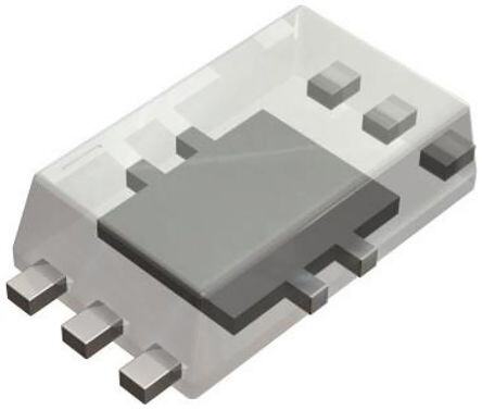
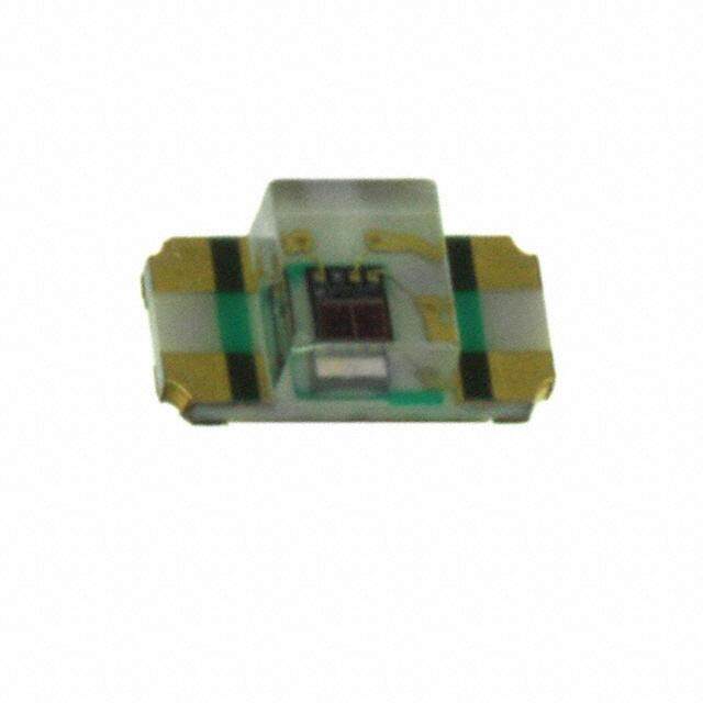
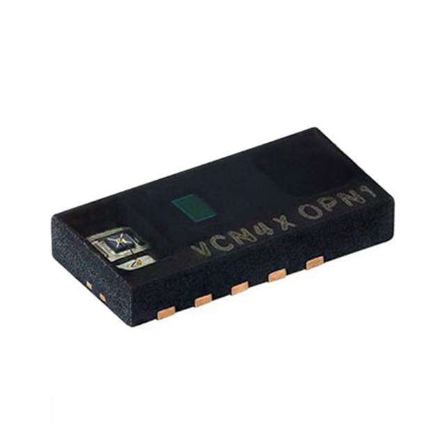
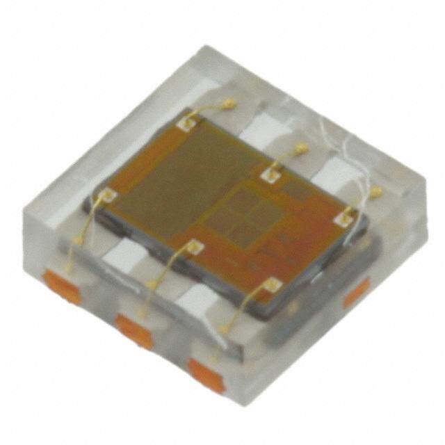
| 产品图片 |
|
| rohs | 符合RoHS无铅 / 符合限制有害物质指令(RoHS)规范要求 |
| 产品系列 | 环境光传感器,ROHM Semiconductor BH1750FVI-TR- |
| 数据手册 | |
| 产品型号 | BH1750FVI-TR |
| 产品 | Ambient Light Sensors |
| 产品种类 | 环境光传感器 |
| 供应商器件封装 | 6-WSOF |
| 其它名称 | BH1750FVI-TR-ND |
| 功率耗散 | 260 mW |
| 包装 | 带卷 (TR) |
| 商标 | ROHM Semiconductor |
| 安装类型 | 表面贴装 |
| 安装风格 | SMD/SMT |
| 封装 | Reel |
| 封装/外壳 | 6-SMD,扁平引线裸焊盘 |
| 封装/箱体 | WSOF-6I |
| 峰值波长 | 560 nm |
| 工作温度 | -40°C ~ 85°C |
| 工作电源电压 | 2.4 V to 3.6 V |
| 工厂包装数量 | 3000 |
| 带接近传感器 | 无 |
| 最大工作温度 | + 85 C |
| 最小工作温度 | - 40 C |
| 标准包装 | 3,000 |
| 波长 | 560nm |
| 特色产品 | http://www.digikey.com/product-highlights/cn/zh/rohm-ambient/2058 |
| 电压-电源 | 2.4 V ~ 3.6 V |
| 类型 | 环境 |
| 输出类型 | I²C |


- 商务部:美国ITC正式对集成电路等产品启动337调查
- 曝三星4nm工艺存在良率问题 高通将骁龙8 Gen1或转产台积电
- 太阳诱电将投资9.5亿元在常州建新厂生产MLCC 预计2023年完工
- 英特尔发布欧洲新工厂建设计划 深化IDM 2.0 战略
- 台积电先进制程称霸业界 有大客户加持明年业绩稳了
- 达到5530亿美元!SIA预计今年全球半导体销售额将创下新高
- 英特尔拟将自动驾驶子公司Mobileye上市 估值或超500亿美元
- 三星加码芯片和SET,合并消费电子和移动部门,撤换高东真等 CEO
- 三星电子宣布重大人事变动 还合并消费电子和移动部门
- 海关总署:前11个月进口集成电路产品价值2.52万亿元 增长14.8%


PDF Datasheet 数据手册内容提取
Ambient Light Sensor IC Series Digital 16bit Serial Output Type Ambient Light Sensor IC BH1750FVI No.11046EDT01 ●Descriptions BH1750FVI is an digital Ambient Light Sensor IC for I2C bus interface. This IC is the most suitable to obtain the ambient light data for adjusting LCD and Keypad backlight power of Mobile phone. It is possible to detect wide range at High resolution. ( 1 - 65535 lx ). ●Features 1) I2C bus Interface ( f / s Mode Support ) 2) Spectral responsibility is approximately human eye response 3) Illuminance to Digital Converter 4) Wide range and High resolution. ( 1 - 65535 lx ) 5) Low Current by power down function 6) 50Hz / 60Hz Light noise reject-function 7) 1.8V Logic input interface 8) No need any external parts 9) Light source dependency is little. ( ex. Incandescent Lamp. Fluorescent Lamp. Halogen Lamp. White LED. Sun Light ) 10) It is possible to select 2 type of I2C slave-address. 11) Adjustable measurement result for influence of optical window ( It is possible to detect min. 0.11 lx, max. 100000 lx by using this function. ) 12) Small measurement variation (+/- 20%) 13) The influence of infrared is very small. ●Applications Mobile phone, LCD TV, NOTE PC, Portable game machine, Digital camera, Digital video camera, PDA, LCD display ●Absolute Maximum Ratings Parameter Symbol Ratings Units Supply Voltage Vmax 4.5 V Operating Temperature Topr -40~85 ℃ Storage Temperature Tstg -40~100 ℃ SDA Sink Current Imax 7 mA Power Dissipation Pd 260※ mW ※ 70mm × 70mm × 1.6mm glass epoxy board. Derating in done at 3.47mW/℃ for operating above Ta=25℃. ●Operating Conditions Ratings Parameter Symbol Units Min. Typ. Max. VCC Voltage Vcc 2.4 3.0 3.6 V I2C Reference Voltage VDVI 1.65 - VCC V www.rohm.com 1/17 2011.11 - Rev.D © 2011 ROHM Co., Ltd. All rights reserved.
BH1750FVI Technical Note ●Electrical Characteristics ( VCC = 3.0V, DVI = 3.0V, Ta = 25℃, unless otherwise noted ) Limits Parameter Symbol Units Conditions Min. Typ. Max. Supply Current Icc1 - 120 190 µA Ev = 100 lx ※1 Powerdown Current Icc2 - 0.01 1.0 µA No input Light Peak Wave Length λp - 560 - nm Sensor out / Actual lx Measurement Accuracy S/A 0.96 1.2 1.44 times EV = 1000 lx ※1, ※2 Dark ( 0 lx ) Sensor out S0 0 0 3 count H-Resolution Mode ※3 H-Resolution Mode Resolution rHR - 1 - lx L-Resolution Mode Resolution rLR - 4 - lx H-Resolution Mode tHR - 120 180 ms Measurement Time L-Resolution Mode tLR - 16 24 ms Measurement Time Incandescent / rIF - 1 - times EV = 1000 lx Fluorescent Sensor out ratio ADDR Input ‘H’ Voltage VAH 0.7 * VCC - - V ADDR Input ‘L’ Voltage VAL - - 0.3 * VCC V DVI Input ‘L’ Voltage VDVL - - 0.4 V SCL, SDA Input ‘H’ Voltage 1 VIH1 0.7 * DVI - - V DVI ≧ 1.8V SCL, SDA Input ‘H’ Voltage 2 VIH2 1.26 - - V 1.65V ≦ DVI <1.8V SCL, SDA Input ‘L’ Voltage 1 VIL1 - - 0.3 * DVI V DVI ≧ 1.8V SCL, SDA Input ‘L’ Voltage 2 VIL2 - - DVI – 1.26 V 1.65V ≦ DVI < 1.8V SCL, SDA, ADDR IIH - - 10 µA Input ‘H’ Current SCL, SDA, ADDR IIL - - 10 µA Input ‘L’ Current I2C SCL Clock Frequency fSCL - - 400 kHz I2C Bus Free Time tBUF 1.3 - - µs I2C Hold Time ( repeated ) tHDSTA 0.6 - - µs START Condition I2C Set up time tSUSTA 0.6 - - µs for a Repeated START Condition I2C Set up time tSUSTD 0.6 - - µs for a Repeated STOP Condition I2C Data Hold Time tHDDAT 0 - 0.9 µs I2C Data Setup Time tSUDAT 100 - - ns I2C ‘L’ Period of the SCL Clock tLOW 1.3 - - µs I2C ‘H’ Period of the SCL Clock tHIGH 0.6 - - µs I2C SDA Output ‘L’ Voltage VOL 0 - 0.4 V IOL = 3 mA ※1 White LED is used as optical source. ※2 Measurement Accuracy typical value is possible to change '1' by "Measurement result adjustment function". ※3 Use H-resolution mode or H-resolution mode2 if dark data ( less than 10 lx ) is need. www.rohm.com 2/17 2011.11 - Rev.D © 2011 ROHM Co., Ltd. All rights reserved.
BH1750FVI Technical Note ●Reference Data 1.2 64 100000 56 1 10000 48 Ratio000...468 Measurement Result 12346420 HH-R-Reess. . L-Res. Measurement Result1010000 10 0.2 8 L-Res. 0 1 0 0 8 16 24 32 40 48 56 64 1 10 100 1000 10000 100000 400 500 600 Wa7v0e0length 8[0 n0m ] 900 1000 1100 Illuminance [ lx ] Illuminance [ lx ] Fig.1 Spectral Response Fig.2 Illuminance - Fig.3 Illuminance - Measure ment Result 1 Measuremnet Result 2 1.2 1.2 10 1 1 8 蛍光灯白熱灯感度比 1pin 0.8 ult s Ratio00..68 - + Ratio 0.6 - 1 pin ement Re 6 0.4 - ur 4 0.4 - + Meas 0.2 + 2 0.2 + H-Res. 0 0 -90 -60 -30 0 30 60 90 0 -90 -60 -30 0 30 60 90 Angle [ deg ] -40 -20 0 20 40 60 80 100 Angle [ deg ] Ta [ ℃ ] Fig.4 Directional Characteristics 1 Fig.5 Directional Characteristics 2 Fig.6 Dark Response 1.2 200 Fluorescent Light 1 IncanLdigehstcent ent150 0.8 m Ratio 0.6 KriptHoanL liogLghigethnt @ Measure100 0.4 Artifical Sun CC 50 Light I 0.2 White LED 0 0 -40 -20 0 20 40 60 80 100 0 0.5 1 1.5 2 2 2.5 3 3.5 4 Ta [ ℃ ] Ratio VCC [ V ] Fig.7 Measurement Accuracy Fig.8 Light Source Dependency Fig.9 VCC - ICC Temperature Dependency ( Fluorescent Light is set to '1' ) ( During measurement ) 10 1.2 1.2 OWN [ uA ] 1 0.81 DVI=1.8V 0.81 VCC=3V D WER Ratio 0.6 Ratio 0.6 O @ P 0.1 0.4 0.4 C IC 0.2 0.2 0.01 0 0 -40 -20 0 T20a [ ℃4 0] 60 80 100 2 2.5 VCC3 [ V ] 3.5 4 1.5 2 DVI2 . 5[ V ] 3 3.5 Fig.10 VCC – ICC@0 Lx Fig.11 Measurement Result Fig.12 Measurement Result ( POWER DOWN ) VCC Dependency DVI Dependency www.rohm.com 3/17 2011.11 - Rev.D © 2011 ROHM Co., Ltd. All rights reserved.
BH1750FVI Technical Note ●Block Diagram VCC DVI Logic SCL AMP ADC + I2C Interface SDA PD OSC GND ADDR ●Block Diagram Descriptions ・PD Photo diode with approximately human eye response. ・AMP Integration-OPAMP for converting from PD current to Voltage. ・ADC AD converter for obtainment Digital 16bit data. ・Logic + I2C Interface Ambient Light Calculation and I2C BUS Interface. It is including below register. Data Register → This is for registration of Ambient Light Data. Initial Value is "0000_0000_0000_0000". Measurement Time Register → This is for registration of measurement time. Initial Value is "0100_0101". ・OSC Internal Oscillator ( typ. 320kHz ). It is CLK for internal logic. ●Measurement Procedure Power supply Initial state is Power Down mode after State is automatically changed to VCC and DVI supply. Power Down mode. Power Down Power On Measurement Command One Time Measurement Continuous Measurement State Transition by I2C write-command. Automatically State Transition * "Power On" Command is possible to omit. www.rohm.com 4/17 2011.11 - Rev.D © 2011 ROHM Co., Ltd. All rights reserved.
BH1750FVI Technical Note ●Instruction Set Architecture Instruction Opecode Comments No active state. Power Down 0000_0000 Waiting for measurement command. Power On 0000_0001 Reset Data register value. Reset command is not acceptable in Reset 0000_0111 Power Down mode. Start measurement at 1lx resolution. Continuously H-Resolution Mode 0001_0000 Measurement Time is typically 120ms. Start measurement at 0.5lx resolution. Continuously H-Resolution Mode2 0001_0001 Measurement Time is typically 120ms. Start measurement at 4lx resolution. Continuously L-Resolution Mode 0001_0011 Measurement Time is typically 16ms. Start measurement at 1lx resolution. One Time H-Resolution Mode 0010_0000 Measurement Time is typically 120ms. It is automatically set to Power Down mode after measurement. Start measurement at 0.5lx resolution. One Time H-Resolution Mode2 0010_0001 Measurement Time is typically 120ms. It is automatically set to Power Down mode after measurement. Start measurement at 4lx resolution. One Time L-Resolution Mode 0010_0011 Measurement Time is typically 16ms. It is automatically set to Power Down mode after measurement. Change Measurement time Change measurement time. 01000_MT[7,6,5] ( High bit ) ※ Please refer "adjust measurement result for influence of optical window." Change Masurement time Change measurement time. 011_MT[4,3,2,1,0] ( Low bit ) ※ Please refer "adjust measurement result for influence of optical window." ※ Don't input the other opecode. ●Measurement mode explanation Measurement Mode Measurement Time. Resolurtion H-resolution Mode2 Typ. 120ms. 0.5 lx H-Resolution Mode Typ. 120ms. 1 lx. L-Resolution Mode Typ. 16ms. 4 lx. We recommend to use H-Resolution Mode. Measurement time ( integration time ) of H-Resolution Mode is so long that some kind of noise( including in 50Hz / 60Hz noise ) is rejected. And H-Resolution Mode is 1 l x resolution so that it is suitable for darkness ( less than 10 lx ) H-resolution mode2 is also suitable to detect for darkness. ●Explanation of Asynchronous reset and Reset command "0000_0111" 1) Asynchronous reset All registers are reset. It is necessary on power supply sequence. Please refer "Timing chart for VCC and DVI power supply sequence" in this page. It is power down mode during DVI = 'L'. 2) Reset command Reset command is for only reset Illuminance data register. ( reset value is '0' ) It is not necessary even power supply sequence.It is used for removing previous measurement result. This command is not working in power down mode, so that please set the power on mode before input this command. www.rohm.com 5/17 2011.11 - Rev.D © 2011 ROHM Co., Ltd. All rights reserved.
BH1750FVI Technical Note ●Timing chart for VCC and DVI power supply sequence DVI is I2C bus reference voltage terminal. And it is also asynchronous reset terminal. It is necessary to set to 'L' after VCC is supplied. In DVI 'L' term, internal state is set to Power Down mode. 1) Recommended Timing chart1 for VCC and DVI supply. VCC DVI Reset Term ( more than 1us ) 2) Timing chart2 for VCC and DVI supply. ( If DVI rises within 1µs after VCC supply ) VCC DVI Reset Term ( more than 1us ) Don't care state ADDR, SDA, SCL is not stable if DVI 'L' term ( 1us ) is not given by systems. In this case, please connect the resisters ( approximately 100kOhm ) to ADDR without directly connecting to VCC or GND, because it is 3 state buffer for Internal testing. www.rohm.com 6/17 2011.11 - Rev.D © 2011 ROHM Co., Ltd. All rights reserved.
BH1750FVI Technical Note ●Measurement sequence example from "Write instruction" to "Read measurement result" ex1) Continuously H-resolution mode ( ADDR = 'L' ) from Master to Slave from Slave to Master ① Send "Continuously H-resolution mode " instruction ST 0100011 0 Ack 00010000 Ack SP ② Wait to complete 1st H-resolution mode measurement.( max. 180ms. ) ③ Read measurement result. ST 0100011 1 Ack High Byte [ 15:8 ] Ack Low Byte [ 7:0 ] Ack SP How to calculate when the data High Byte is "10000011" and Low Byte is "10010000" ( 215 + 29 + 28 + 27 + 24 ) / 1.2 ≒ 28067 [ lx ] The result of continuously measurement mode is updated.( 120ms.typ at H-resolution mode, 16ms.typ at L-resolution mode ) ex2 ) One time L-resolution mode ( ADDR = 'H' ) ① Send "One time L-resolution mode " instruction ST 1011100 0 Ack 00100011 Ack SP ② Wait to complete L-resolution mode measurement.( max. 24ms. ) ③ Read measurement result ST 1011100 1 Ack High Byte [ 15:8 ] Ack Low Byte [ 7:0 ] Ack SP How to calculate when the data High Byte is "00000001" and Low Byte is "00010000" ( 28 + 24 ) / 1.2 ≒ 227 [ lx ] In one time measurement, Statement moves to power down mode after measurement completion.If updated result is need then please resend measurement instruction. www.rohm.com 7/17 2011.11 - Rev.D © 2011 ROHM Co., Ltd. All rights reserved.
BH1750FVI Technical Note ●Application circuit example of DVI terminal The DVI terminal is an asynchronous reset terminal. Please note that there is a possibility that IC doesn't operate normally if the reset section is not installed after the start-up of VCC. (Please refer to the paragraph of "Timing chart for VCC and DVI power supply sequence" ) The description concerning SDA and the terminal SCL is omitted in this application circuit example. Please design the application the standard of the I2C bus as it finishes being satisfactory. Moreover, the description concerning the terminal ADDR is omitted. Please refer to the paragraph of "Timing chart for VCC and DVI power supply sequence" about the terminal ADDR design. ex 1) The control signal line such as CPU is connected. BH1750FVI VCC SCL Micro 0.1µF Controller ADDR DVI 0.1µF GND SDA ex 2) Reset IC is used. 1, For Reset IC of the Push-Pull type BH1750FVI VCC SCL 0.1µF ADDR DVI 0.1µF RESET GND SDA Reset IC( Push-Pull type ) 2, For Reset IC of the Open drain output BH1750FVI 1kOhm VCC SCL 0.1µF ADDR DVI 0.1µF RESET GND SDA Reset IC( Open drain type ) ex 3) A different power supply is used. BH1750FVI VCC SCL 0.1µF V1 ADDR DVI GND SDA V2 0.1µF ※ Power supply of DVI must stand up later than power supply of VCC stand up, because it is necessary to secure reset section ( 1µs or more ). www.rohm.com 8/17 2011.11 - Rev.D © 2011 ROHM Co., Ltd. All rights reserved.
BH1750FVI Technical Note ex 4) LPF using CR is inserted between VCC and DVI. This method has the possibility that the Reset section of turning on the power supply can not satisfied. cannot be satisfied. Please design the set considering the characteristic of the power supply enough. R1 : 1kOhm BH1750FVI VCC SCL 0.1µF ADDR DVI C1 : 1µF GND SDA ◆ Notes when CR is inserted between VCC and DVI ※ Please note that there is a possibility that reset section ( 1µs ) can not be satisfied because the power supply is turned on when the rise time of VCC is slow ※ When VCC is turned off, the DVI voltage becomes higher than VCC voltage but IC destruction is not occred if recommended constant ( R1 = 1kOhm, C1 = 1µF ) is used. ※ Please note that there is a possibility that Reset section (1µsec) cannot be satisfied if wait time is not enough long after turning off VCC. (It is necessary to consider DVI voltage level after turning off VCC.) t1 t2 VCC DVI 2.4V 0.4V Reset Section : 1us or more 0V Please do the application design to secure Reset section 1us or more after the reclosing of the power supply. * ◆ Example of designing set when CR ( C = 1µF, R = 1kΩ ) is inserted between VCC and DVI with VCC=2.8V ①The rise time to 0→2.4V of VCC must use the power supply of 100µs or less. ②Please wait 25ms or more after VCC turn off ( VCC <= 0.05V ), because it is necessary to secure reset section ( 1µs or more ). Rise time of power supply : 100us or less Time to power supply reclosing : 25ms or more VCC れ 2.8V DVI 2.4V 0.4V 0.05V 0V Reset Section : 1us or more * Please do the application design to secure Reset section 1us or more after the reclosing of the power supply. www.rohm.com 9/17 2011.11 - Rev.D © 2011 ROHM Co., Ltd. All rights reserved.
BH1750FVI Technical Note ●I2C Bus Access 1 ) I2C Bus Interface Timing chart Write measurement command and Read measurement result are done by I2C Bus interface. Please refer the formally specification of I2C Bus interface, and follow the formally timing chart. SDA tf tr tSU ; DAT tf tHHD ;D STA tr t t BUF LOW SCL tHD ; STA tSU ; STA tSU;STO S tHD ; DAT tHtIGH Sr P S S S 2) Slave Address Slave Address is 2 types, it is determined by ADDR Terminal ADDR = ‘H’ ( ADDR ≧ 0.7VCC ) → “1011100“ ADDR = 'L' ( ADDR ≦ 0.3VCC ) → “0100011“ 3 ) Write Format BH1750FVI is not able to accept plural command without stop condition. Please insert SP every 1 Opecode. R/W ST Slave Address Ack Opecode Ack SP 0 4 ) Read Format R/W High Byte [15:8] ST Slave Address 1 Ack 215 214 213 212 211 210 29 28 Ack Low Byte [7:0] 27 26 25 24 23 22 21 20 Ack SP from Master to Slave from Slave to Master ex ) High Byte = "1000_0011" Low Byte = "1001_0000" ( 215 + 29 + 28 + 27 + 24 ) / 1.2 ≒ 28067 [ lx ] * I2C BUS is trademark of Phillips Semiconductors. Please refer formality specification. www.rohm.com 10/17 2011.11 - Rev.D © 2011 ROHM Co., Ltd. All rights reserved.
BH1750FVI Technical Note ●Adjust measurement result for influence of optical window. (sensor sensitivity adjusting ) BH1750FVI is possible to change sensor sensitivity. And it is possible to cancel the optical window influence (difference with / without optical window) by using this function. Adjust is done by changing measurement time. For example, when transmission rate of optical window is 50% (measurement result becomes 0.5 times if optical window is set), influence of optical window is ignored by changing sensor sensitivity from default to 2 times Sensor sensitivity is shift by changing the value of MTreg (measurement time register). MTreg value has to set 2 times if target of sensor sensitivity is 2 times. Measurement time is also set 2 times when MTreg value is changed from default to 2 times. ex) Procedure for changing target sensor sensitivity to 2 times. Please change Mtreg from ”0100_0101” ( default ) to ”1000_1010” ( default * 2 ). 1) Changing High bit of MTreg R/W ST Slave Address Ack 01000_100 Ack SP 0 2) Changing Low bit of MTreg R/W ST Slave Address Ack 011_01010 Ack SP 0 3) Input Measurement Command R/W ST Slave Address Ack 0001_0000 Ack SP 0 * This example is High Resolution mode, but it accepts the other measurement. 4) After about 240ms, measurement result is registered to Data Register. ( High Resolution mode is typically 120ms, but measurement time is set twice. ) The below table is seeing the changable range of MTreg. Min. Typ. Max. 0001_1111 0100_0101 1111_1110 binary changeable ( sensitivity : default * 0.45 ) default ( sensitivity : default * 3.68 ) range of MTreg 31 69 254 decimal ( sensitivity : default * 0.45 ) default ( sensitivity : default * 3.68 ) It is possilbe to detect 0.23lx by using this function at H-resolution mode. And it is possilbe to detect 0.11lx by using this function at H-resolution mode2. The below formula is to calculate illuminance per 1 count. H-reslution mode : Illuminance per 1 count ( lx / count ) = 1 / 1.2 *( 69 / X ) H-reslution mode2 : Illuminance per 1 count ( lx / count ) = 1 / 1.2 *( 69 / X ) / 2 1.2 : Measurement accuracy 69 : Default value of MTreg ( dec ) X : MTreg value The below table is seeing the detail of resolution. lx / count lx / count Mtregの値 at H-resolutin mode at H-resolution mode2 0001_1111 1.85 0.93 0100_0101 0.83 0.42 1111_1110 0.23 0.11 www.rohm.com 11/17 2011.11 - Rev.D © 2011 ROHM Co., Ltd. All rights reserved.
BH1750FVI Technical Note ●H-Resolution Mode2 H-resolution mode2 is 0.5lx ( typ. ) resolution mode. It is suitable if under less than 10 lx measure ment data is necessary. This measurement mode supports " Adjust measurement result for influence of optical window ". Please refer it. It is possible to detect min. 0.11 lx by using H-resolution mode2. ○ Instruction set architecture for H-resolution mode2 Instruction Opecode Comments Start measurement at 0.5lx resolution. Continuously H-Resolution Mode2 0001_0001 Measurement Time is typically 120ms. Start measurement at 0.5lx resolution. One Time H-Resolution Mode2 0010_0001 Measurement Time is typically 120ms. It is automatically set to Power Down mode after measurement. ○ Measurement sequence example from "Write instruction" to "Read measurement result" ex) Continuously H-resolution mode2 ( ADDR = 'L' ) from Master to Slave from Slave to Master ① Send "Continuously H-resolution mode2 " instruction ST 0100011 0 Ack 00010001 Ack SP ② Wait to complete 1st H-resolution mode2 measurement.( max. 180ms. ) ③ Read measurement result. High Byte [15:8] ST 0100011 1 Ack 214 213 212 211 210 29 28 27 Ack Low Byte [7:0] Ack SP 26 25 24 23 22 21 20 2-1 How to calculate when the data High Byte is "00000000" and Low Byte is "00010010" ( 23+ 20 ) / 1.2 ≒ 7.5 [ lx ] www.rohm.com 12/17 2011.11 - Rev.D © 2011 ROHM Co., Ltd. All rights reserved.
BH1750FVI Technical Note ●Terminal Description PIN No. Terminal Name Equivalent Circuit Function 1 VCC Power Supply Terminal I2C Slave-address Terminal VCC ADDR = ‘H’ ( ADDR ≧ 0.7VCC ) “1011100“ ADDR = 'L' ( ADDR ≦ 0.3VCC ) 2 ADDR “0100011“ ADDR Terminal is designed as 3 state buffer for internal test. So that please take care of VCC and DVI supply procedure.Please see P6. 3 GND GND Terminal 4 SDA I2C bus Interface SDA Terminal SDA, SCL Reference Voltage Terminal And DVI Terminal is also asynchronous 150kΩ Reset for internal registers.So that please set 5 DVI to 'L' ( at least 1µs, DVI <= 0.4V ) after VCC is supplied. BH1750FVI is pulled down by 150kOhm while DVI = 'L'. 6 SCL I2C bus Interface SCL Terminal ※These values are design-value, not guaranteed. www.rohm.com 13/17 2011.11 - Rev.D © 2011 ROHM Co., Ltd. All rights reserved.
BH1750FVI Technical Note ●Package Outlines Lot No. A A Product No. WSOF6I ( Unit : mm ) ●About an optical design on the device 0.8 mm 1.3 mm Min.0.4 mm Min.0.4 mm PD area ( 0.25 mm x 0.3 mm ) Please design the optical window so th at light can cover at least this are a. Min.0.4 mm Min.0.4 mm www.rohm.com 14/17 2011.11 - Rev.D © 2011 ROHM Co., Ltd. All rights reserved.
BH1750FVI Technical Note ●The method of distinguishing 1pin. There is some method of distinguishing 1pin. ① Distinguishing by 1Pin wide-lead ② Distinguishing by die pattern ③ Distinguishing by taper part of 1-3pin side ② (by die patern) is the easiest method to distinguish by naked eye. ② ③ A A Production code ① www.rohm.com 15/17 2011.11 - Rev.D © 2011 ROHM Co., Ltd. All rights reserved.
BH1750FVI Technical Note ●Cautions on use 1) Absolute Maximum Ratings An excess in the absolute maximum ratings, such as supply voltage ( Vmax ), temperature range of operating conditions ( Topr ), etc., can break down devices, thus making impossible to identify breaking mode such as a short circuit or an open circuit. If any special mode exceeding the absolute maximum ratings is assumed, consideration should be given to take physical safety measures including the use of fuses, etc. 2) GND voltage Make setting of the potential of the GND terminal so that it will be maintained at the minimum in any operating state. Furthermore, check to be sure no terminals are at a potential lower than the GND voltage including an actual electric transient. 3) Short circuit between terminals and erroneous mounting In order to mount ICs on a set PCB, pay thorough attention to the direction and offset of the ICs. Erroneous mounting can break down the ICs. Furthermore, if a short circuit occurs due to foreign matters entering between terminals or between the terminal and the power supply or the GND terminal, the ICs can break down. 4) Operation in strong electromagnetic field Be noted that using ICs in the strong electromagnetic field can malfunction them. 5) Inspection with set PCB On the inspection with the set PCB, if a capacitor is connected to a low-impedance IC terminal, the IC can suffer stress. Therefore, be sure to discharge from the set PCB by each process. Furthermore, in order to mount or dismount the set PCB to/from the jig for the inspection process, be sure to turn OFF the power supply and then mount the set PCB to the jig. After the completion of the inspection, be sure to turn OFF the power supply and then dismount it from the jig. In addition, for protection against static electricity, establish a ground for the assembly process and pay thorough attention to the transportation and the storage of the set PCB. 6) Input terminals In terms of the construction of IC, parasitic elements are inevitably formed in relation to potential. The operation of the parasitic element can cause interference with circuit operation, thus resulting in a malfunction and then breakdown of the input terminal. Therefore, pay thorough attention not to handle the input terminals; such as to apply to the input terminals a voltage lower than the GND respectively, so that any parasitic element will operate. Furthermore, do not apply a voltage to the input terminals when no power supply voltage is applied to the IC. In addition, even if the power supply voltage is applied, apply to the input terminals a voltage lower than the power supply voltage or within the guaranteed value of electrical characteristics. 7) Thermal design Perform thermal design in which there are adequate margins by taking into account the power dissipation ( Pd ) in actual states of use. 8) Treatment of package Dusts or scratch on the photo detector may affect the optical characteristics. Please handle it with care. 9) Rush current When power is first supplied to the CMOS IC, it is possible that the internal logic may be unstable and rush current may flow instantaneously. Therefore, give special consideration to power coupling capacitance, power wiring, width of GND wiring, and routing of connections. 10) The exposed central pad on the back side of the package There is an exposed central pad on the back side of the package. But please do it non connection. ( Don't solder, and don't do electrical connection ) Please mount by Footprint dimensions described in the Jisso Information for WSOF6I. This pad is GND level, therefore there is a possibility that LSI malfunctions and heavy-current is generated. www.rohm.com 16/17 2011.11 - Rev.D © 2011 ROHM Co., Ltd. All rights reserved.
BH1750FVI Technical Note ●Ordering part number B H 1 7 5 0 F V I - T R Part No. Part No. Package Packaging and forming specification FVI: WSOF6I TR: Embossed tape and reel WSOF6I <Tape and Reel information> 1.6±0.1 (MAX1.8 include BURR) Tape Embossed carrier tape 0.50.5 0.3 0.3 Quantity 3000pcs 6 5 4 4 5 6 TR R) Direction ±3.00.1±2.60.1MAX2.8 include BUR (0.45)(0.15) ((11..(1.5)42)) of feed (Treheel odnir ethcetio lenf tis h tahned 1 apnind oyfo pur opduull cot uist tah1te pt htianep uep opne rt hrieg hritg whth heann ydou hold ) ( 1 2 3 3 2 1 0.525 0.5 0.3 0.275 0.145±0.05 X MA S 0.0.7527±0.05 0.22±00.0.085S 0.08M Direction of feed (Unit : mm) Reel ∗ Order quantity needs to be multiple of the minimum quantity. www.rohm.com 17/17 2011.11 - Rev.D © 2011 ROHM Co., Ltd. All rights reserved.
DDaattaasshheeeett Notice Precaution on using ROHM Products 1. Our Products are designed and manufactured for application in ordinary electronic equipments (such as AV equipment, OA equipment, telecommunication equipment, home electronic appliances, amusement equipment, etc.). If you intend to use our Products in devices requiring extremely high reliability (such as medical equipment (Note 1), transport equipment, traffic equipment, aircraft/spacecraft, nuclear power controllers, fuel controllers, car equipment including car accessories, safety devices, etc.) and whose malfunction or failure may cause loss of human life, bodily injury or serious damage to property (“Specific Applications”), please consult with the ROHM sales representative in advance. Unless otherwise agreed in writing by ROHM in advance, ROHM shall not be in any way responsible or liable for any damages, expenses or losses incurred by you or third parties arising from the use of any ROHM’s Products for Specific Applications. (Note1) Medical Equipment Classification of the Specific Applications JAPAN USA EU CHINA CLASSⅢ CLASSⅡb CLASSⅢ CLASSⅢ CLASSⅣ CLASSⅢ 2. ROHM designs and manufactures its Products subject to strict quality control system. However, semiconductor products can fail or malfunction at a certain rate. Please be sure to implement, at your own responsibilities, adequate safety measures including but not limited to fail-safe design against the physical injury, damage to any property, which a failure or malfunction of our Products may cause. The following are examples of safety measures: [a] Installation of protection circuits or other protective devices to improve system safety [b] Installation of redundant circuits to reduce the impact of single or multiple circuit failure 3. Our Products are designed and manufactured for use under standard conditions and not under any special or extraordinary environments or conditions, as exemplified below. Accordingly, ROHM shall not be in any way responsible or liable for any damages, expenses or losses arising from the use of any ROHM’s Products under any special or extraordinary environments or conditions. If you intend to use our Products under any special or extraordinary environments or conditions (as exemplified below), your independent verification and confirmation of product performance, reliability, etc, prior to use, must be necessary: [a] Use of our Products in any types of liquid, including water, oils, chemicals, and organic solvents [b] Use of our Products outdoors or in places where the Products are exposed to direct sunlight or dust [c] Use of our Products in places where the Products are exposed to sea wind or corrosive gases, including Cl2, H2S, NH3, SO2, and NO2 [d] Use of our Products in places where the Products are exposed to static electricity or electromagnetic waves [e] Use of our Products in proximity to heat-producing components, plastic cords, or other flammable items [f] Sealing or coating our Products with resin or other coating materials [g] Use of our Products without cleaning residue of flux (even if you use no-clean type fluxes, cleaning residue of flux is recommended); or Washing our Products by using water or water-soluble cleaning agents for cleaning residue after soldering [h] Use of the Products in places subject to dew condensation 4. The Products are not subject to radiation-proof design. 5. Please verify and confirm characteristics of the final or mounted products in using the Products. 6. In particular, if a transient load (a large amount of load applied in a short period of time, such as pulse. is applied, confirmation of performance characteristics after on-board mounting is strongly recommended. Avoid applying power exceeding normal rated power; exceeding the power rating under steady-state loading condition may negatively affect product performance and reliability. 7. De-rate Power Dissipation (Pd) depending on Ambient temperature (Ta). When used in sealed area, confirm the actual ambient temperature. 8. Confirm that operation temperature is within the specified range described in the product specification. 9. ROHM shall not be in any way responsible or liable for failure induced under deviant condition from what is defined in this document. Precaution for Mounting / Circuit board design 1. When a highly active halogenous (chlorine, bromine, etc.) flux is used, the residue of flux may negatively affect product performance and reliability. 2. In principle, the reflow soldering method must be used; if flow soldering method is preferred, please consult with the ROHM representative in advance. For details, please refer to ROHM Mounting specification Notice - GE Rev.002 © 2014 ROHM Co., Ltd. All rights reserved.
DDaattaasshheeeett Precautions Regarding Application Examples and External Circuits 1. If change is made to the constant of an external circuit, please allow a sufficient margin considering variations of the characteristics of the Products and external components, including transient characteristics, as well as static characteristics. 2. You agree that application notes, reference designs, and associated data and information contained in this document are presented only as guidance for Products use. Therefore, in case you use such information, you are solely responsible for it and you must exercise your own independent verification and judgment in the use of such information contained in this document. ROHM shall not be in any way responsible or liable for any damages, expenses or losses incurred by you or third parties arising from the use of such information. Precaution for Electrostatic This Product is electrostatic sensitive product, which may be damaged due to electrostatic discharge. Please take proper caution in your manufacturing process and storage so that voltage exceeding the Products maximum rating will not be applied to Products. Please take special care under dry condition (e.g. Grounding of human body / equipment / solder iron, isolation from charged objects, setting of Ionizer, friction prevention and temperature / humidity control). Precaution for Storage / Transportation 1. Product performance and soldered connections may deteriorate if the Products are stored in the places where: [a] the Products are exposed to sea winds or corrosive gases, including Cl2, H2S, NH3, SO2, and NO2 [b] the temperature or humidity exceeds those recommended by ROHM [c] the Products are exposed to direct sunshine or condensation [d] the Products are exposed to high Electrostatic 2. Even under ROHM recommended storage condition, solderability of products out of recommended storage time period may be degraded. It is strongly recommended to confirm solderability before using Products of which storage time is exceeding the recommended storage time period. 3. Store / transport cartons in the correct direction, which is indicated on a carton with a symbol. Otherwise bent leads may occur due to excessive stress applied when dropping of a carton. 4. Use Products within the specified time after opening a humidity barrier bag. Baking is required before using Products of which storage time is exceeding the recommended storage time period. Precaution for Product Label QR code printed on ROHM Products label is for ROHM’s internal use only. Precaution for Disposition When disposing Products please dispose them properly using an authorized industry waste company. Precaution for Foreign Exchange and Foreign Trade act Since our Products might fall under controlled goods prescribed by the applicable foreign exchange and foreign trade act, please consult with ROHM representative in case of export. Precaution Regarding Intellectual Property Rights 1. All information and data including but not limited to application example contained in this document is for reference only. ROHM does not warrant that foregoing information or data will not infringe any intellectual property rights or any other rights of any third party regarding such information or data. ROHM shall not be in any way responsible or liable for infringement of any intellectual property rights or other damages arising from use of such information or data.: 2. No license, expressly or implied, is granted hereby under any intellectual property rights or other rights of ROHM or any third parties with respect to the information contained in this document. Other Precaution 1. This document may not be reprinted or reproduced, in whole or in part, without prior written consent of ROHM. 2. The Products may not be disassembled, converted, modified, reproduced or otherwise changed without prior written consent of ROHM. 3. In no event shall you use in any way whatsoever the Products and the related technical information contained in the Products or this document for any military purposes, including but not limited to, the development of mass-destruction weapons. 4. The proper names of companies or products described in this document are trademarks or registered trademarks of ROHM, its affiliated companies or third parties. Notice - GE Rev.002 © 2014 ROHM Co., Ltd. All rights reserved.
DDaattaasshheeeett General Precaution 1. Before you use our Products, you are requested to carefully read this document and fully understand its contents. ROHM shall not be in any way responsible or liable for failure, malfunction or accident arising from the use of a ny ROHM’s Products against warning, caution or note contained in this document. 2. All information contained in this document is current as of the issuing date and subj ect to change without any prior notice. Before purchasing or using ROHM’s Products, please confirm the latest information with a ROHM sale s representative. 3. The information contained in this document is provided on an “as is” basis and ROHM does not warrant that all information contained in this document is accurate an d/or error-free. ROHM shall not be in any way responsible or liable for any damages, expenses or losses incurred by you or third parties resulting from inaccuracy or errors of or concerning such information. Notice – WE Rev.001 © 2014 ROHM Co., Ltd. All rights reserved.
Mouser Electronics Authorized Distributor Click to View Pricing, Inventory, Delivery & Lifecycle Information: R OHM Semiconductor: BH1750FVI-TR