ICGOO在线商城 > 传感器,变送器 > 光学传感器 - 环境光,IR,UV 传感器 > BH1730FVC-TR

 Datasheet下载
- 型号: BH1730FVC-TR
- 制造商: ROHM Semiconductor
- 库位|库存: xxxx|xxxx
- 要求:
| 数量阶梯 | 香港交货 | 国内含税 |
| +xxxx | $xxxx | ¥xxxx |
查看当月历史价格
查看今年历史价格
BH1730FVC-TR产品简介:
ICGOO电子元器件商城为您提供BH1730FVC-TR由ROHM Semiconductor设计生产,在icgoo商城现货销售,并且可以通过原厂、代理商等渠道进行代购。 BH1730FVC-TR价格参考¥6.02-¥22.72。ROHM SemiconductorBH1730FVC-TR封装/规格:光学传感器 - 环境光,IR,UV 传感器, Optical Sensor Ambient 600nm I²C 6-SMD, Flat Lead Exposed Pad。您可以下载BH1730FVC-TR参考资料、Datasheet数据手册功能说明书,资料中有BH1730FVC-TR 详细功能的应用电路图电压和使用方法及教程。
BH1730FVC-TR是罗姆半导体(Rohm Semiconductor)推出的一款数字环境光传感器,属于光学传感器中的环境光、红外(IR)、紫外(UV)传感器类别。该传感器内置16位A/D转换器和I²C总线接口,具有高灵敏度和宽动态范围,可精确检测周围环境的光照强度。

主要应用场景包括:

1. 智能手机与平板电脑:用于自动调节屏幕亮度,提升视觉舒适度并降低功耗。
2. 笔记本电脑与显示器:根据环境光变化智能调整背光亮度,延长电池寿命。
3. 可穿戴设备:如智能手表、健康手环等,实现低功耗下的光线感知功能。
4. 智能家居设备:应用于智能照明系统,根据环境亮度自动开关或调光,提高能效。
5. 工业与楼宇自动化:用于光控开关、节能控制系统中,实现环境光监测。
6. 消费类电子产品:如电子书阅读器、数码相框等,优化显示效果。

BH1730FVC-TR采用小型化表面贴装封装(HLGA),适合空间受限的便携式设备。其高分辨率和良好的温度稳定性,使其在复杂光照环境下仍能保持精准测量。此外,该传感器具备抗干扰能力强、响应速度快等特点,适用于需要长时间稳定运行的场景。

综上,BH1730FVC-TR广泛应用于需自动光控调节的智能电子设备中,助力提升用户体验与能源效率。
| 参数 | 数值 |
| 产品目录 | |
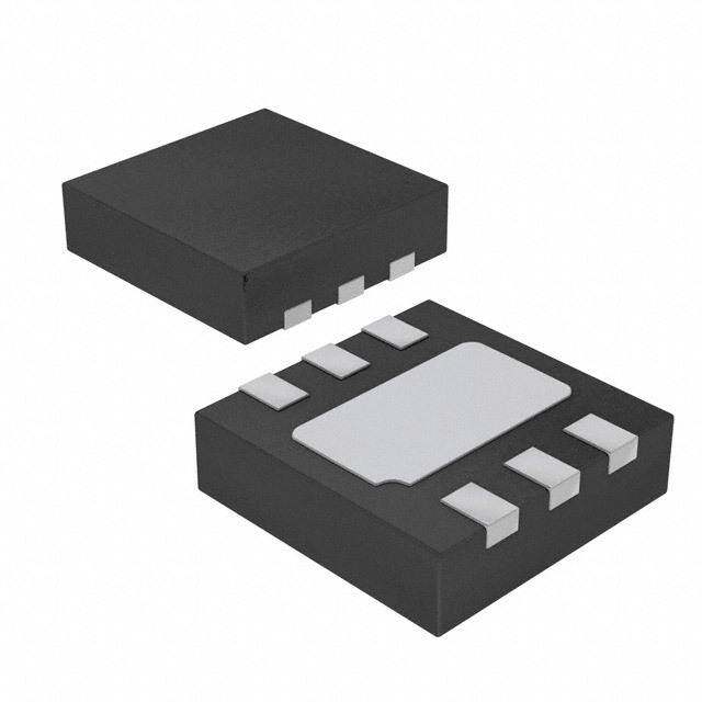
| 描述 | IC AMBIENT LIGHT SENSOR 6-WSOF环境光传感器 AMBIENT LIGHT SENSOR IC |
| 产品分类 | |
| 品牌 | Rohm Semiconductor |
| 产品手册 | |
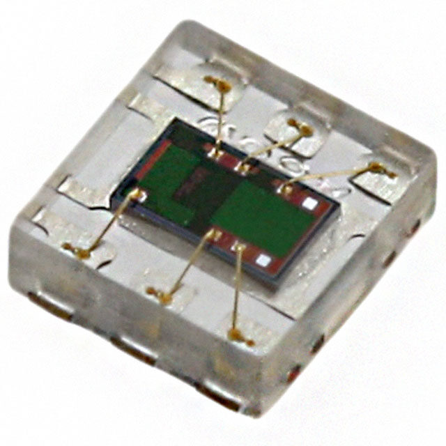
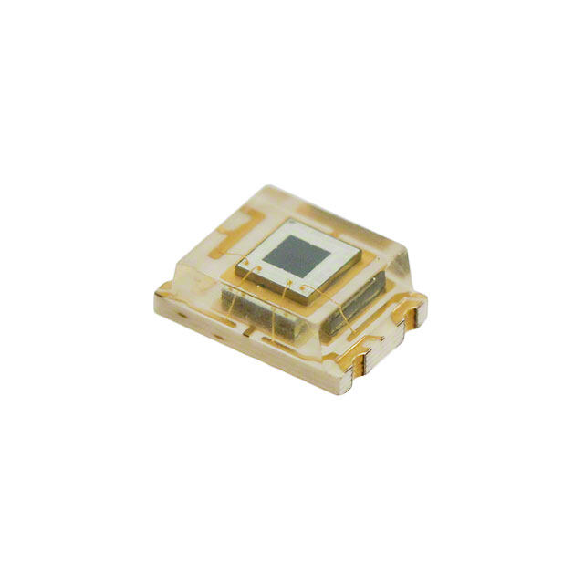
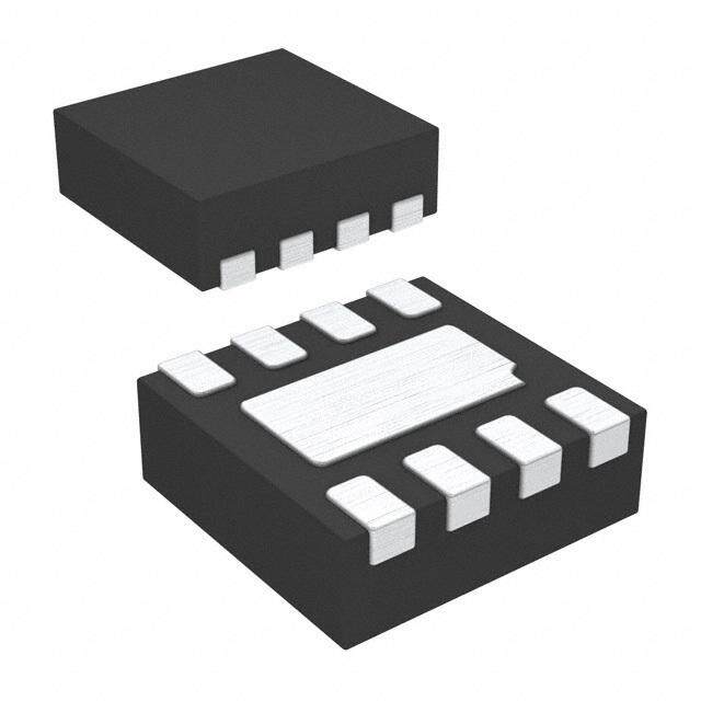
| 产品图片 |
|
| rohs | 符合RoHS无铅 / 符合限制有害物质指令(RoHS)规范要求 |
| 产品系列 | 环境光传感器,ROHM Semiconductor BH1730FVC-TR- |
| 数据手册 | |
| 产品型号 | BH1730FVC-TR |
| 产品 | Ambient Light Sensors |
| 产品种类 | 环境光传感器 |
| 供应商器件封装 | 6-WSOF |
| 其它名称 | BH1730FVCDKR |
| 功率耗散 | 260 mW |
| 包装 | Digi-Reel® |
| 商标 | ROHM Semiconductor |
| 安装类型 | 表面贴装 |
| 安装风格 | SMD/SMT |
| 封装 | Reel |
| 封装/外壳 | 6-SMD,扁平引线裸焊盘 |
| 封装/箱体 | WSOF-6 |
| 工作温度 | -40°C ~ 70°C |
| 工作电源电压 | 2.4 V to 3.6 V |
| 工厂包装数量 | 3000 |
| 带接近传感器 | 无 |
| 最大工作温度 | + 70 C |
| 最小工作温度 | - 40 C |
| 标准包装 | 1 |
| 波长 | 600nm |
| 电压-电源 | 2.4 V ~ 3.6 V |
| 类型 | 环境 |
| 输出类型 | I²C |


- 商务部:美国ITC正式对集成电路等产品启动337调查
- 曝三星4nm工艺存在良率问题 高通将骁龙8 Gen1或转产台积电
- 太阳诱电将投资9.5亿元在常州建新厂生产MLCC 预计2023年完工
- 英特尔发布欧洲新工厂建设计划 深化IDM 2.0 战略
- 台积电先进制程称霸业界 有大客户加持明年业绩稳了
- 达到5530亿美元!SIA预计今年全球半导体销售额将创下新高
- 英特尔拟将自动驾驶子公司Mobileye上市 估值或超500亿美元
- 三星加码芯片和SET,合并消费电子和移动部门,撤换高东真等 CEO
- 三星电子宣布重大人事变动 还合并消费电子和移动部门
- 海关总署:前11个月进口集成电路产品价值2.52万亿元 增长14.8%

PDF Datasheet 数据手册内容提取
Datasheet A mbient Light Sensor IC Series Digital 16bit Serial Output Type Ambient Light Sensor IC BH1730FVC General Description Key Specifications BH1730FVC is a digital Ambient Light Sensor IC with I2C ■ Supply Voltage Range: 2.4V to 3.6V bus interface. This IC is most suitable for obtaining ■ I2C I/O Voltage: 1.65V to V V CC ambient light data for adjusting LCD and backlight power ■ Detection Range: 0.001 lx to 100k lx of TV and mobile phone. It is capable of detecting a very ■ Current Consumption: 150 µA (Typ) wide range of illuminance. ■ Power Down Current: 0.85 µA (Typ) ■ Operating Temperature Range: -40°C to +85°C Features ■ I2C bus Interface Package W(Typ) x D(Typ) x H(Max) f/s Mode Support, Slave Address "0101001" WSOF6 1.60mm x 3.00mm x 0.75mm ■ 2 outputs with peak wavelengths of visible light and infrared light respectively. ■ Illuminance to digital converter ■ Low current by power down function ■ 50Hz / 60Hz light noise reject function ■ Light source dependency is small by the calculation using 2 outputs. (e.g. Incandescent lamp, Fluorescent lamp, Halogen lamp, White LED and Sun light) ■ Built-in interrupt function ■ Sensitivity adjustment function for compensation for illuminance decrease by optical window WSOF6 Applications LCD TV, Mobile Phone, Tablet PC, Note PC, Digital Camera, Portable Game Machine Typical Application Circuit 0.1uF 0.1uF VCC DVI V DVI AMP ADC ADC Logic SCL PD for visible light I2C Int+e rface SDA Mic ro + Controller INT Interface or AMP ADC Baseband INT Processor PD for infrared light OSC POR GND ○Product structure:Silicon monolithic integrated circuit. ○This product has no designed protection against radioactive rays. ○This product does not include laser transmitter. ○This product does not include optical load. ○This product includes Photo detector, ( Photo Diode ) inside of it. .w ww.rohm.com TSZ02201-0M3M0F616050-1-2 © 2012 ROHM Co., Ltd. All rights reserved. 1/20 TSZ22111・14・001 8.Jun.2016 Rev.001
BH1730FVC Pin Configuration TOP VIEW 1 VCC S C L 6 2 INT D V I 5 3 GND S D A 4 Pin Description Pin No. Pin Name Function 1 VCC Power supply terminal INT pin output terminal. 2 INT If not in use, connect to GND or leave it open. 3 GND GND terminal 4 SDA I2C bus interface SDA terminal 5 DVI I2C bus I/O voltage 6 SCL I2C bus interface SCL terminal Block Diagram VCC DVI AMP ADC ADC Logic SCL PD for visible light 2 + SDA IC Interface + INT Interface AMP ADC INT PD for infrared light OSC POR GND Description of Blocks 1. PD Photo diodes (PD) with peak wavelengths of visible light and infrared light respectively. 2. AMP Integrating AMP for converting PD current to voltage. 3. ADC Analog-to-Digital Converter for obtaining 16bit digital data. 4. ADC Logic + I2C Interface + INT Interface ADC control logic and I/F logic interface. 5. OSC Oscillator for clock of internal logic. 6. POR Power ON Reset. Please refer to "Power ON Sequence" on P14. www.rohm.com TSZ02201-0M3M0F616050-1-2 © 2012 ROHM Co., Ltd. All rights reserved. 2/20 TSZ22111・15・001 8.Jun.2016 Rev.001
BH1730FVC Absolute Maximum Ratings (Ta=25°C) Parameter Symbol Rating Unit Supply Voltage V 4.5 V CCMAX V , V , INT, SDA, DVI, SCL Terminal Voltage INTMAX SDAMAX -0.3 to +7 V V , V DVIMAX SCLMAX Operating Temperature Topr -40 to +85 °C Storage Temperature Tstg -40 to +100 °C SDA, INT Sink Current I 7 mA MAX Power Dissipation Pd 0.26 (Note 1) W (Note 1) 70mm x 70mm x 1.6mm glass epoxy board. Derating is at 3.47mW/°C for operating above Ta=25°C. Caution: Operating the IC over the absolute maximum ratings may damage the IC. The damage can either be a short circuit between pins or an open circuit between pins. Therefore, it is important to consider circuit protection measures, such as adding a fuse, in case the IC is operated over the absolute maximum ratings. Recommended Operating Conditions (Ta=-40℃ to +85℃) Parameter Symbol Min Typ Max Unit Supply Voltage V 2.4 3.0 3.6 V CC I2C I/O Voltage V 1.65 - V V DVI CC www.rohm.com TSZ02201-0M3M0F616050-1-2 © 2012 ROHM Co., Ltd. All rights reserved. 3/20 TSZ22111・15・001 8.Jun.2016 Rev.001
BH1730FVC Electrical Characteristics (V = 3.0V, V = 3.0V, Ta = 25°C, unless otherwise noted) CC DVI Parameter Symbol Min Typ Max Unit Conditions E = 100 lx (Note 1) V Supply Current ICC1 - 150 200 µA CONTROL register(00h) = "03h" and the other registers are default. No input Light Power Down Current ICC2 - 0.85 1.5 µA All registers are default. Peak Wave Length of Type0(Note 2) λp0 - 600 - nm Peak Wave Length of Type1(Note 2) λp1 - 840 - nm E = 1000 lx (Note 1) V ADC Count Value of Type0 D1k_0 1020 1200 1380 count TIMING register(01h) = "DAh" GAIN register(07h) = "00h" E = 1000 lx (Note 1) V ADC Count Value of Type1 D1k_1 153 180 207 count TIMING register(01h) = "DAh" GAIN register(07h) = "00h" No input Light Dark (0 lx) Sensor Out of Type0 S0_0 0 0 2 count TIMING register(01h) = "DAh" GAIN register(07h) = "00h" No input Light Dark (0 lx) Sensor Out of Type1 S0_1 0 0 2 count TIMING register(01h) = "DAh" GAIN register(07h) = “00h” Gain x1 Resolution of Type0 (Note 2) rG1 - 0.83 - lx/count TIMING register(01h) = "DAh"(Note 1) Gain x2 Resolution of Type0 (Note 2) rG2 - 0.42 - lx/count TIMING register(01h) = "DAh"(Note 1) Gain x64 Resolution of Type0 (Note 2) rG64 - 0.014 - lx/count TIMING register(01h) = "DAh"(Note 1) Gain x128 Resolution of Type0 (Note 2) rG128 - 0.007 - lx/count TIMING register(01h) = "DAh"(Note 1) Measurement Time Tmt1 - 104.6 150 ms TIMING register(01h) = "DAh" Internal Clock Period Tint - 2.8 4.0 µs INT Output 'L' Voltage VINT 0 - 0.4 V IINT = 3 mA SCL, SDA Input 'H' Voltage 1 VIH1 0.7*VDVI - - V VDVI ≥ 1.8V SCL, SDA Input 'H' Voltage 2 VIH2 1.26 - - V 1.65V ≤ VDVI <1.8V SCL, SDA Input 'L' Voltage 1 VIL1 - - 0.3*VDVI V VDVI ≥ 1.8V SCL, SDA Input 'L' Voltage 2 V - - V –1.26 V 1.65V ≤ V < 1.8V IL2 DVI DVI SCL, SDA, INT Input 'H' Current IIH - - 10 µA SCL, SDA, INT Input 'L' Current IIL - - 10 µA I2C SCL Clock Frequency fSCL - - 400 kHz I2C Bus Free Time t 1.3 - - µs BUF I2C Hold Time (Repeated) START t 0.6 - - µs Condition HDSTA I2C Setup Time for a Repeated START t 0.6 - - µs Condition SUSTA I2C Setup Time for STOP Condition t 0.6 - - µs SUSTO I2C Data Hold Time t 0 - 0.9 µs HDDAT I2C Data Setup Time tSUDAT 100 - - ns I2C 'L' Period of the SCL Clock tLOW 1.3 - - µs I2C 'H' Period of the SCL Clock tHIGH 0.6 - - µs I2C SDA Output 'L' Voltage V 0 - 0.4 V I = 3 mA OL OL (Note 1) White LED is used as optical source. (Note 2) Not 100% Tested www.rohm.com TSZ02201-0M3M0F616050-1-2 © 2012 ROHM Co., Ltd. All rights reserved. 4/20 TSZ22111・15・001 8.Jun.2016 Rev.001
BH1730FVC Typical Performance Curves 1.2 1.2 1. 01 11.0. 10 0.8 0.8 atio atio 0.6 Ratio atio 0.6 RR R 0.4 0.4 0.2 0.2 0 .00 00.. 000 400 500 600 700 800 900 1000 1100 400 500 600 700 800 900 1000 1100 Wavelength [ nm ] Wavelength [nm] WWavaveelelennggtthh [ [nnmm ]] Figure 1. Ratio vs Wavelength Figure 2. Ratio vs Wavelength (Spectral Response of Type0, Visible Light Peak) (Spectral Response of Type1, Infrared Light Peak) www.rohm.com TSZ02201-0M3M0F616050-1-2 © 2012 ROHM Co., Ltd. All rights reserved. 5/20 TSZ22111・15・001 8.Jun.2016 Rev.001
BH1730FVC Application Information 1. I2C Bus Access and Write / Read Format (1) I2C Bus Interface Timing Chart Write measurement command and Read measurement results are done by I2C Bus interface. Please refer to the formal specification of I2C Bus interface, and follow the formal timing chart. SDA tf tLOW tr tSU ; DAT tf tHD ; STA tr tBUF SCL tHD ; STA tSU ; STA tSU;STO tHD ; DAT tHIGH S Sr P S (2) Main Write Format (a) Write to Command Register Slave Address W Data to Command Register ST ACK ACK SP 0101001 0 1XXXXXXX (b) Write to Data Register Slave Address W Data specified at register address field ST ACK ACK 0101001 0 0XXXXXXX Data specified at register Data specified at register ACK ・・・ ACK ACK SP address field +1 address field +N Note:The register address that is set in the command register is used. (c) Write to Data Register After Write to Command Register Slave Address W Data to Command Register ST ACK ACK 0101001 0 1XXXXXXX Data specified at register Data specified at register ACK ・・・ ACK ACK SP address field address field +N (3) Main Read Format Slave Address R ST ACK Data specified at register address field ACK 0101001 1 Data specified at register Data specified at register ACK ・・・ ACK NACK SP address field +1 address field +N Note:The register address that is set in the command register is used. from Master to Slave from Slave to Master Note: BH1730FVC operates as I2C bus slave device. Note: Please refer to I2C bus specification of NXP semiconductor BH1730FVC continues to write or read data with address increments until master issues stop condition Address cycle: 00h -> 01h -> 02h -> 03h -> 04h -> 05h -> 06h -> 07h -> 12h -> 14h -> 15h -> 16h -> 17h www.rohm.com TSZ02201-0M3M0F616050-1-2 © 2012 ROHM Co., Ltd. All rights reserved. 6/20 TSZ22111・15・001 8.Jun.2016 Rev.001
BH1730FVC 2. Measurement Procedure Power Supply Initial state is power down mode after power supplied. Power Down POWER bit = H and ADC_EN bit =H Measurement State transits after measurement time(Tmt). Please refer to TIMING register on P9 about measurement time( Tmt ). Yes ONE_TIME bit = H? No INT_ STOP bit = H and Yes INT is active? No State Transition by I2C write-command. Automatic State Transition 3. Software Reset Command. All registers are reset and BH1730FVC becomes power down state by software reset command. www.rohm.com TSZ02201-0M3M0F616050-1-2 © 2012 ROHM Co., Ltd. All rights reserved. 7/20 TSZ22111・15・001 8.Jun.2016 Rev.001
BH1730FVC 4. Command Set Address Type Register name Register function [4:0] -- W COMMAND Specifies register address or sets special command 00h RW CONTROL Operation mode control 01h RW TIMING Light integration time control 02h RW INTERRUPT Interrupt function control 03h RW THLLOW Low byte of low interrupt threshold setting 04h RW THLHIGH High byte of low interrupt threshold setting 05h RW THHLOW Low byte of high interrupt threshold setting 06h RW THHHIGH High byte of high interrupt threshold setting 07h RW GAIN Gain control 12h R ID Part number and Revision ID 14h R DATA0LOW ADC Type0 low byte data register 15h R DATA0HIGH ADC Type0 high byte data register 16h R DATA1LOW ADC Type1 low byte data register 17h R DATA1HIGH ADC Type1 high byte data register (Note) Do not send command to the register which is not defined above. (1) COMMAND 7 6 5 4 3 2 1 0 CMD TRANSACTION ADDRESS / Special command default value 00h Field Bit Type Description CMD 7 W Write 1 00 : COMMAND<4:0> is ADDRESS field. 01 : Reserved. TRANSACTION 6 : 5 W 10 : Reserved. 11 : COMMAND<4:0> is Special command field. Specify register address. ADDRESS Don’t specify invalid register address. 4 : 0 W 00001 : Interrupt output reset. 00010 : Stop measurement in manual integration mode. Special command 00011 : Start measurement in manual integration mode. 00100 : Software reset Don’t input other commands. www.rohm.com TSZ02201-0M3M0F616050-1-2 © 2012 ROHM Co., Ltd. All rights reserved. 8/20 TSZ22111・15・001 8.Jun.2016 Rev.001
BH1730FVC (2) CONTROL (00h) 7 6 5 4 3 2 1 0 ADC_ ADC_ ONE_ DATA_ ADC_ RES POWER INTR VALID TIME SEL EN default value 00h Field Bit Type Description RES 7: 6 RW Write 00 0 : Interrupt is inactive. ADC_INTR 5 R 1 : Interrupt is active. 0 : ADC data is not updated after last reading. ADC_VALID 4 R 1 : ADC data is updated after last reading. 0 : ADC measurement is continuous. ONE_TIME 3 RW 1 : ADC measurement is one time. ADC transits to power down automatically. 0 : ADC measurement Type0 and Type1. DATA_SEL 2 RW 1 : ADC measurement Type0 only. 0 : ADC measurement stops. ADC_EN 1 RW 1 : ADC measurement starts. 0 : ADC power down. POWER 0 RW 1 : ADC power on. (3) TIMING (01h) 7 6 5 4 3 2 1 0 ITIME default value DAh Field Bit Type Description 00h : Start / Stop of measurement is set by special command. (ADC manual integration mode) 01h to FFh : Integration time is determined by ITIME value ITIME 7 : 0 RW Integration Time : ITIME_ms = Tint * 964 * (256 - ITIME) Measurement time : Tmt = ITIME_ms + Tint * 714 www.rohm.com TSZ02201-0M3M0F616050-1-2 © 2012 ROHM Co., Ltd. All rights reserved. 9/20 TSZ22111・15・001 8.Jun.2016 Rev.001
BH1730FVC (4) INTERRUPT (02h) 7 6 5 4 3 2 1 0 INT_ INT_ RES RES PERSIST STOP EN default value 00h Field Bit Type Description RES 7 RW Write 0 0 : ADC measurement does not stop. INT_STOP 6 RW 1 : ADC measurement stops and transits to power down mode when interrupt becomes active. RES 5 RW Write 0 0 : Disable interrupt function. INT_EN 4 RW 1 : Enable interrupt function. Interrupt persistence function. 0000 : Interrupt becomes active at each measurement end. 0001 : Interrupt status is updated at each measurement end. 0010 : Interrupt status is updated if two consecutive threshold PERSIST 3 : 0 RW judgments are the same. When set 0011 or more, interrupt status is updated if same threshold judgments continue consecutively same times as the number set in “PERSIST”. (5) TH_LOW (03h,04h) Register Address Bit Type Description TH lower LSBs 03h 7 : 0 RW Lower byte of low interrupt threshold TH lower MSBs 04h 7 : 0 RW Upper byte of low interrupt threshold default value 00h (6) TH_UP (05h,06h) Register Address Bit Type Description TH upper LSBs 05h 7 : 0 RW Lower byte of high interrupt threshold TH upper MSBs 06h 7 : 0 RW Upper byte of high interrupt threshold default value FFh (7) GAIN (07h) 7 6 5 4 3 2 1 0 RES GAIN default value 00h Field Bit Type Description RES 7 : 3 RW Write 00000 ADC resolution setting X00 : x1 gain mode GAIN 2 : 0 RW X01 : x2 gain mode X10 : x64 gain mode X11 : x128 gain mode www.rohm.com TSZ02201-0M3M0F616050-1-2 © 2012 ROHM Co., Ltd. All rights reserved. 10/20 TSZ22111・15・001 8.Jun.2016 Rev.001
BH1730FVC (8) PART_ID ( 12h ) 7 6 5 4 3 2 1 0 Part Number Revision ID default value 7Xh Field Bit Type Description Part number 7 : 4 R 0111 Revision ID 3 : 0 R Don’t use Revision ID Data (9) DATA0 (14h,15h) Register Address Bit Type Description DATA0 LSBs 14h 7 : 0 R Lower byte of ADC Type0 data DATA0 MSBs 15h 7 : 0 R Upper byte of ADC Type0 data default value 00h (10) DATA1 (16h,17h) Register Address Bit Type Description DATA1 LSBs 16h 7 : 0 R Lower byte of ADC Type1 data DATA1 MSBs 17h 7 : 0 R Upper byte of ADC Type1 data default value 00h www.rohm.com TSZ02201-0M3M0F616050-1-2 © 2012 ROHM Co., Ltd. All rights reserved. 11/20 TSZ22111・15・001 8.Jun.2016 Rev.001
BH1730FVC 5. Measurement Sequence Example from "Write start measurement command" to "Read measurement result" from Master to Slave from Slave to Master (1) Send "Continuous measurement mode" command. Slave Address W Write Command Register ST ACK ACK 0101001 0 1000_0000 Write CONTROL register ACK SP 0000_0011 (2) Wait measurement completion. (3) Read measurement result. Slave Address W Write Command Register ST ACK ACK SP 0101001 0 1001_0100 Slave Address R ST ACK Read DATA0 LSBs register ACK 0101001 1 Read DATA0 MSBs register ACK Read DATA1 LSBs register ACK Read DATA1 MSBs register NACK SP www.rohm.com TSZ02201-0M3M0F616050-1-2 © 2012 ROHM Co., Ltd. All rights reserved. 12/20 TSZ22111・15・001 8.Jun.2016 Rev.001
BH1730FVC 6. Lux Calculation using DATA0 and DATA1 BH1730FVC has two outputs, DATA0 (14h, 15h) for detecting mainly visible light, and DATA1 (16h, 17h) for detecting mainly infrared light. Lux value can be calculated by using these two outputs. The calculation formula depends on the characteristic of optical window. The example of the calculation is shown as below. Ex) No optical window or optical window that has flat transmittance from visible light to infrared light. if (DATA1/DATA0<0.26) Lx = ( 1.290 x DATA0 - 2.733 x DATA1 ) / Gain x 102.6 / ITIME_ms else if (DATA1/DATA0<0.55) Lx = ( 0.795 x DATA0 - 0.859 x DATA1 ) / Gain x 102.6 / ITIME_ms else if (DATA1/DATA0<1.09) Lx = ( 0.510 x DATA0 - 0.345 x DATA1 ) / Gain x 102.6 / ITIME_ms else if (DATA1/DATA0<2.13) Lx = ( 0.276 x DATA0 - 0.130 x DATA1 ) / Gain x 102.6 / ITIME_ms else Lx=0 ITIME_ms : Integration time of measurement (unit: ms). Please refer to TIMING register on P9. 7. Interrupt Function Interrupt function compares measurement result to preset interrupt threshold level. BH1730FVC uses two threshold levels (upper and lower). If measurement result is outside of the two thresholds, INT pin outputs 'L'. Interrupt threshold is set in Interrupt threshold registers (03h - 06h). Interrupt function is controlled by the Interrupt operational code. Interrupt persistence is set by PERSIST bit in INTERRUPT register(02h<3:0>). INT pin is an Nch open drain terminal. Hence this terminal has to have an external pull-up resistor to a voltage source. Maximum sink current rating of this terminal is 7mA. INT terminal state is high impedance when VCC is supplied. INT terminal becomes inactive by setting "Interrupt output reset" of special command. VCC current is consumed when INT terminal is 'L'. So it is recommended to reset INT terminal immediately when interrupt is detected. Master sends "Interrupt output reset" command. INT Terminal H persistence = 1 L H persistence = 2 L DATA0 Interrupt threshold H level sequential measurement results Interrupt threshold L level time www.rohm.com TSZ02201-0M3M0F616050-1-2 © 2012 ROHM Co., Ltd. All rights reserved. 13/20 TSZ22111・15・001 8.Jun.2016 Rev.001
BH1730FVC 8. Power On Sequence ALL registers of BH1730FVC are reset when VCC powers up. There are some notes about power up and down sequence as shown below. (1) Power ON Time: t 1 More than 2ms is needed to activate BH1730FVC after VCC becomes more than 2.4V from less than 0.4V. Operating voltage is from 2.4V to 3.6V. (2) Power OFF time: t 2 More than 1ms (VCC < 0.4V) is needed before supplying power to BH1730FVC. 2.4V VCC 0.4V t1 t2 t1 BH1730FVC Undefined Behavior active Undefined Behavior active Note: ”active state” means that BH1730FVC operates and accept I2C bus access correctly. 9. ALS Sensitivity Adjustment Function BH1730FVC is capable of changing its ALS sensitivity. This is used to compensate the effect of attenuation by the optical window. Adjustment is done by changing the integration time. For example, when transmission rate of optical window is 1/n (measurement result becomes 1/n times if optical window is above the sensor), the effect of optical window is compensated by changing integration time from default to n times. Take note that at 100,000 lx or higher illuminance cannot be measured even when the sensitivity is decreased. 10. Optical Design for the Device 0.8 mm 1.3 mm 0.4mm 0.4mm PD area (0.25mm x 0.3 mm) Please design the optical window so that light can cover at least this are. 0.4mm 0.4mm www.rohm.com TSZ02201-0M3M0F616050-1-2 © 2012 ROHM Co., Ltd. All rights reserved. 14/20 TSZ22111・15・001 8.Jun.2016 Rev.001
BH1730FVC I/O Equivalent Circuit PIN No. Terminal Name Equivalent Circuit 1 VCC 2 INT 3 GND DVI 4 SDA 5 DVI 150kΩ DVI 6 SCL (Note) These values are typical value. www.rohm.com TSZ02201-0M3M0F616050-1-2 © 2012 ROHM Co., Ltd. All rights reserved. 15/20 TSZ22111・15・001 8.Jun.2016 Rev.001
BH1730FVC Operational Notes 1. Reverse Connection of Power Supply Connecting the power supply in reverse polarity can damage the IC. Take precautions against reverse polarity when connecting the power supply, such as mounting an external diode between the power supply and the IC’s power supply pins. 2. Power Supply Lines Design the PCB layout pattern to provide low impedance supply lines. Furthermore, connect a capacitor to ground at all power supply pins. Consider the effect of temperature and aging on the capacitance value when using electrolytic capacitors. 3. Ground Voltage Ensure that no pins are at a voltage below that of the ground pin at any time, even during transient condition. 4. Ground Wiring Pattern When using both small-signal and large-current ground traces, the two ground traces should be routed separately but connected to a single ground at the reference point of the application board to avoid fluctuations in the small-signal ground caused by large currents. Also ensure that the ground traces of external components do not cause variations on the ground voltage. The ground lines must be as short and thick as possible to reduce line impedance. 5. Thermal Consideration Should by any chance the power dissipation rating be exceeded the rise in temperature of the chip may result in deterioration of the properties of the chip. In case of exceeding this absolute maximum rating, increase the board size and copper area to prevent exceeding the Pd rating. 6. Recommended Operating Conditions These conditions represent a range within which the expected characteristics of the IC can be approximately obtained. The electrical characteristics are guaranteed under the conditions of each parameter. 7. Inrush Current When power is first supplied to the IC, it is possible that the internal logic may be unstable and inrush current may flow instantaneously due to the internal powering sequence and delays, especially if the IC has more than one power supply. Therefore, give special consideration to power coupling capacitance, power wiring, width of ground wiring, and routing of connections. 8. Operation Under Strong Electromagnetic Field Operating the IC in the presence of a strong electromagnetic field may cause the IC to malfunction. 9. Testing on Application Boards When testing the IC on an application board, connecting a capacitor directly to a low-impedance output pin may subject the IC to stress. Always discharge capacitors completely after each process or step. The IC’s power supply should always be turned off completely before connecting or removing it from the test setup during the inspection process. To prevent damage from static discharge, ground the IC during assembly and use similar precautions during transport and storage. 10. Inter-pin Short and Mounting Errors Ensure that the direction and position are correct when mounting the IC on the PCB. Incorrect mounting may result in damaging the IC. Avoid nearby pins being shorted to each other especially to ground, power supply and output pin. Inter-pin shorts could be due to many reasons such as metal particles, water droplets (in very humid environment) and unintentional solder bridge deposited in between pins during assembly to name a few. 11. Unused Input Pins Input pins of an IC are often connected to the gate of a MOS transistor. The gate has extremely high impedance and extremely low capacitance. If left unconnected, the electric field from the outside can easily charge it. The small charge acquired in this way is enough to produce a significant effect on the conduction through the transistor and cause unexpected operation of the IC. So unless otherwise specified, unused input pins should be connected to the power supply or ground line. www.rohm.com TSZ02201-0M3M0F616050-1-2 © 2012 ROHM Co., Ltd. All rights reserved. 16/20 TSZ22111・15・001 8.Jun.2016 Rev.001
BH1730FVC Operational Notes – continued 12. Regarding the Input Pin of the IC This monolithic IC contains P+ isolation and P substrate layers between adjacent elements in order to keep them isolated. P-N junctions are formed at the intersection of the P layers with the N layers of other elements, creating a parasitic diode or transistor. For example (refer to figure below): When GND > Pin A and GND > Pin B, the P-N junction operates as a parasitic diode. When GND > Pin B, the P-N junction operates as a parasitic transistor. Parasitic diodes inevitably occur in the structure of the IC. The operation of parasitic diodes can result in mutual interference among circuits, operational faults, or physical damage. Therefore, conditions that cause these diodes to operate, such as applying a voltage lower than the GND voltage to an input pin (and thus to the P substrate) should be avoided. Resistor Transistor (NPN) Pin A Pin B B Pin B C Pin A E P+ P P+ P+ N P P+ B C N N N N Parasitic N N N E Elements Parasitic P Substrate P Substrate Elements GND GND GND GND Parasitic Parasitic N Region Elements Elements close-by Figure 3. Example of monolithic IC structure 13. Ceramic Capacitor When using a ceramic capacitor, determine the dielectric constant considering the change of capacitance with temperature and the decrease in nominal capacitance due to DC bias and others. 14. Area of Safe Operation (ASO) Operate the IC such that the output voltage, output current, and power dissipation are all within the Area of Safe Operation (ASO). www.rohm.com TSZ02201-0M3M0F616050-1-2 © 2012 ROHM Co., Ltd. All rights reserved. 17/20 TSZ22111・15・001 8.Jun.2016 Rev.001
BH1730FVC Ordering Information B H 1 7 3 0 F V C - T R Part Number Package Packaging and forming specification FVC: WSOF6 TR: Embossed tape and reel Marking Diagram and Methods of Distinguishing 1pin There are some methods to distinguish 1pin. ① Distinguishing by 1Pin marking ② Distinguishing by die pattern ③ Distinguishing by taper part of 1-3pin side ②(by die pattern) is the easiest method to distinguish by naked eye. ② LOT Number A H ③ Part Number Marking ① www.rohm.com TSZ02201-0M3M0F616050-1-2 © 2012 ROHM Co., Ltd. All rights reserved. 18/20 TSZ22111・15・001 8.Jun.2016 Rev.001
BH1730FVC Physical Dimension, Tape and Reel Information Package Name WSOF6 www.rohm.com TSZ02201-0M3M0F616050-1-2 © 2012 ROHM Co., Ltd. All rights reserved. 19/20 TSZ22111・15・001 8.Jun.2016 Rev.001
BH1730FVC Revision History Date Revision Changes 8. Jun. 2016 001 New release www.rohm.com TSZ02201-0M3M0F616050-1-2 © 2012 ROHM Co., Ltd. All rights reserved. 20/20 TSZ22111・15・001 8.Jun.2016 Rev.001
Notice Precaution on using ROHM Products 1. Our Products are designed and manufactured for application in ordinary electronic equipments (such as AV equipment, OA equipment, telecommunication equipment, home electronic appliances, amusement equipment, etc.). If you intend to use our Products in devices requiring extremely high reliability (such as medical equipment (Note 1), transport equipment, traffic equipment, aircraft/spacecraft, nuclear power controllers, fuel controllers, car equipment including car accessories, safety devices, etc.) and whose malfunction or failure may cause loss of human life, bodily injury or serious damage to property (“Specific Applications”), please consult with the ROHM sales representative in advance. Unless otherwise agreed in writing by ROHM in advance, ROHM shall not be in any way responsible or liable for any damages, expenses or losses incurred by you or third parties arising from the use of any ROHM’s Products for Specific Applications. (Note1) Medical Equipment Classification of the Specific Applications JAPAN USA EU CHINA CLASSⅢ CLASSⅡb CLASSⅢ CLASSⅢ CLASSⅣ CLASSⅢ 2. ROHM designs and manufactures its Products subject to strict quality control system. However, semiconductor products can fail or malfunction at a certain rate. Please be sure to implement, at your own responsibilities, adequate safety measures including but not limited to fail-safe design against the physical injury, damage to any property, which a failure or malfunction of our Products may cause. The following are examples of safety measures: [a] Installation of protection circuits or other protective devices to improve system safety [b] Installation of redundant circuits to reduce the impact of single or multiple circuit failure 3. Our Products are designed and manufactured for use under standard conditions and not under any special or extraordinary environments or conditions, as exemplified below. Accordingly, ROHM shall not be in any way responsible or liable for any damages, expenses or losses arising from the use of any ROHM’s Products under any special or extraordinary environments or conditions. If you intend to use our Products under any special or extraordinary environments or conditions (as exemplified below), your independent verification and confirmation of product performance, reliability, etc, prior to use, must be necessary: [a] Use of our Products in any types of liquid, including water, oils, chemicals, and organic solvents [b] Use of our Products outdoors or in places where the Products are exposed to direct sunlight or dust [c] Use of our Products in places where the Products are exposed to sea wind or corrosive gases, including Cl2, H2S, NH3, SO2, and NO2 [d] Use of our Products in places where the Products are exposed to static electricity or electromagnetic waves [e] Use of our Products in proximity to heat-producing components, plastic cords, or other flammable items [f] Sealing or coating our Products with resin or other coating materials [g] Use of our Products without cleaning residue of flux (even if you use no-clean type fluxes, cleaning residue of flux is recommended); or Washing our Products by using water or water-soluble cleaning agents for cleaning residue after soldering [h] Use of the Products in places subject to dew condensation 4. The Products are not subject to radiation-proof design. 5. Please verify and confirm characteristics of the final or mounted products in using the Products. 6. In particular, if a transient load (a large amount of load applied in a short period of time, such as pulse. is applied, confirmation of performance characteristics after on-board mounting is strongly recommended. Avoid applying power exceeding normal rated power; exceeding the power rating under steady-state loading condition may negatively affect product performance and reliability. 7. De-rate Power Dissipation depending on ambient temperature. When used in sealed area, confirm that it is the use in the range that does not exceed the maximum junction temperature. 8. Confirm that operation temperature is within the specified range described in the product specification. 9. ROHM shall not be in any way responsible or liable for failure induced under deviant condition from what is defined in this document. Precaution for Mounting / Circuit board design 1. When a highly active halogenous (chlorine, bromine, etc.) flux is used, the residue of flux may negatively affect product performance and reliability. 2. In principle, the reflow soldering method must be used on a surface-mount products, the flow soldering method must be used on a through hole mount products. If the flow soldering method is preferred on a surface-mount products, please consult with the ROHM representative in advance. For details, please refer to ROHM Mounting specification Notice-PGA-E Rev.003 © 2015 ROHM Co., Ltd. All rights reserved.
Precautions Regarding Application Examples and External Circuits 1. If change is made to the constant of an external circuit, please allow a sufficient margin considering variations of the characteristics of the Products and external components, including transient characteristics, as well as static characteristics. 2. You agree that application notes, reference designs, and associated data and information contained in this document are presented only as guidance for Products use. Therefore, in case you use such information, you are solely responsible for it and you must exercise your own independent verification and judgment in the use of such information contained in this document. ROHM shall not be in any way responsible or liable for any damages, expenses or losses incurred by you or third parties arising from the use of such information. Precaution for Electrostatic This Product is electrostatic sensitive product, which may be damaged due to electrostatic discharge. Please take proper caution in your manufacturing process and storage so that voltage exceeding the Products maximum rating will not be applied to Products. Please take special care under dry condition (e.g. Grounding of human body / equipment / solder iron, isolation from charged objects, setting of Ionizer, friction prevention and temperature / humidity control). Precaution for Storage / Transportation 1. Product performance and soldered connections may deteriorate if the Products are stored in the places where: [a] the Products are exposed to sea winds or corrosive gases, including Cl2, H2S, NH3, SO2, and NO2 [b] the temperature or humidity exceeds those recommended by ROHM [c] the Products are exposed to direct sunshine or condensation [d] the Products are exposed to high Electrostatic 2. Even under ROHM recommended storage condition, solderability of products out of recommended storage time period may be degraded. It is strongly recommended to confirm solderability before using Products of which storage time is exceeding the recommended storage time period. 3. Store / transport cartons in the correct direction, which is indicated on a carton with a symbol. Otherwise bent leads may occur due to excessive stress applied when dropping of a carton. 4. Use Products within the specified time after opening a humidity barrier bag. Baking is required before using Products of which storage time is exceeding the recommended storage time period. Precaution for Product Label A two-dimensional barcode printed on ROHM Products label is for ROHM’s internal use only. Precaution for Disposition When disposing Products please dispose them properly using an authorized industry waste company. Precaution for Foreign Exchange and Foreign Trade act Since concerned goods might be fallen under listed items of export control prescribed by Foreign exchange and Foreign trade act, please consult with ROHM in case of export. Precaution Regarding Intellectual Property Rights 1. All information and data including but not limited to application example contained in this document is for reference only. ROHM does not warrant that foregoing information or data will not infringe any intellectual property rights or any other rights of any third party regarding such information or data. 2. ROHM shall not have any obligations where the claims, actions or demands arising from the combination of the Products with other articles such as components, circuits, systems or external equipment (including software). 3. No license, expressly or implied, is granted hereby under any intellectual property rights or other rights of ROHM or any third parties with respect to the Products or the information contained in this document. Provided, however, that ROHM will not assert its intellectual property rights or other rights against you or your customers to the extent necessary to manufacture or sell products containing the Products, subject to the terms and conditions herein. Other Precaution 1. This document may not be reprinted or reproduced, in whole or in part, without prior written consent of ROHM. 2. The Products may not be disassembled, converted, modified, reproduced or otherwise changed without prior written consent of ROHM. 3. In no event shall you use in any way whatsoever the Products and the related technical information contained in the Products or this document for any military purposes, including but not limited to, the development of mass-destruction weapons. 4. The proper names of companies or products described in this document are trademarks or registered trademarks of ROHM, its affiliated companies or third parties. Notice-PGA-E Rev.003 © 2015 ROHM Co., Ltd. All rights reserved.
DDaattaasshheeeett General Precaution 1. Before you use our Products, you are requested to carefully read this document and fully understand its contents. ROHM shall not be in any way responsible or liable for failure, malfunction or accident arising from the use of a ny ROHM’s Products against warning, caution or note contained in this document. 2. All information contained in this document is current as of the issuing date and subj ect to change without any prior notice. Before purchasing or using ROHM’s Products, please confirm the latest information with a ROHM sale s representative. 3. The information contained in this document is provided on an “as is” basis and ROHM does not warrant that all information contained in this document is accurate an d/or error-free. ROHM shall not be in any way responsible or liable for any damages, expenses or losses incurred by you or third parties resulting from inaccuracy or errors of or concerning such information. Notice – WE Rev.001 © 2015 ROHM Co., Ltd. All rights reserved.
Mouser Electronics Authorized Distributor Click to View Pricing, Inventory, Delivery & Lifecycle Information: R OHM Semiconductor: BH1730FVC-TR