ICGOO在线商城 > 传感器,变送器 > 光学传感器 - 环境光,IR,UV 传感器 > APDS-9004-020
 Datasheet下载
- 型号: APDS-9004-020
- 制造商: Avago Technologies
- 库位|库存: xxxx|xxxx
- 要求:
| 数量阶梯 | 香港交货 | 国内含税 |
| +xxxx | $xxxx | ¥xxxx |
查看当月历史价格
查看今年历史价格
APDS-9004-020产品简介:
ICGOO电子元器件商城为您提供APDS-9004-020由Avago Technologies设计生产,在icgoo商城现货销售,并且可以通过原厂、代理商等渠道进行代购。 APDS-9004-020价格参考。Avago TechnologiesAPDS-9004-020封装/规格:光学传感器 - 环境光,IR,UV 传感器, Optical Sensor 环境 620nm 电流 1206(3216 公制)。您可以下载APDS-9004-020参考资料、Datasheet数据手册功能说明书,资料中有APDS-9004-020 详细功能的应用电路图电压和使用方法及教程。
型号为APDS-9004-020的光学传感器由Broadcom Limited生产,属于环境光、红外(IR)、紫外(UV)传感器类别。该传感器主要应用于需要检测环境光强度的电子设备中,例如:

1. 智能手机与平板电脑:用于自动调节屏幕亮度,提升用户体验并节省电能。
2. 笔记本电脑与显示器:实现背光自动调节功能,适应不同光照环境,保护用户视力。
3. 家电设备:如智能空调、智能灯具等,用于感知周围光照变化,实现自动化控制。
4. 汽车电子系统:应用于车内显示设备的背光调节或自动灯光控制系统。
5. 工业与楼宇自动化:用于照明控制系统,实现节能管理。

该传感器具备高灵敏度和宽动态范围,适合在多种光照条件下稳定工作,是一款性价比高且应用广泛的环境光传感器。
| 参数 | 数值 |
| 产品目录 | |
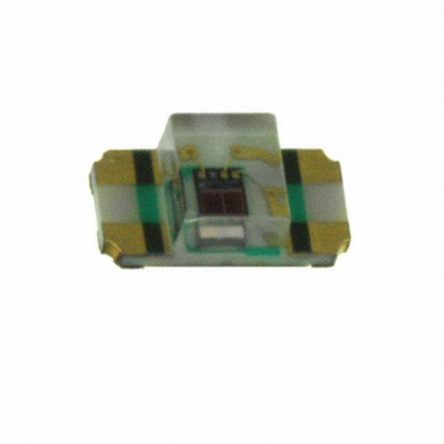
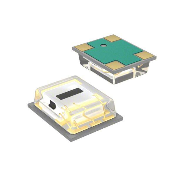
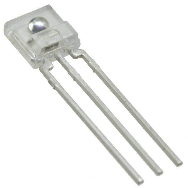
| 描述 | AMBIENT LIGHT SENSOR 4CHIPLED环境光传感器 Ambient Light sensor |
| 产品分类 | |
| 品牌 | Avago Technologies |
| 产品手册 | |
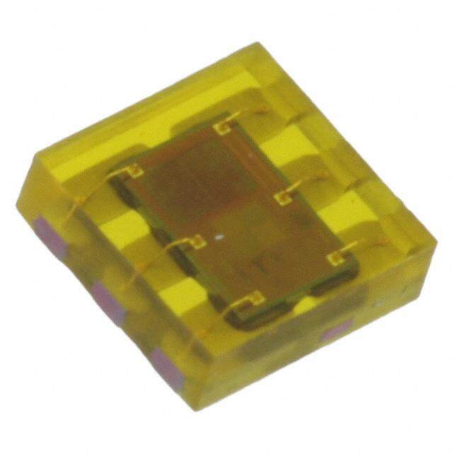
| 产品图片 |
|
| rohs | 符合RoHS无铅 / 符合限制有害物质指令(RoHS)规范要求 |
| 产品系列 | 环境光传感器,Avago Technologies APDS-9004-020- |
| 数据手册 | http://www.avagotech.com/docs/AV01-0184EN |
| 产品型号 | APDS-9004-020 |
| 上升时间 | 0.95 ms |
| 下降时间 | 0.8 ms |
| 产品 | Ambient Light Sensors |
| 产品目录绘图 |
|
| 产品目录页面 | |
| 产品种类 | 环境光传感器 |
| 供应商器件封装 | 4 引脚 ChipLED |
| 其它名称 | 516-1716-1 |
| 包装 | 剪切带 (CT) |
| 商标 | Avago Technologies |
| 安装类型 | 表面贴装 |
| 安装风格 | SMD/SMT |
| 封装 | Reel |
| 封装/外壳 | 1206(3216 公制) |
| 封装/箱体 | Chip LED-4 |
| 峰值波长 | 620 nm |
| 工作温度 | -40°C ~ 85°C |
| 工作电源电压 | 2.4 V to 5.5 V |
| 工厂包装数量 | 2500 |
| 带接近传感器 | 无 |
| 最大工作温度 | + 85 C |
| 最小工作温度 | - 40 C |
| 标准包装 | 1 |
| 波长 | 620nm |
| 电压-电源 | 2.4 V ~ 5.5 V |
| 类型 | Miniature SMD Ambient Light Photo Sensors |
| 输出类型 | 电流 |


- 商务部:美国ITC正式对集成电路等产品启动337调查
- 曝三星4nm工艺存在良率问题 高通将骁龙8 Gen1或转产台积电
- 太阳诱电将投资9.5亿元在常州建新厂生产MLCC 预计2023年完工
- 英特尔发布欧洲新工厂建设计划 深化IDM 2.0 战略
- 台积电先进制程称霸业界 有大客户加持明年业绩稳了
- 达到5530亿美元!SIA预计今年全球半导体销售额将创下新高
- 英特尔拟将自动驾驶子公司Mobileye上市 估值或超500亿美元
- 三星加码芯片和SET,合并消费电子和移动部门,撤换高东真等 CEO
- 三星电子宣布重大人事变动 还合并消费电子和移动部门
- 海关总署:前11个月进口集成电路产品价值2.52万亿元 增长14.8%

PDF Datasheet 数据手册内容提取
APDS-9004 Miniature Surface-Mount Ambient Light Photo Sensor Data Sheet Description Features The APDS-9004 is a low cost analog-output ambient • Spectral responsivity close to that of human eye light photo sensor in miniature chipLED lead-free, • ChipLED Reverse surface-mount package reverse surface mount package. It consists of a photo Height – 1.10mm sensor, whose spectral response is close to CIE standard Width – 3.20mm photopic observer. Hence, it provides an excellent responsivity that is close to the response of human Depth – 1.60mm eyes, as shown in Figure 2. It is suitable for portable • Good output linearity across wide illumination applications with its ultra small package design. range The APDS-9004 is ideal for applications in which the • Low sensitivity variation across various light measurement of ambient light is used to control sources display backlighting. Mobile appliances such as the mobile phones and PDAs that draw heavy current from • Operating temperature display backlighting will benefit from incorporating -40°C to 85°C these photo sensor products in their designs by • Vcc supply 2.4 to 5.5V reducing power consumption significantly. • Lead-free package, RoHS compliance. Applications • Detection of ambient light to control display backlighting - Mobile devices – Mobile phones, PDAs - Computing devices – Notebooks, Webpads - Consumer devices – TVs, Video Cameras, Digital Still Cameras • Automatic Residential and Commercial Lighting Management • Electronic Signs and Signals CAUTION: It is advised that normal static precautions be taken in handling and assembly of this component to prevent damage and/or degradation which may be induced by ESD.
Application Support Information The Application Engineering Group is available to assist you with the application design associated with APDS- 9004 ambient light photo sensor module. You can contact them through your local sales representatives for additional details. Ordering Information Part Number Packaging Type Package Quantity APDS-9004-020 Tape and Reel 4-pins Chipled package 2500 Typical Application Circuit APDS-9004 Block Diagram Pin 3:V Pin 2:V CC CC APDS -9004 Pin 1:OUT R LOAD Pin 4:NC Figure 1. Typical application circuit for APDS-9004 Notes : PIN 2 and PIN 3 Vcc need to be externally shorted. Figure 2. Relative Spectral Response Vs. Wavelength Figure 1 Table Component Recommended Application Relative Spectral Response Vs. Wavelength Circuit Component R 1k ohm Relative Spectral Response Vs Wavelength LOAD 1.2 Eye e s 1 n APDS-9004 o p I/O Pins Configuration Table s Re 0.8 al Pin Symbol Description r t c 0.6 e 1 OUT OUT p S e 2 VCC VCC v 0.4 ti a 3 VCC VCC el R 0.2 4 NC No Connect 0 350 550 750 950 1150 Wavelength (nm) 2
Absolute Maximum Ratings For implementations where case to ambient thermal resistance is ≤ 50 °C /W Parameter Symbol Min. Max. Units Storage Temperature T -40 85 °C S Operating Temperature T -40 85 °C A Supply Voltage V 0 6.0 V CC Recommended Operating Conditions Parameter Symbol Min. Max. Units Supply Voltage V 2.4 5.5 V CC Electrical & Optical Specifications (Ta=25°°°°°C) Parameter Symbol Min. Typ. Max. Units Conditions Output Current (I)[note4] I 3 19 31 uA Vcc=3.0V, Lux=10 _OUT1 [Note 2] Output Current (II)[note4] I 90 230 370 uA Vcc=3.0V, Lux=100 _OUT2 [Note 2] Output Current (III)[note4] I - 276 - uA Vcc=3.0V, Lux=100 _OUT3 [Note 1] Dark Current I - - 0.5 uA Vcc=5.0V,Lux=0 _DARK Light Current Ratio I / I - 1.2 - - _OUT3 _OUT2 Saturation Output Voltage V 2.2 2.32 - V Vcc=3.0V, Lux=100, O Rload=1M Peak Sensitivity Wavelength - 620 - nm Settling Time with pulsed Vcc Tset 3.5 ms Vcc pulse = 0V to 3V, Rload=1kΩ, Lux=100 [Note 3] Propagation Delay time Td - 600 - us Vcc=3.0V, Lux=100, Rload=1k Ω [Note 3] Storage Delay time Ts - 200 - us Vcc=3.0V, Lux=100, Rload=1k Ω [Note 3] Rise Time Tr - 0.95 ms Vcc=3.0V, Lux=100, Rload=1kΩ [Note 3] Fall Time Tf - 0.8 ms Vcc=3.0V, Lux=100, Rload=1kΩ[Note 3] Note: 1. Illuminance by Incandescent lamp 2. Fluorescent light is used as light source. White LED is substituted in mass production. 3. White LED is used as light source. 4. Other binning options are available. Please contact your Avago Technologies representative for information on current available bins 3
APDS-9004 Performance Charts Average Iout Vs Lux (Vcc=3V,T=25C) Relative Output Current Vs Temperature (Vcc=3V, 100 Lux) 10000 2.50 White LED 2.00 1000 uA) A) ut( ut( 1.50 o o e I 100 e I g v vera elati 1.00 A R 10 0.50 Relative Iout 0.00 1 -50 -25 0 25 50 75 100 10 100 1000 Temp(C) Lux Relative Output current Vs Vcc ( T=25C, 100 Lux) Relative Iout Vs Angle 1.10 1.20 1.08 Relative Iout 1.00 nt re1.06 e output cur11..0024 elative Iout 00..6800 elativ1.00 R 0.40 R 0.20 0.98 Relative output current 0.00 0.96 2 2.5 3 3.5 4 4.5 5 5.5 6 -90 -60 -30 0 30 60 90 Vcc(V) Angle 4
APDS-9004 Light Measurement Circuit and Waveforms I_pulse Pin 3:V CC Pin 2:V CC II__ppuullssee Pin 1:OUT VVOOUUTT APDS-9004 9900%% GGNNDD 1100%% R LOAD Pin 4:NC ttrr ttff ttdd ttss sensor-output attains ~95% of its voltage magnitude corresponds to the set light level VCC Pulse from PG Sensor Output at load Tset 5
APDS-9004 Package Outline 6
APDS-9004 Tape and Reel Dimensions 7
Moisture Proof Packaging Chart All APDS-9004 options are shipped in moisture proof package. Once opened, moisture absorption begins. This part is compliant to JEDEC Level 3. Baking conditions Recommended Storage Conditions If the parts are not stored in dry conditions, they must Storage Temperature 10°C to 30°C be baked before reflow to prevent damage to the parts. Relative Humidity Below 60% RH Package Temp. Time Time from Unsealing to Soldering In Reels 60°C 48 hours After removal from the bag, the parts should be In Bulk 100°C 6 hours soldered within seven days if stored at the recommended storage conditions. If times longer than Baking should only be done once. seven days are needed, the parts must be stored in a dry box. 8
Recommended Reflow Profile MAX 260°C 255 R3 R4 230 217 °E (C) 128000 R2 60 sec to 90 sec UR 150 Above 217 °C T A R5 ER 120 R1 P M E T 80 T - 25 0 50 100 150 200 250 300 P1 P2 P3 P4 t-TIME HEAT SOLDER PASTE DRY SOLDER COOL DOWN (SECONDS) UP REFLOW Process Zone Symbol T Maximum ∆T/ time or Duration Heat Up P1, R1 25°C to 150°C 3°C/s Solder Paste Dry P2, R2 150°C to 200°C 100s to 180s Solder Reflow P3, R3 200°C to 255°C 3°C/s P3, R4 255°C to 200°C -6°C/s Cool Down P4, R5 200°C to 25°C -6°C/s Time maintained above 217°C > 217°C 60s to 90s Peak Temperature 260°C Time within 5°C of actual Peak Temperature > 255°C 20s to 40s Time 25°C to Peak Temperature 25°C to 260°C 8mins The reflow profile is a straight-line representation of a The dwell time above the liquidus point of solder nominal temperature profile for a convective reflow should be between 20 and 40 seconds. It usually takes solder process. The temperature profile is divided into about 20 seconds to assure proper coalescing of the four process zones, each with different ∆T/∆time solder balls into liquid solder and the formation of good temperature change rates or duration. The ∆T/∆time solder connections. Beyond a dwell time of 40 seconds, rates or duration are detailed in the above table. The the intermetallic growth within the solder connections temperatures are measured at the component to becomes excessive, resulting in the formation of weak printed circuit board connections. and unreliable connections. The temperature is then rapidly reduced to a point below the solidus In process zone P1, the PC board and APDS-9004 pins temperature of the solder, usually 200°C (392°F), to are heated to a temperature of 150°C to activate the allow the solder within the connections to freeze solid. flux in the solder paste. The temperature ramp up rate, R1, is limited to 3°C per second to allow for even Process zone P4 is the cool down after solder freeze. heating of both the PC board and APDS-9004 pins. The cool down rate, R5, from the liquidus point of the solder to 25°C (77°F) should not exceed 6°C per second Process zone P2 should be of sufficient time duration maximum. This limitation is necessary to allow the PC (100 to 180 seconds) to dry the solder paste. The board and APDS-9004 pins to change dimensions temperature is raised to a level just below the liquidus evenly, putting minimal stresses on the APDS-9004. point of the solder, usually 200°C (392°F). It is recommended to perform reflow soldering no Process zone P3 is the solder reflow zone. In zone P3, more than twice. the temperature is quickly raised above the liquidus point of solder to 255°C (491°F) for optimum results. 9
Appendix A: SMT Assembly Application Note Solder Pad, Mask and Metal Metal Stencil Stencil For Solder Aperture Paste Printing Land Pattern Solder Mask PCBA Slot Opening for APDS- 9004 to be exposed on the Reverse Side of the PCBA Figure 1. Stencil and PCBA 1.1 Recommended Land Pattern Soldering C Terminal L 1.00 0.71 0.945 1.89 Slot Opening for APDS-9004 to be exposed on the Reverse Side of 0.71 the PCBA 0.50 0.60 0.60 Unit: mm 2.00 Tolerance: +/- 0.2 Figure 2. Recommended Land Pattern 10
1.2 Recommended Metal Solder Stencil Aperture It is recommended that a 0.11 mm (0.004 inches) thick stencil be used for solder paste printing. Aperture opening for shield pad is 0.6mm x 0.71mm. This is to ensure adequate printed solder paste volume and no shorting. Aperture Opening 0.11 Unit: mm 1.7 3.31 Figure 3. Solder stencil aperture 1.3 Adjacent Land Keepout and Solder Mask Areas Adjacent land keep-out is the maximum space occupied by the unit relative to the land pattern. There should be no other SMD components within this area. The minimum solder resist strip width required to avoid solder bridging adjacent pads is 0.2 mm. Note: Wet/Liquid Photo-Imageable solder resist/mask is recommended. 2.7 Mounting 4.31 Center Unit: mm 0.2 MIN. Figure 4. Adjacent land keepout and solder mask areas. 11
Appendix B: Optical Window Design for APDS-9004 Optical Window Dimensions To ensure that the performance of the APDS-9004 will cylindrical piece of transparent plastic, which makes not be affected by improper window design, there are use of total internal reflection to focus the light. some constraints on the dimensions and design of the The thickness of the window should be kept as window. There is a constraint on the minimum size of minimum as possible because there is a loss of power the window, which is placed in front of the photo light in every optical window of about 8% due to reflection sensor, so that it will not affect the angular response (4% on each side) and an additional loss of energy in of the APDS-9004. This minimum dimension that is the plastic material. recommended will ensure at least a ±35° light reception cone. Figure 5a and 5b illustrate the two types of window that we have recommended which could either be a If a smaller window is required, a light pipe or light flat window or a flat window with light pipe. guide can be used. A light pipe or light guide is a Flat APDS-9004 Figure 5(a). Window Size Determination for Flat Window Figure 5(b). Window Design of Flat Window with Light Guide D1 Top View T WD D2 D1 L Z APDS-9004 Light Receving Area Figure 6. Recommended Window Dimensions 12
Table 1 and Figure 6 below show the recommended dimensions of the window. These dimension values are based on a window thickness of 1.0mm with a refractive index 1.585. WD: Working Distance between window front panel & APDS-9004 D1: Window Diameter T: Thickness L: Length of Light Pipe D2: Light Pipe Diameter Z: Distance between window rear panel and APDS-9004 Table 1: Recommended dimension for optical window WD (T+L+Z) Flat Window Flat Window with Light Guide Z D1 D1 L 1.5 0.5 2.1 - - 2.0 1.0 2.8 - - 2.5 1.5 3.5 - - 3.0 2.0 4.2 2.5 1.5 ( All dimensions are in mm ) Note : Active area center to coincide with window center (flat or with light guide). The window should be placed directly on top of the photo sensor to achieve better performance and if a flat window with a light pipe is used, dimension D2 should be 1.5mm to optimize the performance of APDS-9004. 2.1 Optical Window Material The material of the window is recommended to be polycarbonate. The surface finish of the plastic should be smooth, without any texture. The recommended plastic material for use as a window is available from Bayer AG and Bayer Antwerp N. V. (Europe), Bayer Corp.(USA) and Bayer Polymers Co., Ltd. (Thailand), as shown in Table 2. Table 2: Recommended Plastic Materials Material number Visible light transmission Refractive index Makrolon LQ2647 87% 1.587 Makrolon LQ3147 87% 1.587 Makrolon LQ3187 85% 1.587 13
Appendix C: General Application Guide for APDS-9004 The APDS-9004 is a low cost analog-output ambient light photo sensor whose spectral response closely emulates the human eyes. APDS-9004 consists of a phototransistor that enables the photo sensor to produce a high gain photo current to a sufficient level that can be converted to voltage with a standard value of external resistor. APDS-9004 is then easily integrated into systems that use ADC input which is available for sampling of the external source, as shown in figure 7 below. The amount of converted voltage, Vout, is mainly dependant proportionally on the photo current which generated by the brightness of the light shone on the photo sensor and the load resistor used, RL. Increasing the brightness of the light or/and the load resistor will increase the output voltage. Brightness is measured as “LUX” unit, which describes how intense a light source that our eyes perceive. LUX meter is the equipment for “LUX” measurement. Light sources with the same LUX level appear at the same brightness to the human eyes. Vcc 2,3 Light Source 1 Vout APDS-9004 A/D 4 C RL micro- controller NC Figure 7. Configuration of APDS-9004 being used directly Selection of the load resistor RL will determine the amount of current-to-voltage conversion in the circuit. Light source e.g. fluorescent light consists of ac noise about 100Hz frequency. A capacitor of 10uF, which acting as a low-pass filter, is recommended to add in parallel with the load resistor to by-pass this ripples. For product information and a complete list of distributors, please go to our web site: www.avagotech.com Avago, Avago Technologies, and the A logo are trademarks of Avago Technologies, Limited in the United States and other countries. Data subject to change. Copyright © 2006 Avago Technologies Pte. All rights reserved. AV01-0184EN - September 14, 2006