ICGOO在线商城 > 传感器,变送器 > 光学传感器 - 环境光,IR,UV 传感器 > TSL237T
 Datasheet下载
- 型号: TSL237T
- 制造商: AUSTRIAMICROSYSTEMS
- 库位|库存: xxxx|xxxx
- 要求:
| 数量阶梯 | 香港交货 | 国内含税 |
| +xxxx | $xxxx | ¥xxxx |
查看当月历史价格
查看今年历史价格
TSL237T产品简介:
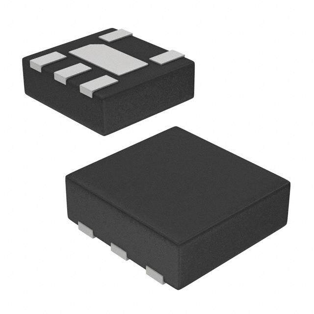
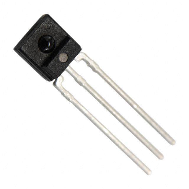
ICGOO电子元器件商城为您提供TSL237T由AUSTRIAMICROSYSTEMS设计生产,在icgoo商城现货销售,并且可以通过原厂、代理商等渠道进行代购。 TSL237T价格参考¥32.00-¥38.40。AUSTRIAMICROSYSTEMSTSL237T封装/规格:光学传感器 - 环境光,IR,UV 传感器, Optical Sensor Ambient 640nm Frequency 1510 (3825 Metric)。您可以下载TSL237T参考资料、Datasheet数据手册功能说明书,资料中有TSL237T 详细功能的应用电路图电压和使用方法及教程。
TSL237T是由ams(现为艾迈斯欧司朗,ams OSRAM)制造的一款光电传感器,主要应用于光学传感领域。该型号属于环境光、IR(红外)、UV(紫外线)传感器类别,具有广泛的应用场景。

 1. 环境光感应
TSL237T能够精确测量环境光强度,适用于需要自动调节亮度的设备。例如,在智能手机、平板电脑和笔记本电脑中,它可以帮助自动调整屏幕亮度,以适应不同的光照条件,从而节省电量并提高用户体验。在智能家居系统中,它可以用于控制灯光的开关和亮度,确保室内光线始终处于舒适水平。

 2. 红外线感应
TSL237T对红外光也有较高的敏感度,因此可以用于红外遥控器、安防监控系统等。在遥控器中,它可以接收红外信号并将其转换为电信号,实现远程控制功能。在安防监控系统中,红外传感器可以在夜间或低光环境下检测到物体或人员的移动,增强系统的安全性。

 3. 紫外线感应
该传感器还可以检测紫外线强度,适用于需要监测紫外线辐射的场合。例如,在户外运动设备、智能手表或手环中,它可以实时监测紫外线强度,提醒用户采取防晒措施,避免皮肤受到过度伤害。此外,在农业领域,它可以用于监测植物生长环境中的紫外线水平,帮助优化作物种植条件。

 4. 工业应用
在工业自动化领域,TSL237T可以用于检测生产线上的物体位置或颜色变化。通过精确感知不同波长的光线,它可以识别物体的颜色或表面特征,从而实现自动化分拣或质量检测。

 5. 医疗健康
在医疗设备中,TSL237T可以用于监测患者周围环境的光照条件,确保病房内的光线适宜,有助于患者的康复。同时,它也可以用于某些医疗仪器中,如紫外消毒设备,确保紫外线照射剂量准确无误。

总之,TSL237T凭借其多波长感应能力,在消费电子、智能家居、安防监控、工业自动化以及医疗健康等多个领域都有广泛的应用前景。
| 参数 | 数值 |
| 产品目录 | |
| 描述 | IC LIGHT TO FREQUENCY CONV 4-TMBOptical Sensors - 光频率和光电压 Light to Frequency High Responsivity |
| 产品分类 | |
| 品牌 | AMS-TAOS USA Incams |
| 产品手册 | |
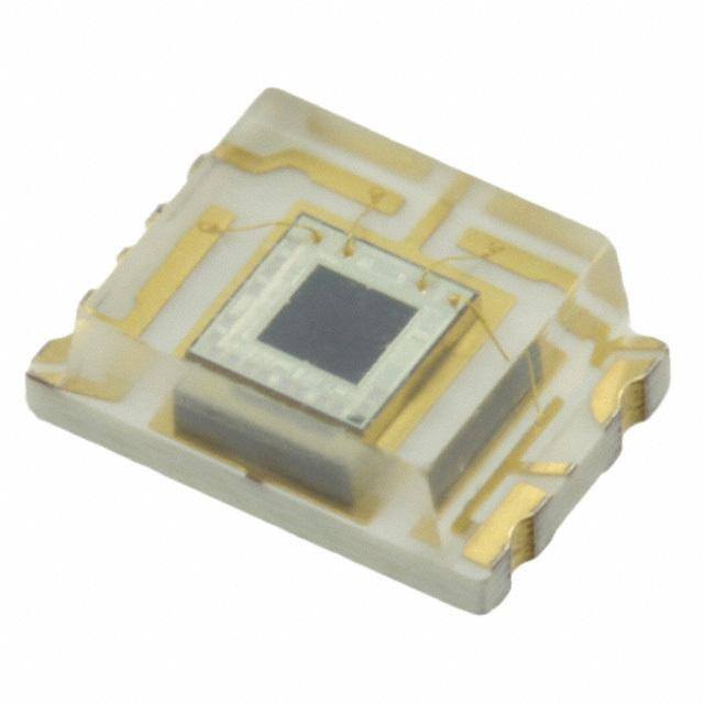
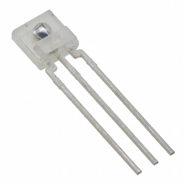
| 产品图片 |
|
| rohs | 符合RoHS无铅 / 符合限制有害物质指令(RoHS)规范要求 |
| 产品系列 | 光学传感器-光对频率和光对电压,ams TSL237T- |
| 数据手册 | http://www.ams.com/eng/content/download/250253/975957/143775 |
| 产品型号 | TSL237TTSL237T |
| 产品 | Light to Frequency Converters |
| 产品种类 | Light to Frequency Converters |
| 供应商器件封装 | 4-SMD |
| 其它名称 | TSL237-T |
| 包装 | 带卷 (TR) |
| 响应率 | 1.2 kHz/(uW/cm2) |
| 商标 | ams |
| 安装类型 | 表面贴装 |
| 安装风格 | SMD/SMT |
| 封装 | Reel |
| 封装/外壳 | 1510(3825 公制) |
| 封装/箱体 | SMD |
| 峰值波长 | 640 nm |
| 工作温度 | -40°C ~ 70°C |
| 工作电源电压 | 2.7 V to 5.5 V |
| 工厂包装数量 | 1000 |
| 带接近传感器 | 无 |
| 最大工作温度 | + 85 C |
| 最大频率 | 1 MHz |
| 最小工作温度 | - 40 C |
| 标准包装 | 1,000 |
| 波长 | 635nm |
| 电压-电源 | 2.7 V ~ 5.5 V |
| 电源电流 | 1.6 mA |
| 类型 | 环境 |
| 输出类型 | 频率 |


- 商务部:美国ITC正式对集成电路等产品启动337调查
- 曝三星4nm工艺存在良率问题 高通将骁龙8 Gen1或转产台积电
- 太阳诱电将投资9.5亿元在常州建新厂生产MLCC 预计2023年完工
- 英特尔发布欧洲新工厂建设计划 深化IDM 2.0 战略
- 台积电先进制程称霸业界 有大客户加持明年业绩稳了
- 达到5530亿美元!SIA预计今年全球半导体销售额将创下新高
- 英特尔拟将自动驾驶子公司Mobileye上市 估值或超500亿美元
- 三星加码芯片和SET,合并消费电子和移动部门,撤换高东真等 CEO
- 三星电子宣布重大人事变动 还合并消费电子和移动部门
- 海关总署:前11个月进口集成电路产品价值2.52万亿元 增长14.8%

PDF Datasheet 数据手册内容提取
TSL237T, TSL237CL High-Sensitivity Light-to-Frequency Converter General Description The TSL237 light-to-frequency converter combines a silicon photodiode and a current-to-frequency converter on a single monolithic CMOS integrated circuit. Output is a square wave (50% duty cycle) with frequency directly proportional to light intensity (irradiance) on the photodiode. The digital output allows direct interface to a microcontroller or other logic circuitry. Output enable (OE) places the output in a high-impedance state for multiple-unit sharing of a microcontroller input line. The device has been temperature compensated for the ultraviolet-to-visible light range of 320nm to 700nm and responds over the light range of 320nm to 1050nm. The TSL237 is characterized for operation over the temperature range of -40°C to 85°C and is supplied in a 4-lead ChipLED package (CL) and a compact 4-lead surface-mount package (T). OrderingInformation and ContentGuide appear at end of datasheet. Key Benefits & Features The benefits and features of the TSL237, High Sensitivity Light-to-Frequency Converter, are listed below: Figure 1: Added Value of Using TSL237 Benefits Features • High-Resolution Conversion of Light Intensity • 5M:1 Input Dynamic Range to Frequency with no External Components • Provides Low Light Level Operation • Low Dark Frequency of 0.1 Hz (typical), <2Hz at 50°C • Provides for High Sensitivity to Detect a Small • High Irradiance Responsivity 1.2kHz/(μW/cm2) Change in Light @ λp = 640nm • Reduces Board Space Requirements while • 2.6mm x 3.8mm 4-lead SMD (T) Package Simplifying Designs • 2.2mm x 2.5mm 4-lead ChipLED (CL) Package • Single-Supply Operation: 2.7V to 5.5V • Stable 200ppm/°C Temperature Coefficient • Communicates Directly with a Microcontroller ams Datasheet Page 1 [v1-00] 2016-Aug-22 DocumentFeedback
TSL237T, TSL237CL − General Description Block Diagram The functional blocks of this device are shown below: Figure 2: TSL237 Block Diagram Current-to-Frequency Light Photodiode Output Converter OE Page 2 ams Datasheet DocumentFeedback [v1-00] 2016-Aug-22
TSL237T, TSL237CL − Pin Assignments Pin Assignments Figure 3: Pin Diagram of Package T 4-Lead SMD (Top View) OE 1 4 OUT GND 2 3 V DD Figure 4: Pin Diagram of Package CL 4-Lead ChipLED (Top View) GND 1 4 OUT OE 2 3 V DD Figure 5: Terminal Functions Terminal Type Description T PKG CL PKG Name No. No. Power supply ground (substrate). All voltages are GND 2 1 referenced to GND. OE 1 2 I Enable for f (active low) O OUT 4 4 O Output frequency V 3 3 Supply voltage DD ams Datasheet Page 3 [v1-00] 2016-Aug-22 DocumentFeedback
TSL237T, TSL237CL − Absolute Maximum Ratings Absolute Maximum Ratings Stresses beyond those listed under Absolute Maximum Ratings may cause permanent damage to the device. These are stress ratings only. Functional operation of the device at these or any other conditions beyond those indicated under Recommended Operating Conditions is not implied. Exposure to absolute maximum rating conditions for extended periods may affect device reliability. Figure 6: Absolute Maximum Ratings Over Operating Free-Air Temperature Range (unless otherwise noted) Symbol Parameter Min Max Unit VDD Supply voltage (1) 6 V V Input voltage range, OE input -0.3 V + 0.3 V I DD TA Operating free-air temperature range (2) -40 85 °C TSTRG Storage temperature range (2) -40 85 °C Solder conditions in accordance with JEDEC J-STD-020A, 260 °C maximum temperature Note(s): 1. All voltage values are with respect to GND. 2. Long-term storage or operation above 70°C could cause package yellowing that will lower the sensitivity to wavelengths < 500nm. Page 4 ams Datasheet DocumentFeedback [v1-00] 2016-Aug-22
TSL237T, TSL237CL − Electrical Characteristics Electrical Characteristics All limits are guaranteed. The parameters with min and max values are guaranteed with production tests or SQC (Statistical Quality Control) methods. Figure 7: Recommended Operating Conditions Symbol Parameter Min Nom Max Unit V Supply voltage 2.7 5 5.5 V DD V High-level input voltage V = 5V 4.5 V V IH DD DD V Low-level input voltage V = 5V 0 0.5 V IL DD T Operating free-air temperature range -40 85 °C A Figure 8: Electrical Characteristics at V = 5V, T = 25°C (unless otherwise noted) DD A Symbol Parameter Test Conditions Min Typ Max Unit V High-level output voltage I = -1mA 4 4.7 V OH OH V Low-level output voltage I = 1mA 0.1 0.4 V OL OL I Supply current 1.6 3 mA DD Full-scale frequency (1) 500 1000 kHz Temperature coefficient of Wavelength ≤ 600nm, ±200 ppm/°C output frequency f = 50kHz O k Supply voltage sensitivity V = 5V ±10% ±0.5 %/V SVS DD Note(s): 1. Full-scale frequency is the maximum operating frequency of the device without saturation. ams Datasheet Page 5 [v1-00] 2016-Aug-22 DocumentFeedback
TSL237T, TSL237CL − Electrical Characteristics Figure 9: Operating Characteristics at V = 5V, T = 25°C, λ = 640nm (unless otherwise noted) DD A p Symbol Parameter Test Conditions Min Typ Max Unit fO Output frequency Ee = 40.4μW/cm2, 40 50 60 kHz E = 0μW/cm2 0 0.1 Hz e f Dark frequency D E = 0μW/cm2, e 0 2 Hz T = 50°C A kHz/ R Irradiance responsivity 1.2 e (μW/cm2) Nonlinearity (1) fO = 0kHz to 10kHz ±1% %F.S. Step response to full-scale 1 pulse of new frequency plus step input 1μs Time from OE low to 1 period of output frequency output enabled Note(s): 1. Nonlinearity is defined as the deviation of f from a straight line between zero and full scale, expressed as a percent of full scale. O Page 6 ams Datasheet DocumentFeedback [v1-00] 2016-Aug-22
TSL237T, TSL237CL − Typical Operating Characteristics Typical Operating Characteristics Figure 10: Output Frequency vs. Irradiance 1000 VDD = 5 V (cid:79)p = 640 nm Hz 100 TA = 25(cid:113)C k ) D 10 f(cid:239) O cy (f 1 n e u q e Fr 0.1 ut p ut O 0.01 0.001 0.001 0.01 0.1 1 10 100 1k Ee (cid:239) Irradiance (cid:239)(cid:3)(cid:80)W/cm2 Figure 11: Photodiode Spectral Responsivity 1 0.8 y vit si n o p 0.6 s e R d e z ali 0.4 m r o N 0.2 0 300 400 500 600 700 800 900 1000 1100 (cid:79) (cid:239) Wavelength (cid:239) nm ams Datasheet Page 7 [v1-00] 2016-Aug-22 DocumentFeedback
TSL237T, TSL237CL − Typical Operating Characteristics Figure 12: Supply Current vs. Free-Air Temperature 1.6 1.4 A m nt e 1.2 r r u C y pl p u 1 S D D I 0.8 0.6 (cid:239)40 (cid:239)15 10 35 60 85 TA (cid:239) Free-Air Temperature (cid:239) (cid:113)C Figure 13: Output Frequency vs. Free-Air Temperature 1.100 1.075 d e z ali 1.050 m r o N 1.025 y c n 1.000 e u q e Fr 0.975 ut p ut 0.950 O O 0.925 f 0.900 (cid:239)25 (cid:239)5 15 35 55 75 TA (cid:239) Free-Air Temperature (cid:239) (cid:113)C Page 8 ams Datasheet DocumentFeedback [v1-00] 2016-Aug-22
TSL237T, TSL237CL − Typical Operating Characteristics Figure 14: Dark Frequency vs. Free-Air Temperature 7.5 6.0 4.5 z H — 3.0 y c n 1.5 e u q e 0.0 r F k ar −1.5 D — −3.0 D f NOTE (cid:20) −4.5 −6.0 −7.5 −25 −5 15 35 55 75 TA − Free-Air Temperature − °C Note(s): 1. Internal offsets that result in dark frequency can be both positive and negative. The dashed line represents the case of negative offset in which an equivalent amount of light signal is required to obtain a non-zero output frequency. Figure 15: Photodiode Responsivity Temperature Coefficient vs. Wavelength of Incident Light 11k 10k C g 9k e d m/ 8k p p 7k nt 6k e ci effi 5k o C e 4k r u at 3k r e p m 2k e T 1k 0 600 650 700 750 800 850 900 950 1000 (cid:79) (cid:239) Wavelength of Incident Light (cid:239) nm ams Datasheet Page 9 [v1-00] 2016-Aug-22 DocumentFeedback
TSL237T, TSL237CL − Typical Operating Characteristics Figure 16: Normalized Output Voltage Vs. Angular Displacement - CL PKG 1 d e z 0.8 ali m or s N xi oltage — 0.6 Optical A V ut 0.4 p ut O — O 0.2 V Both Aspects (cid:3)(cid:2) (cid:4)(cid:2) 0 −90 −60 −30 0 30 60 90 (cid:2) − Angular Displacement − ° Figure 17: Normalized Output Voltage vs. Angular Displacement - T PKG NORMALIZED OUTPUT VOLTAGE vs. ANGULAR DISPLACEMENT — T PKG 1 d e z 0.8 ali m or s N xi oltage — 0.6 Optical A V ut 0.4 p ut O — O 0.2 V Side (cid:3)(cid:2) (cid:4)(cid:2) 0 −90 −60 −30 0 30 60 90 (cid:2) − Angular Displacement − ° Page 10 ams Datasheet DocumentFeedback [v1-00] 2016-Aug-22
TSL237T, TSL237CL − Typical Operating Characteristics Figure 18: Normalized Output Voltage vs. Angular Displacement - T PKG NORMALIZED OUTPUT VOLTAGE vs. ANGULAR DISPLACEMENT — T PKG 1 d e z 0.8 ali m or s N xi oltage — 0.6 Optical A V ut 0.4 p ut O — O 0.2 V End (cid:3)(cid:2) (cid:4)(cid:2) 0 −90 −60 −30 0 30 60 90 (cid:2) − Angular Displacement − ° ams Datasheet Page 11 [v1-00] 2016-Aug-22 DocumentFeedback
TSL237T, TSL237CL − Application Information Application Information Power-Supply Considerations Power-supply lines must be decoupled by a 0.01μF to 0.1μF capacitor with short leads placed close to the TSL237 (Figure19). A low-noise power supply is required to minimize jitter on output pulse. Figure 19: Typical TSL237 Interface to a Microcontroller VDD VDD 0.1 μF TSL237 Timer/Port OUT GND MCU OE Device Operational Details The frequency at the output pin (OUT) is given by: (EQ1) f = f + (R ) (E ) O D e e where • f is the output frequency O • f is the output frequency for dark condition (E = 0) D e • R is the device responsivity for a given wavelength of e light given in kHz/(μW/cm2) • E is the incident irradiance in μW/cm2 e f is a constant error term in the output frequency calculation D resulting from leakage currents, and is independent of light intensity. The TSL237 die is trimmed to minimize the magnitude of this dark frequency component so that it can be neglected in the transfer function calculation. Page 12 ams Datasheet DocumentFeedback [v1-00] 2016-Aug-22
TSL237T, TSL237CL − Application Information In many applications, measurement of the actual dark frequency may be impractical due to measurement times ranging from several seconds to several minutes, and the fact that some devices may never transition (zero dark frequency). Input Interface A low-impedance electrical connection between the device OE terminal and the device GND terminal is required for improved noise immunity. Output Interface The output of the device is designed to drive a CMOS logic input over short distances. If lines greater than 12 inches in length are used on the output, a buffer or line driver is recommended. Measuring the Frequency The choice of interface and measurement technique depends on the desired resolution and data acquisition rate. For maximum data-acquisition rate, period-measurement techniques are used. Period measurement requires the use of a fast reference clock with available resolution directly related to reference-clock rate. The technique is employed to measure rapidly varying light levels or to make a fast measurement of a constant light source. Maximum resolution and accuracy may be obtained using frequency-measurement, pulse-accumulation, or integration techniques. Frequency measurements provide the added benefit of averaging out random- or high-frequency variations (jitter) resulting from noise in the light signal. Resolution is limited mainly by available counter registers and allowable measurement time. Frequency measurement is well suited for slowly varying or constant light levels and for reading average light levels over short periods of time. Integration, the accumulation of pulses over a very long period of time, can be used to measure exposure - the amount of light present in an area over a given time period. Output enable (OE) places the output in a high-impedance state for multiple-unit sharing of a microcontroller input line. When the OE line goes low, the device resynchronizes the output to an integration cycle. The rising edge of the output signal (OUT) will occur exactly one period of the output frequency after OE goes low. ams Datasheet Page 13 [v1-00] 2016-Aug-22 DocumentFeedback
TSL237T, TSL237CL − Application Information PCB Pad Layout Suggested PCB pad layout guidelines for the T package are shown in Figure20. Figure 20: Suggested T Package PCB Layout 0.90 1.00 1.50 2.90 Note(s): 1. All linear dimensions are in millimeters. 2. This drawing is subject to change without notice. Page 14 ams Datasheet DocumentFeedback [v1-00] 2016-Aug-22
TSL237T, TSL237CL − Application Information Suggested PCB pad layout guidelines for the CL package are shown in Figure21. Figure 21: Suggested CL Package PCB Layout 0.95 0.55 0.75 1.60 2.10 Note(s): 1. All linear dimensions are in millimeters. 2. This drawing is subject to change without notice. ams Datasheet Page 15 [v1-00] 2016-Aug-22 DocumentFeedback
TSL237T, TSL237CL − Packaging Mechanical Data Packaging Mechanical Data The TSL237 is supplied in a low-profile surface-mount package. This package contains no lead (Pb). Figure 22: Package T - Four-Lead Surface Mount Device Packaging Configuration TOP VIEW 1.89 2.60 1.0 3.80 Photo-Active DETAIL A: TYPICAL PACKAGE TERMINAL Area (Note C) SIDE VIEW 0.10 0.90 3.10 7(cid:2) 0.35 0.40 ÎÎÎ 0.80 1.3È5 ÈÈÈÎÈÎÈÎÈÈ 0.45 ÈÈÈÈÈÈÈÈ R 0.20 0.50 BOTTOM VIEW A 1.50 RoHS P PIN 1 Lead 0.55 Green Note(s): 1. All linear dimensions are in millimeters. 2. Terminal finish is gold, 1.3μm minimum. 3. The center of the 0.84mm × 0.84mm integrated photodiode active area is referenced to the upper left corner of the package (near Pin 1). 4. Dimension tolerance is ±0.15mm. 5. This drawing is subject to change without notice. Page 16 ams Datasheet DocumentFeedback [v1-00] 2016-Aug-22
TSL237T, TSL237CL − Packaging Mechanical Data The TSL237CL is supplied in a low-profile surface-mount package. This package contains no lead (Pb). Figure 23: Package CL - Four-Lead ChipLED Plastic Surface Mount Packaging Configuration TOP VIEW PIN OUT Pin 1 Marker TOP VIEW 1.084 Pin 1 Marker 1.1 1 4 2.2 (cid:3) 0.1 2 3 2.5 (cid:3) 0.1 Photo-Active Area (Note B) SIDE VIEW 0.65 (cid:3) 0.1 0.47 0.18 BOTTOM VIEW 2.1 0.05 0.5 1.6 RoHS Green Pin 1 0.2 0.3 0.2 Note(s): 1. All linear dimensions are in millimeters. Dimension tolerance is ± 0.05 mm unless otherwise noted. 2. The center of the 0.84mm × 0.84mm integrated photodiode active area is referenced to the upper left corner of the package (near Pin 1). 3. Package top surface is molded with an electrically nonconductive clear plastic compound having an index of refraction of 1.55. 4. Contact finish is soft gold plated. 5. This drawing is subject to change without notice. ams Datasheet Page 17 [v1-00] 2016-Aug-22 DocumentFeedback
TSL237T, TSL237CL − Packaging Mechanical Data Figure 24: Package T - Four Lead Surface Mount Package Carrier Tape 0.30 (cid:2) 0.050 2.10 SIDE VIEW 1.75 (cid:2) 0.100 B (cid:4) 1.50 4 (cid:2) 0.100 END VIEW 8 Typ 2 (cid:2) 0.100 TOP VIEW 12 (cid:2) 0.100 5.50 (cid:2) 0.100 (cid:4) 1.50 R 0.20 TYP B A A DETAIL B DETAIL A 2.90 (cid:2) 0.100 Ao 3.09 MAX R 0.20 TYP R 0.20 TYP 4.29 MAX 4.10 (cid:2) 0.100 Bo 1.80 Ko Note(s): 1. All linear dimensions are in millimeters. 2. The dimensions on this drawing are for illustrative purposes only. Dimensions of an actual carrier may vary slightly. 3. Symbols on drawing Ao, Bo, and Ko are defined in ANSI EIA Standard 481−B 2001. 4. Each reel is 178 millimeters in diameter and contains 1000 parts. 5. ams packaging tape and reel conform to the requirements of EIA Standard 481−B. 6. In accordance with EIA standard, device pin 1 is located next to the sprocket holes in the tape. 7. This drawing is subject to change without notice. Page 18 ams Datasheet DocumentFeedback [v1-00] 2016-Aug-22
TSL237T, TSL237CL − Packaging Mechanical Data Figure 25: Package CL - Four Lead ChipLED Plastic Surface Mount Packaging Configuration TOP VIEW 2.00 (cid:3) 0.05 1.75 (cid:3) 1.50 4.00 4.00 + 0.10 B + 0.30 8.0 − 0.10 3.50 (cid:3) 0.05 (cid:3) 1.00 (cid:3) 0.25 A A B DETAIL A DETAIL B 5(cid:2) Max 5(cid:2) Max 0.25 2.35 (cid:3) 0.05 (cid:3) 0.02 2.75 (cid:3) 0.05 0.80 (cid:3) 0.05 Ao Bo Ko Note(s): 1. All linear dimensions are in millimeters. Dimension tolerance is ± 0.10 mm unless otherwise noted. 2. The dimensions on this drawing are for illustrative purposes only. Dimensions of an actual carrier may vary slightly. 3. Symbols on drawing Ao, Bo, and Ko are defined in ANSI EIA Standard 481−B 2001. 4. Each reel is 178 millimeters in diameter and contains 1000 parts. 5. ams packaging tape and reel conform to the requirements of EIA Standard 481−B. 6. In accordance with EIA standard, device pin 1 is located next to the sprocket holes in the tape. 7. This drawing is subject to change without notice. ams Datasheet Page 19 [v1-00] 2016-Aug-22 DocumentFeedback
TSL237T, TSL237CL − Manufacturing Information Manufacturing Information The reflow profile specified here describes expected maximum heat exposure of devices during the solder reflow process of the device on a PWB. Temperature is measured at the top of the device. Devices should be limited to one pass through the solder reflow profile. Figure 26: TSL237 Solder Reflow Profile Parameter Reference TSL237T TSL237CL Average temperature gradient in preheating 2.5°C/s 2.5°C/s Soak time t 2 to 3 minutes 2 to 3 minutes soak Time above T , 217°C t Max 60 s Max 60 s 1 1 Time above T , 230°C t Max 50 s Max 50 s 2 2 Time above T , (T - 10°C) t Max 10 s Max 10 s 3 peak 3 Peak temperature in reflow T 260°C (-0°C/5°C) 260°C (-0°C/5°C) peak Temperature gradient in cooling Max -5°C/s Max -5°C/s Figure 27: Solder Reflow Profile Not to scale — for reference only T peak T 3 T 2 T 1 C) (cid:2) e ( r u at r e p m e T Time (s) t 3 t 2 tsoak t1 Page 20 ams Datasheet DocumentFeedback [v1-00] 2016-Aug-22
TSL237T, TSL237CL − Manufacturing Information Moisture Sensitivity Optical characteristics of the device can be adversely affected during the soldering process by the release and vaporization of moisture that has been previously absorbed into the package molding compound. To ensure the package molding compound contains the smallest amount of absorbed moisture possible, each device is dry−baked prior to being packed for shipping. Devices are packed in a sealed aluminized envelope with silica gel to protect them from ambient moisture during shipping, handling, and storage before use. The CL and T packages have been assigned a moisture sensitivity level of MSL 3 and the devices should be stored under the following conditions: • Temperature Range: 5°C to 50°C • Relative Humidity: 60% maximum • Total Time: 12 months from the date code on the aluminized envelope - if unopened • Opened Time: 168 hours or fewer Rebaking will be required if the devices have been stored unopened for more than 12 months or if the aluminized envelope has been open for more than 168 hours. If rebaking is required, it should be done at 50°C for 12 hours. ams Datasheet Page 21 [v1-00] 2016-Aug-22 DocumentFeedback
TSL237T, TSL237CL − Ordering & Contact Information Ordering & Contact Information Figure 28: Ordering Information Ordering Package Device T Package - Leads A Code Designator TSL237T TSL237 -40°C to 85°C 4-lead Low Profile Surface Mount T TSL237CL TSL237 -40°C to 85°C 4-lead ChipLED CL Buy our products or get free samples online at: www.ams.com/ICdirect Technical Support is available at: www.ams.com/Technical-Support Provide feedback about this document at: www.ams.com/Document-Feedback For further information and requests, e-mail us at: ams_sales@ams.com For sales offices, distributors and representatives, please visit: www.ams.com/contact Headquarters ams AG Tobelbader Strasse 30 8141 Premstaetten Austria, Europe Tel: +43 (0) 3136 500 0 Website: www.ams.com Page 22 ams Datasheet DocumentFeedback [v1-00] 2016-Aug-22
TSL237T, TSL237CL − RoHS Compliant & ams Green Statement RoHS Compliant & ams Green RoHS: The term RoHS compliant means that ams AG products fully comply with current RoHS directives. Our semiconductor Statement products do not contain any chemicals for all 6 substance categories, including the requirement that lead not exceed 0.1% by weight in homogeneous materials. Where designed to be soldered at high temperatures, RoHS compliant products are suitable for use in specified lead-free processes. ams Green (RoHS compliant and no Sb/Br): ams Green defines that in addition to RoHS compliance, our products are free of Bromine (Br) and Antimony (Sb) based flame retardants (Br or Sb do not exceed 0.1% by weight in homogeneous material). Important Information: The information provided in this statement represents ams AG knowledge and belief as of the date that it is provided. ams AG bases its knowledge and belief on information provided by third parties, and makes no representation or warranty as to the accuracy of such information. Efforts are underway to better integrate information from third parties. ams AG has taken and continues to take reasonable steps to provide representative and accurate information but may not have conducted destructive testing or chemical analysis on incoming materials and chemicals. ams AG and ams AG suppliers consider certain information to be proprietary, and thus CAS numbers and other limited information may not be available for release. ams Datasheet Page 23 [v1-00] 2016-Aug-22 DocumentFeedback
TSL237T, TSL237CL − Copyrights & Disclaimer Copyrights & Disclaimer Copyright ams AG, Tobelbader Strasse 30, 8141 Premstaetten, Austria-Europe. Trademarks Registered. All rights reserved. The material herein may not be reproduced, adapted, merged, translated, stored, or used without the prior written consent of the copyright owner. Devices sold by ams AG are covered by the warranty and patent indemnification provisions appearing in its General Terms of Trade. ams AG makes no warranty, express, statutory, implied, or by description regarding the information set forth herein. ams AG reserves the right to change specifications and prices at any time and without notice. Therefore, prior to designing this product into a system, it is necessary to check with ams AG for current information. This product is intended for use in commercial applications. Applications requiring extended temperature range, unusual environmental requirements, or high reliability applications, such as military, medical life-support or life-sustaining equipment are specifically not recommended without additional processing by ams AG for each application. This product is provided by ams AG “AS IS” and any express or implied warranties, including, but not limited to the implied warranties of merchantability and fitness for a particular purpose are disclaimed. ams AG shall not be liable to recipient or any third party for any damages, including but not limited to personal injury, property damage, loss of profits, loss of use, interruption of business or indirect, special, incidental or consequential damages, of any kind, in connection with or arising out of the furnishing, performance or use of the technical data herein. No obligation or liability to recipient or any third party shall arise or flow out of ams AG rendering of technical or other services. Page 24 ams Datasheet DocumentFeedback [v1-00] 2016-Aug-22
TSL237T, TSL237CL − Document Status Document Status Document Status Product Status Definition Information in this datasheet is based on product ideas in the planning phase of development. All specifications are Product Preview Pre-Development design goals without any warranty and are subject to change without notice Information in this datasheet is based on products in the design, validation or qualification phase of development. Preliminary Datasheet Pre-Production The performance and parameters shown in this document are preliminary without any warranty and are subject to change without notice Information in this datasheet is based on products in ramp-up to full production or full production which Datasheet Production conform to specifications in accordance with the terms of ams AG standard warranty as given in the General Terms of Trade Information in this datasheet is based on products which conform to specifications in accordance with the terms of Datasheet (discontinued) Discontinued ams AG standard warranty as given in the General Terms of Trade, but these products have been superseded and should not be used for new designs ams Datasheet Page 25 [v1-00] 2016-Aug-22 DocumentFeedback
TSL237T, TSL237CL − Revision Information Revision Information Changes from 055K (2010-Aug) to current revision 1-00 (2016-Aug-22) Page Content of TAOS datasheet was converted to the latest ams design Added Figure 1 1 Updated Figure 5 3 Note(s): 1. Page and figure numbers for the previous version may differ from page and figure numbers in the current revision. 2. Correction of typographical errors is not explicitly mentioned. Page 26 ams Datasheet DocumentFeedback [v1-00] 2016-Aug-22
TSL237T, TSL237CL − Content Guide Content Guide 1 General Description 1 Key Benefits & Features 2 Block Diagram 3 Pin Assignments 4 Absolute Maximum Ratings 5 Electrical Characteristics 7 Typical Operating Characteristics 12 Application Information 12 Power-Supply Considerations 12 Device Operational Details 13 Input Interface 13 Output Interface 13 Measuring the Frequency 14 PCB Pad Layout 16 Packaging Mechanical Data 20 Manufacturing Information 21 Moisture Sensitivity 22 Ordering & Contact Information 23 RoHS Compliant & ams Green Statement 24 Copyrights & Disclaimer 25 Document Status 26 Revision Information ams Datasheet Page 27 [v1-00] 2016-Aug-22 DocumentFeedback
Mouser Electronics Authorized Distributor Click to View Pricing, Inventory, Delivery & Lifecycle Information: a ms: TSL237T