ICGOO在线商城 > 传感器,变送器 > 光学传感器 - 环境光,IR,UV 传感器 > ISL29011IROZ-T7
 Datasheet下载
- 型号: ISL29011IROZ-T7
- 制造商: Intersil
- 库位|库存: xxxx|xxxx
- 要求:
| 数量阶梯 | 香港交货 | 国内含税 |
| +xxxx | $xxxx | ¥xxxx |
查看当月历史价格
查看今年历史价格
ISL29011IROZ-T7产品简介:
ICGOO电子元器件商城为您提供ISL29011IROZ-T7由Intersil设计生产,在icgoo商城现货销售,并且可以通过原厂、代理商等渠道进行代购。 ISL29011IROZ-T7价格参考¥22.26-¥48.84。IntersilISL29011IROZ-T7封装/规格:光学传感器 - 环境光,IR,UV 传感器, Optical Sensor Ambient 550nm I²C 8-VFDFN Exposed Pad。您可以下载ISL29011IROZ-T7参考资料、Datasheet数据手册功能说明书,资料中有ISL29011IROZ-T7 详细功能的应用电路图电压和使用方法及教程。
Renesas Electronics America Inc.的型号为ISL29011IROZ-T7的传感器,属于光学传感器中的环境光、红外(IR)和紫外(UV)传感器类别。该传感器的主要应用场景包括:

1. 消费类电子产品:如智能手机、平板电脑等便携设备中,用于自动调节屏幕亮度,从而提升用户体验并节省电池电量。

2. 工业控制系统:在需要根据环境光照变化进行自动控制的场合,如自动照明系统、安防摄像头的光线补偿控制等。

3. 智能家居与家电:应用于智能灯具、窗帘控制器等设备中,实现基于环境光强度的自动化控制。

4. 汽车电子:可用于车载显示系统或车内照明系统的环境光感应模块,提升驾驶舒适性与安全性。

5. 可穿戴设备:如智能手表、健康监测设备等,帮助设备适应不同光照条件下的显示需求。

该传感器具备高灵敏度和宽动态范围,适合多种光照环境下的精确测量,支持红外线检测功能,适用于需要区分可见光与红外光的应用场景。
| 参数 | 数值 |
| 产品目录 | |
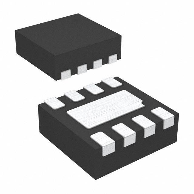
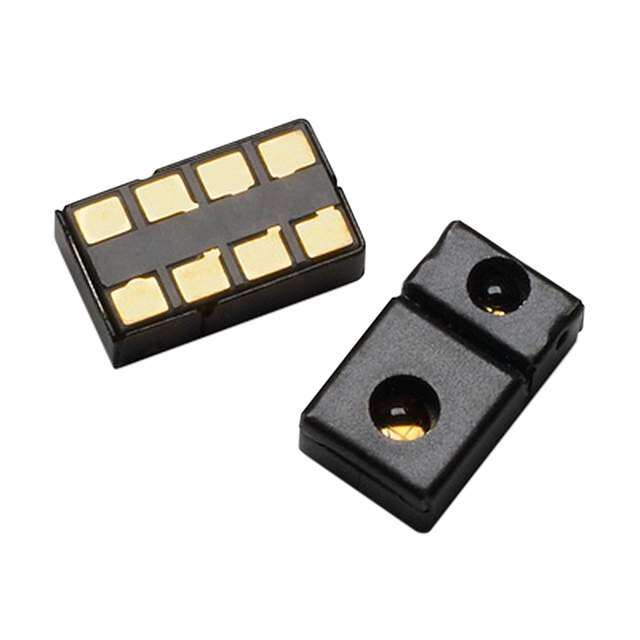
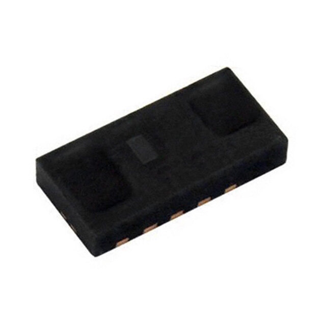
| 描述 | IC PROXIMITY SENSOR AMB LT 8ODFN |
| 产品分类 | |
| 品牌 | Intersil |
| 数据手册 | |
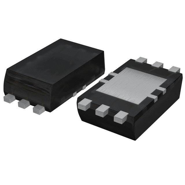
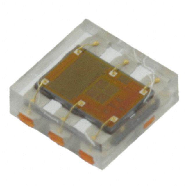
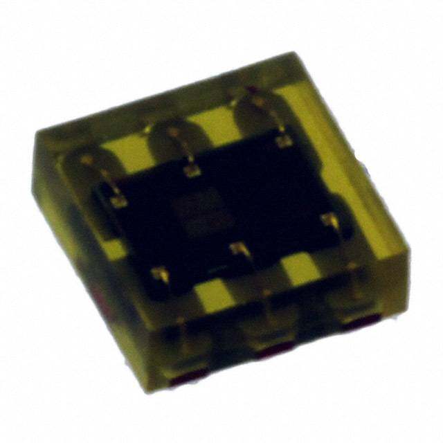
| 产品图片 |
|
| 产品型号 | ISL29011IROZ-T7 |
| rohs | 无铅 / 符合限制有害物质指令(RoHS)规范要求 |
| 产品系列 | - |
| 供应商器件封装 | 8-ODFN(2.1x2) |
| 其它名称 | ISL29011IROZ-T7DKR |
| 包装 | Digi-Reel® |
| 安装类型 | 表面贴装 |
| 封装/外壳 | 8-VFDFN 裸露焊盘 |
| 工作温度 | -40°C ~ 85°C |
| 带接近传感器 | 是 |
| 标准包装 | 1 |
| 波长 | 550nm |
| 电压-电源 | 2.25 V ~ 3.63 V |
| 类型 | 环境 |
| 输出类型 | I²C |


- 商务部:美国ITC正式对集成电路等产品启动337调查
- 曝三星4nm工艺存在良率问题 高通将骁龙8 Gen1或转产台积电
- 太阳诱电将投资9.5亿元在常州建新厂生产MLCC 预计2023年完工
- 英特尔发布欧洲新工厂建设计划 深化IDM 2.0 战略
- 台积电先进制程称霸业界 有大客户加持明年业绩稳了
- 达到5530亿美元!SIA预计今年全球半导体销售额将创下新高
- 英特尔拟将自动驾驶子公司Mobileye上市 估值或超500亿美元
- 三星加码芯片和SET,合并消费电子和移动部门,撤换高东真等 CEO
- 三星电子宣布重大人事变动 还合并消费电子和移动部门
- 海关总署:前11个月进口集成电路产品价值2.52万亿元 增长14.8%

PDF Datasheet 数据手册内容提取
DATASHEET ISL29011 FN6467 Digital Ambient Light Sensor and Proximity Sensor with Interrupt Function Rev 6.00 May 1, 2014 The ISL29011 is an integrated ambient and infrared Features light-to-digital converter with a built-in IR LED driver and I2C Interface (SMBus Compatible). This device provides not only Proximity Sensing ambient light sensing to allow robust backlight/display brightness • Ambient IR cancellation during proximity sensing control but also infrared sensing to allow proximity estimation - Works under direct sunlight featured with interrupt function. • IR LED driver with programmable source current For ambient light sensing, an internal ADC has been designed - Adjustable current drive from 100mA to 12.5mA based on the charge-balancing A/D conversion technique. The ADC conversion time is nominally 90ms and is user adjustable • Programmable LED current modulation frequency from 11µs to 90ms, depending on oscillator frequency and ADC • Variable conversion resolution resolution. This ADC is capable of rejecting 50Hz and 60Hz flicker noise caused by artificial light sources. The lux-range-select Ambient Light Sensing feature allows users to program the lux range for optimized • Simple output code directly proportional to lux counts/lux. • Adjustable sensitivity up to 65 counts per lux For proximity sensing, the ADC is used to digitize the output signal • Selectable range (via I2C) from the photodiode array when the internal IR LED driver is - Range 1 = 0.015 lux to 1,000 lux turned on and off for the programmed time periods under user-selected modulation frequency to drive the external IR LED. - Range 2 = 0.06 lux to 4,000 lux As this proximity sensor employs a noise cancellation scheme to - Range 3 = 0.24 lux to 16,000 lux highly reject unwanted IR noise, the digital output of proximity - Range 4 = 0.96 lux to 64,000 lux sensing decreases with distance. The driver output current is user selectable up to 100mA to drive different types of IR emitter • Integrated 50Hz/60Hz noise rejection LEDs. • Works under various light sources, including sunlight Six different modes of operation can be selected via the I2C Ideal Spectral Response for Light and Proximity Sensor interface: Programmable ALS once with auto power-down, • Light sensor close to human eye response programmable IR sensing once, programmable proximity sensing once, programmable continuous ALS sensing, programmable - Excellent light sensor IR and UV rejection continuous IR sensing and programmable continuous proximity • Proximity sensor range from 850nm to 950nm sensing. The programmable one-time operation modes greatly - Can use either 850nm or 950nm LED solution reduce power because an immediate automatic shutdown reduces overall supply current less than 0.5µA. Ultra Low Power The ISL29011 supports both hardware and software interrupts • 90µA max operating current that remain asserted until the host clears it through the I2C • Software shutdown and automatic shutdown interface for ambient light sensing and proximity detection. - 0.5µA max shutdown current Designed to operate on supplies from 2.25V to 3.63V, the Easy to Use ISL29011 is specified for operation over the -40°C to +85°C ambient temperature range. It is packaged in a clear, Pb-free 8 Ld • I2C (SMBus compatible) output ODFN package. • No complex algorithms needed Applications • Temperature compensated • Small form factor • Display and keypad dimming adjustment and proximity - 8 Ld 2.0mmx2.1mmx0.7mm ODFN package sensing for: - Mobile devices: smart phone, PDA, GPS Additional Features - Computing devices: Notebook PC, Webpad • I2C and SMBus compatible - Consumer devices: LCD-TV, digital picture frame, digital • 1.7V to 3.63V supply for I2C interface camera • 2.25V to 3.63V sensor power supply • Industrial and medical light and proximity sensing • Pb-Free (RoHS compliant) FN6467 Rev 6.00 Page 1 of 19 May 1, 2014
ISL29011 Ordering Information PACKAGE PART NUMBER TEMP. RANGE Tape and Reel PKG. (Notes 1, 2, 3) (°C) (Pb-Free) DWG. # ISL29011IROZ-T7 -40 to +85 8 Ld ODFN L8.2.1x2.0 ISL29011IROZ-EVALZ Evaluation Board NOTES: 1. Please refer to TB347 for details on reel specifications. 2. These Intersil Pb-free plastic packaged products employ special Pb-free material sets; molding compounds/die attach materials and NiPdAu plate-e4 termination finish, which is RoHS compliant and compatible with both SnPb and Pb-free soldering operations. Intersil Pb-free products are MSL classified at Pb-free peak reflow temperatures that meet or exceed the Pb-free requirements of IPC/JEDEC J STD-020. 3. For Moisture Sensitivity Level (MSL), please see device information page for ISL29011. For more information on MSL, please see tech brief TB477. Pin Configuration ISL29011 (8 LD ODFN) TOP VIEW) VDDD 1 8 IRDR VDDA 2 7 INT GND 3 6 SDA REXT 4 5 SCL EXPOSED PAD CAN BE CONNECTED TO GND OR ELECTRICALLY ISOLATED Pin Descriptions PIN NUMBER PIN NAME DESCRIPTION 1 VDDD Positive digital supply: 2.25V to 3.63V. 2 VDDA Positive analog supply: 2.25V to 3.63V, VDDA and VDDD should be externally shorted. 3 GND Ground. The thermal pad is also connected to the GND pin. 4 REXT External resistor pin setting the internal reference current and the conversion time. 499kΩ with a 1% tolerance resistor is recommended. 5 SCL I2C serial clock line The I2C bus lines can be pulled from 1.7V to above VDD, 3.63V max. 6 SDA I2C serial data line 7 INT Interrupt pin; LO for interrupt/alarming. The INT pin is an open drain. 8 IRDR IR LED driver pin connecting to the anode of the external IR LED. The source current of the IR LED driver can be programmed through I2C. Exposed pad connected to ground or electrically isolated. FN6467 Rev 6.00 Page 2 of 19 May 1, 2014
ISL29011 Block Diagram VDDA VDDD 2 1 PHOTODIODE ARRAY COMMAND REGISTER LIGHT DATA INTEGRATION PROCESS DATA ADC ALS AND IR REGISTER 6 SDA IR PHOTODIODE I2C 5 SCL ARRAY IREF INTERRUPT 7 INT FOSC ISL29011 IR DRIVER 8 IRDR 4 3 REXT GND FN6467 Rev 6.00 Page 3 of 19 May 1, 2014
ISL29011 Absolute Maximum Ratings (TA = +25°C) Thermal Information VSUP(VDDD,VDDA) Supply Voltage between VDD and GND. . . . . . . . . . . . 4V Thermal Resistance (Typical) . . . . . . . . . . . . . JA (°C/W) JC (°C/W) VDDA Supply Voltage between VDDA and GND . . . . . . . . . . . . .VDDD ± 0.5V 8 Ld ODFN (Notes 4, 5) . . . . . . . . . . . . . . . . 88 14 I2C Bus (SCL, SDA) and INT Pin Voltage . . . . . . . . . . . . . . . . . . . -0.2V to 4V Maximum Die Temperature . . . . . . . . . . . . . . . . . . . . . . . . . . . . . . . . .+90°C I2C Bus (SCL, SDA) and INT Pin Current . . . . . . . . . . . . . . . . . . . . . . <10mA Storage Temperature. . . . . . . . . . . . . . . . . . . . . . . . . . . . . .-40°C to +100°C IRDR Pin Voltage . . . . . . . . . . . . . . . . . . . . . . . . . . . . . . .-0.2V to VDD + 0.5V Operating Temperature . . . . . . . . . . . . . . . . . . . . . . . . . . . . .-40°C to +85°C REXT Pin Voltage. . . . . . . . . . . . . . . . . . . . . . . . . . . . . . . .-0.2V to VDD + 0.5V Pb-Free Reflow Profile (*) . . . . . . . . . . . . . . . . . . . . . . . . . . . . . . . see TB477 ESD Rating *Peak temperature during solder reflow +235°C max Human Body Model . . . . . . . . . . . . . . . . . . . . . . . . . . . . . . . . . . . . . . . . 3kV CAUTION: Do not operate at or near the maximum ratings listed for extended periods of time. Exposure to such conditions may adversely impact product reliability and result in failures not covered by warranty. NOTE: 4. JA is measured in free air with the component mounted on a high effective thermal conductivity test board with “direct attach” features. See Tech Brief TB379. 5. For JC, the “case temp” location is the center of the exposed metal pad on the package underside. IMPORTANT NOTE: All parameters having Min/Max specifications are guaranteed. Typical values are for information purposes only. Unless otherwise noted, all tests are at the specified temperature and are pulsed tests, therefore: TJ = TC = TA Electrical Specifications VSUP(VDDD,VDDA) = 3V, TA = +25°C, REXT = 499kΩ 1% tolerance, 16-bit ADC operation, unless otherwise specified. MIN MAX PARAMETER DESCRIPTION TEST CONDITIONS (Note 10) TYP (Note 10) UNITS VSUP Power Supply Range for VDDD, VDDA (Note 6) 2.25 3.63 V SR_VDD Required Input Power-up Slew Rate VDD rising edge between 0.4V and 2.25V 0.5 V/ms ISUP(OFF) Supply Current when Powered Down Software disabled or auto power-down 0.1 0.5 µA ISUP(ON) Supply Current of Ambient Light and 70 90 µA IR Sensing fOSC Internal Oscillator Frequency 675 750 825 kHz tint ADC Integration/Conversion Time 16-bit ADC data 90 ms FI2C I2C Clock Rate Range 1 to 400 kHz DATA_0 Count Output When Dark E = 0 lux 1 5 Counts DATA_FS Full Scale ADC Code 65535 Counts DATA Count Output Variation Over Three Ambient light sensing ±10 % DATA Light Sources: Fluorescent, Incandescent and Sunlight DATA_1 Light Count Output With LSB of E = 300 lux, Fluorescent light (Note 7), Ambient 15000 20000 25000 Counts 0.015lux/count light sensing, Range 1 (1k lux) DATA_2 Light Count Output With LSB of E = 300 lux, Fluorescent light (Note 7), Ambient 5000 Counts 0.06lux/count light sensing, Range 2 (4k lux) DATA_3 Light Count Output With LSB of E = 300 lux, Fluorescent light (Note 7), Ambient 1250 Counts 0.24lux/count light sensing, Range 3 (16k lux) DATA_4 Light Count Output With LSB of E = 300 lux, Fluorescent light (Note 7), Ambient 312 Counts 0.96lux/count light sensing, Range 4 (64k lux) DATA_IR1 Infrared Count Output E = 210 lux, Sunlight (Note 8), IR sensing, Range 1 15000 20000 25000 Counts DATA_IR2 Infrared Count Output E = 210 lux, Sunlight (Note 8), IR sensing, Range 2 5000 Counts DATA_IR3 Infrared Count Output E = 210 lux, Sunlight (Note 8), IR sensing, Range 3 1250 Counts DATA_IR4 Infrared Count Output E = 210 lux, Sunlight (Note 8), IR sensing, Range 4 312 Counts VREF Voltage of REXT Pin 0.52 V FN6467 Rev 6.00 Page 4 of 19 May 1, 2014
ISL29011 Electrical Specifications VSUP(VDDD,VDDA) = 3V, TA = +25°C, REXT = 499kΩ 1% tolerance, 16-bit ADC operation, unless otherwise specified. (Continued) MIN MAX PARAMETER DESCRIPTION TEST CONDITIONS (Note 10) TYP (Note 10) UNITS IINT INT Current Sinking Capability 4 5 mA IIRDR1 IRDR Source Current IS<1:0> = 0 15Ω at IRDR pin 100 mA (Note 9) IIRDR2 IRDR Source Current IS<1:0> = 1 44 50 58 mA (Note 9) IIRDR3 IRDR Source Current IS<1:0> = 2 25 mA (Note 9) IIRDR4 IRDR Source Current IS<1:0> = 3 12.5 mA (Note 9) VIRLED Voltage Head Room of IRDR Pin IRDR = 90mA, IS<1:0> = 0 (Note 9) VDD - 1.0 V tr Rise Time for IRDR Source Current RLOAD = 15Ω at IRDR pin, 20% to 80% 35 ns tf Fall Time for IRDR Source Current RLOAD = 15Ω at IRDR pin, 80% to 20% 10 ns fIRLED1 IR LED Modulation Frequency Frequency = 0 (Note 9) DC kHz fIRLED2 IR LED Modulation Frequency Frequency = 1 (Note 9) 360 kHz ISUP (IRLED1) Supply Current of Proximity Sensing IS<1:0> = 0, Frequency = 0 (Note 9) 101 mA ISUP (IRLED2) Supply Current of Proximity Sensing IS<1:0> = 0, Frequency = 1 (Note 9) 51 mA Duty Cycle Duty Cycle of IR LED Modulation 50 % PROX-IR Differential ADC Output of IR and IR and proximity sensing with Range 2 and 1.0 % PROX Proximity Sensing With Object Far Scheme0; 15Ω @ IRDR pin, IS<1:0> = 0, Away to Provide No Reflection Frequency = 0; E = 210 lux, Sunlight. NOTES: 6. VSUP is the common voltage to VDDD and VDDA. 7. 550nm green LED is used in production test. The 550nm LED irradiance is calibrated to produce the same DATA count against an illuminance level of 300 lux fluorescent light. 8. 850nm infrared LED is used in production test. The 850nm LED irradiance is calibrated to produce the same DATA_IR count against an illuminance level of 210 lux sunlight at sea level. 9. See “Register Set” on page10. 2 I C Electrical Specifications For SCL and SDA unless otherwise noted, VSUP(VDDD,VDDA) = 3V, TA = +25°C, REXT = 499kΩ 1% tolerance, 16-bit ADC operation. MIN MAX PARAMETER DESCRIPTION TEST CONDITIONS (Note 10) TYP (Note 10) UNITS VI2C Supply Voltage Range for I2C Interface 1.7 3.63 V fSCL SCL Clock Frequency 400 kHz VIL SCL and SDA Input Low Voltage 0.55 V VIH SCL and SDA Input High Voltage 1.25 V Vhys Hysteresis of Schmitt Trigger Input 0.05VDD V VOL Low-Level Output Voltage (Open-drain) at 0.4 V 4mA Sink Current Ii Input Leakage for Each SDA, SCL Pin -10 10 µA tSP Pulse Width of Spikes that must be 50 ns Suppressed by the Input Filter tAA SCL Falling Edge to SDA Output Data Valid 900 ns FN6467 Rev 6.00 Page 5 of 19 May 1, 2014
ISL29011 2 I C Electrical Specifications For SCL and SDA unless otherwise noted, VSUP(VDDD,VDDA) = 3V, TA = +25°C, REXT = 499kΩ 1% tolerance, 16-bit ADC operation. (Continued) MIN MAX PARAMETER DESCRIPTION TEST CONDITIONS (Note 10) TYP (Note 10) UNITS Ci Capacitance for each SDA and SCL pin 10 pF tHD:STA Hold Time (Repeated) START Condition After this period, the first clock pulse 600 ns is generated. tLOW LOW Period of the SCL clock Measured at the 30% of VDD crossing 1300 ns tHIGH HIGH period of the SCL Clock 600 ns tSU:STA Set-up Time for a Repeated START Condition 600 ns tHD:DAT Data Hold Time 30 ns tSU:DAT Data Set-up Time 100 ns tR Rise Time of both SDA and SCL Signals 20 + 0.1xCb ns tF Fall Time of both SDA and SCL Signals 20 + 0.1xCb ns tSU:STO Set-up Time for STOP Condition 600 ns tBUF Bus Free Time Between a STOP and START 1300 ns Condition Cb Capacitive Load for Each Bus Line 400 pF Rpull-up SDA and SCL System Bus Pull-Up Resistor Maximum is determined by tR and tF 1 kΩ tVD;DAT Data Valid Time 0.9 µs tVD:ACK Data Valid Acknowledge Time 0.9 µs VnL Noise Margin at the LOW Level 0.1VDD V VnH Noise Margin at the HIGH Level 0.2VDD V NOTE: 10. Compliance to datasheet limits is assured by one or more methods: production test, characterization and/or design. FN6467 Rev 6.00 Page 6 of 19 May 1, 2014
ISL29011 FIGURE 1. I2C TIMING DIAGRAM Principles of Operation power-down mode automatically after one conversion is finished and keep the conversion data available for the master to fetch Photodiodes and ADC anytime afterwards. The ISL29011 will continuously do ADC conversion with light or proximity sensing, if it receives an I2C The ISL29011 contains two photodiode arrays which convert command of continuous measurement. It will continuously light into current. The spectral response for ambient light sensing update the data registers with the latest conversion data, and It and IR sensing is shown in Figure 8 in the performance curves will go to the power-down mode after it receives the I2C section. After light is converted to current during the light signal command of power-down. process, the current output is converted to digital by a built-in 16-bit Analog-to-Digital Converter (ADC). An I2C command reads Ambient Light, IR and Proximity Sensing the ambient light or IR intensity in counts. There are six operational modes in ISL29011: Programmable ALS The converter is a charge-balancing integrating type 16-bit ADC. once with auto power-down, programmable IR sensing once with The chosen method for conversion is best for converting small auto power-down, programmable proximity sensing once with auto current signals in the presence of an AC periodic noise. A 100ms power-down, programmable continuous ALS sensing, integration time, for instance, highly rejects 50Hz and 60Hz power programmable continuous IR sensing, programmable continuous line noise simultaneously. See “Integration and Conversion Time” proximity sensing. These six modes can be programmed in series on page11. to fulfill the application needs. The detailed program configuration is listed in “Register Set” on page10. The built-in ADC offers user flexibility in integration time or conversion time. Integration time is determined by an internal When the part is programmed for ambient light sensing, the oscillator (fOSC), and the n-bit (n = 4, 8, 12, 16) counter inside the ambient light with wavelength within the “Ambient Light ADC. A good balancing act of integration time and resolution Sensing” spectral response curve in Figure 8 is converted into depending on the application is required for optimal results. current. With ADC, the current is converted to an unsigned n-bit The ADC has I2C programmable range select to dynamically (up to 16 bits) digital output. accommodate various lighting conditions. For very dim conditions, When the part is programmed for infrared (IR) sensing, the IR the ADC can be configured at its lowest range (Range 1) in the light with wavelength within the “IR or Proximity Sensing” ambient light sensing. For very bright conditions, the ADC can be spectral response curve on Figure 8 is converted into current. configured at its highest range (Range 4) in the proximity sensing. With ADC, the current is converted to an unsigned n-bit (upto16bits) digital output. Low-Power Operation When the part is programmed for proximity sensing, the external The ISL29011 initial operation is at the power-down mode after a IR LED is turned on by the built-in IR LED driver through the IRDR supply voltage is provided. The data registers contain the default pin. The amplitude of the IR LED current and the IR LED value of zero. When the ISL29011 receives an I2C command to modulation frequency can be programmed through Command do a one-time measurement from an I2C master, it will start ADC Register II. When the IR from the LED reaches an object and gets conversion with light or proximity sensing. It will go to the reflected back, the reflected IR light with wavelength within the FN6467 Rev 6.00 Page 7 of 19 May 1, 2014
ISL29011 “IRor Proximity Sensing” spectral response curve in Figure 8 is for example, can be ignored by setting the persistency to converted into current. With ADC, the current is converted to an 8integration cycles. unsigned n-bit (up to 16 bits) digital output. The output reading is Changing States - Avoiding Unintentional inversely proportional to the square of the distance between the sensor and the object. Interrupts Interrupt Function A common application for the ISL29011 is alternating between ambient light and proximity measurements. The two states have The active low interrupt pin is an open drain pull-down different command words and threshold settings. To avoid an configuration. There is also an interrupt bit in the I2C register. The unintentional interrupt the device should be powered down before interrupt serves as an alarm or monitoring function to determine the state change. The conversion should not be enabled until the whether the ambient light level or the proximity detection level new command word and thresholds have been set. A safe sequence exceeds the upper threshold or goes below the lower threshold. is to set the operation mode to power-down, set the command word The user can also configure the persistency of the interrupt. This and thresholds to the new state, then set the operation mode to reduces the possibility of false triggers, such as noise or sudden desired setting. spikes in ambient light conditions. An unexpected camera flash, Example: Sequence State 0 -> State 1 State 0: Ambient light Off: Operation Mode = ALS continuous Write Byte Command1 = 0 Interrupt Persist = 1 State 1 setup: Resolution = 16 bits Write Word (Command 1&2) = B401h Range = 1000 Lux Write Word (Hi Threshold) = 05FFh Scheme, Frequency & IRDR = X (DONT CARE) Write Word (Lo Threshold) = F800h Threshold High = 100 Lux On: Threshold Low = 10 Lux Write Byte Command1 = E1h Command1 = 101x xx00 Command2 = xxxx 0000 Sequence State 1 -> State 0 Hi Threshold = 655 Lo Threshold = 66 Off: Write Byte Command1 = 0 State 1: Proximity - interrupt when NEAR State 0 setup: Write Word (Command 1&2) = B000h Operation Mode = Proximity continuous Write Word (Hi Threshold) = 028Fh Interrupt Persist = 4 Write Word (Lo Threshold) = 0042h Resolution = 12 bits On: Range = 1 Write Byte Command1 = A0h Scheme = 1 Frequency = 0 IRDR = 100mA Threshold High = NEAR Threshold Low = OFF Command1 = 111x xx01 Command2 = 1011 0100 Hi Threshold = 1535 (75% of 2047) Lo Threshold = -2048 (OFF) FIGURE 2. CHANGING STATES FLOW EXAMPLE FN6467 Rev 6.00 Page 8 of 19 May 1, 2014
ISL29011 2 I C Interface Figure 3 shows a sample one-byte read. Figure 4 shows a sample one-byte write. The I2C bus master always drives the SCL (clock) line, There are eight 8-bit registers available inside the ISL29011. The while either the master or the slave can drive the SDA (data) line. two command registers define the operation of the device. The Figure 4 shows a sample write. Every I2C transaction begins with the command registers do not change until the registers are master asserting a start condition (SDA falling while SCL remains overwritten. The two 8-bit data Read Only registers are for the ADC high). The following byte is driven by the master, and includes the output and the Timer output. The data registers contain the ADC's slave address and read/write bit. The receiving device is responsible latest digital output. The four 8-bit interrupt registers hold 16-bit for pulling SDA low during the acknowledgement period. Every I2C interrupt high and low thresholds. transaction ends with the master asserting a stop condition (SDA The ISL29011’s I2C interface slave address is internally hard-wired rising while SCL remains high). as 1000100. When 1000100x with x as R or W is sent after the For more information about the I2C standard, please consult the Start condition, this device compares the first seven bits of this byte Philips™ I2C specification documents. to its address and matches. I2C DATA START DEVICE ADDRESS W A REGISTER ADDRESS STOPSTART DEVICE ADDRESS A DATA BYTE0 I2C SDA A6 A5 A4 A3 A2 A1A0 W A R7 R6 R5 R4 R3 R2 R1 R0 A A6 A5 A4 A3 A2 A1 A0 W A SDA DRIVEN BY ISL29011 IN I2C SDA OUT SDA DRIVEN BY MASTER A SDA DRIVEN BY MASTER A SDA DRIVEN BY MASTER A D7 D6 D5 D4 D3 D2 D1 D0 I2C CLK 1 2 3 4 5 6 7 8 9 1 2 3 4 5 6 7 8 9 1 2 3 4 5 6 7 8 9 1 2 3 4 5 6 7 8 9 FIGURE 3. I2C READ TIMING DIAGRAM SAMPLE START DEVICE ADDRESS W A REGISTER ADDRESS A FUNCTIONS A STOP I2C DATA I2C SDA IN A6 A5 A4 A3 A2 A1 A0 W A R7 R6 R5 R4 R3 R2 R1 R0 A B7 B6 B5 B4 B3 B2 B1 B0 A I2C SDA OUT SDA DRIVEN BY MASTER A SDA DRIVEN BY MASTER A SDA DRIVEN BY MASTER A I2C CLK IN 1 2 3 4 5 6 7 8 9 1 2 3 4 5 6 7 8 9 1 2 3 4 5 6 7 8 9 FIGURE 4. I2C WRITE TIMING DIAGRAM SAMPLE FN6467 Rev 6.00 Page 9 of 19 May 1, 2014
ISL29011 Register Set There are eight registers that are available in the ISL29011. Table 1 summarizes their functions. TABLE 1. REGISTER SET BIT ADDR REG NAME 7 6 5 4 3 2 1 0 DEFAULT 00h COMMANDI OP2 OP1 OP0 0 0 FLAG PRST1 PRST0 00h 01h COMMANDII Scheme FREQ IS1 IS0 RES1 RES0 RANGE1 RANGE0 00h 02h DATALSB D7 D6 D5 D4 D3 D2 D1 D0 00h 03h DATAMSB D15 D14 D13 D12 D11 D10 D9 D8 00h 04h INT_LT_LSB TL7 TL6 TL5 TL4 TL3 TL2 TL1 TL0 00h 05h INT_LT_MSB TL15 TL14 TL13 TL12 TL11 TL10 TL9 TL8 00h 06h INT_HT_LSB TH7 TH6 TH5 TH4 TH3 TH2 TH1 TH0 FFh 07h INT_HT_MSB TH15 TH14 TH13 TH12 TH11 TH10 TH9 TH8 FFh 08h TEST 0 0 0 0 0 0 0 0 00h Command Register I 00 (hex) TABLE 4. INTERRUPT PERSIST The first command register has the following functions: BITS 1 TO 0 NUMBER OF INTEGRATION CYCLES 1. Operation Mode; Bits 7, 6, and 5: These three bits are 00 1 determine the operation mode of the device. 01 4 10 8 TABLE 2. OPERATION MODE 11 16 BITS 7 TO 5 OPERATION 000 Power-down the device Command Register II 01 (hex) 001 ALS once The second command register has the following functions: 010 IR once 1. Proximity Sensing Scheme; Bit 7: This bit programs the function of the proximity detection. Logic 0 of this bit, Scheme 0, makes 011 Proximity once full n (4, 8, 12, 16) bits (unsigned) proximity detection. The range 100 Reserved (Do not use) of Scheme 0 proximity count is from 0 to 2n. Logic 1 of this bit, Scheme 1, makes n-1 (3, 7, 11, 15) bits (2’s complementary) 101 ALS continuous proximity_less_ambient detection. The range of Scheme 1 110 IR continuous proximity count is from -2(n-1) to 2(n-1). The sign bit is extended for resolutions less than 16. While Scheme 0 has wider dynamic 111 Proximity continuous range, Scheme 1 proximity detection is less affected by the ambient IR noise variation. 2. Interrupt flag; Bit 2: This is the status bit of the interrupt. The bit is set to logic high when the interrupt thresholds have been TABLE 5. PROXIMITY SENSING SCHEME triggered, and logic low when not yet triggered. Once triggered, BIT 7 OPERATION INT pin stays low and the status bit stays high. Both interrupt pin and the status bit are automatically cleared at the end of 0 Sensing IR from LED and ambient Command Register I transfer. 1 Sensing IR from LED with ambient IR rejection TABLE 3. INTERRUPT FLAG 2. Modulation Frequency; Bit 6: This bit sets the IR LED driver’s BIT 2 OPERATION modulation frequency. 0 Interrupt is cleared or not triggered yet TABLE 6. MODULATION FREQUENCY 1 Interrupt is triggered MODULATION FREQUENCY BIT 6 (kHz) 3. Interrupt persist; Bits 1 and 0: The interrupt pin and the interrupt flag is triggered/set when the data sensor reading is 0 DC out of the interrupt threshold window after m consecutive 1 360 number of integration cycles. The interrupt persist bits determine m. FN6467 Rev 6.00 Page 10 of 19 May 1, 2014
ISL29011 3. Amplitude of IR driver current; Bits 5 and 4: This device TABLE 10. DATA REGISTERS provides current source to drive an external IR LED. The drive ADDRESS capability can be programmed through Bits 5 and 4. For (hex) CONTENTS example, the device sources 12.5mA out of the IRDR pin if Bits 5 and 4 are 0. 02 D0 is LSB for 4, 8, 12 or 16-bit resolution, D3 is MSB for 4-bit resolution, D7 is MSB for 8-bit resolution. TABLE 7. CURRENT SOURCE CAPABILITY AT IRDR PIN 03 D15 is MSB for 16-bit resolution, D11 is MSB for 12-bit BITS 5 TO 4 IRDR PIN SOURCE CURRENT resolution. 00 12.5mA IR LED driver Interrupt Registers (04, 05, 06 and 07 hex) 01 25mA IR LED driver Registers 04 and 05 hex set the low (LO) threshold for the 10 50mA IR LED driver interrupt pin and the interrupt flag. 04 hex is the LSB and 05 hex 11 100mA IR LED driver is the MSB. By default, the Interrupt threshold LO is 00 hex for both LSB and MSB. 4. Resolution; Bits 3 and 2: determine the ADC’s resolution and Registers 06 and 07 hex set the high (HI) threshold for the the number of clock cycles per conversion in Internal Timing interrupt pin and the interrupt flag. 06 hex is the LSB and 07 hex Mode. Changing the number of clock cycles does more than is the MSB. By default, the Interrupt threshold HI is FF hex for just change the resolution of the device. It also changes the both LSB and MSB. integration time, which is the period the device’s analog-to- digital (A/D) converter samples the photodiode current signal Test Register (08 hex) for a measurement. The ONLY 16-bit ADC resolution is capable of rejecting 50Hz and 60Hz flicker caused by artificial light Register 8 is a reserved register that holds 00h during normal sources. Table 8 lists possible ADC resolution. operation. . TABLE 8. RESOLUTION/WIDTH Calculating Lux BITS 3 TO 2 NUMBER OF CLOCK CYCLES n-BIT ADC The ISL29011’s ADC output codes, DATA, are directly 00 216 = 65,536 16 proportional to lux in the ambient light sensing. 01 212 = 4,096 12 Ecal = DATA (EQ. 1) 10 28 = 256 8 11 24 = 16 4 Here, Ecal is the calculated lux reading. The constant is determined by the Full Scale Range and the ADC’s maximum output counts. The constant is independent on the light sources 5. Range; Bits 1 and 0; The Full Scale Range (FSR) can be (fluorescent, incandescent and sunlight) because of the light adjusted via I2C using Bits 1 and 0. Table 9 lists the possible sources IR component is removed during the light signal process. values of FSR for the 499kΩ REXT resistor. The constant can also be viewed as the sensitivity: The smallest lux TABLE 9. RANGE/FSR LUX measurement the device can measure as shown in Equation 2. RANGE FSR (LUX) @ ALS Rangek = ---------------------------- (EQ. 2) BITS 1:0 k (k) SENSING FSR @ IR SENSING Count max 00 1 Range1 1,000 Refer to page4 Here, Range(k) is defined in Table 9. Countmax is the maximum 01 2 Range2 4,000 Refer to page4 output counts from the ADC. 10 3 Range3 16,000 Refer to page4 The transfer function used for n-bit ADC becomes Equation3: 11 4 Range4 64,000 Refer to page4 E = R-----a----n----g----e------k----DATA (EQ. 3) cal n 2 Data Registers (02 hex and 03 hex) Here, n = 4, 8, 12 or 16. This is the number of ADC bits programmed The device has two 8-bit read-only registers to hold the data from in the command register. The 2n represents the maximum number LSB to MSB for ADC. The most significant bit (MSB) is accessed of counts possible from the ADC output. Data is the ADC output at 03 hex, and the least significant bit (LSB) is accessed at 02 stored in the data registers (02 hex and 03 hex). hex. For 16-bit resolution, the data is from D0 to D15; for 12-bit resolution, the data is from D0 to D11; for 8-bit resolution, the Integration and Conversion Time data is from D0 to D7. The registers are refreshed after every conversion cycle. The ADC resolution and fOSC determines the integration time, tint as shown in Equation 4. n 1 n REXT (EQ. 4) t = 2 -------------- = 2 ---------------------------------------------- int f 725kHz499k OSC FN6467 Rev 6.00 Page 11 of 19 May 1, 2014
ISL29011 where n is the number of bits of resolution and n = 4, 8, 12 or 16. If background IR noise is small, EIR can be neglected, and the 2n, therefore, is the number of clock cycles. n can be programmed ADC output directly decreases with the distance. If there is at the command register 01 (hex) bits 3 and 2. significant background IR noise, ISL29011 offers two schemes to reduce the effect. The first way is to do a proximity sensing TABLE 11. INTEGRATION TIME OF n-BIT ADC using Scheme 0, immediately followed by an IR sensing. The REXT n = 16-BIT n = 12-BIT n = 8-BIT n = 4-BIT differential reading of ADC outputs from the proximity and IR (kΩ) (ms) (ms) (µs) (µs) sensing will then reduce the effect of background IR noise and directly decrease with the distance between the object and the 499** 90 5.63 351 21.6 sensor. The second way is to do a proximity sensing using **Recommended REXT resistor value Scheme 1 to do on-chip background IR noise subtraction. While Scheme 0 has wider dynamic range, Scheme 1 proximity External Scaling Resistor R for f and detection is faster but with half the resolution. Please refer to EXT OSC “Typical Performance Curves” on page15 for ADC output versus Range distance using Scheme 0 detection. The ISL29011 uses an external resistor REXT to fix its internal Figure 11 shows the ISL29011 configured at 12-bit ADC oscillator frequency, fOSC and the light sensing range, Range. resolution and sensitivity range selected at 16000 (range 3) for fOSC and Range are inversely proportional to REXT. For user the proximity reading. A 12.5mA external LED current at 360kHz simplicity, the proportionality constant is referenced to 499kΩ as modulation frequency detects three different sensing objects: shown in Equations 5 and 6: 92% brightness paper, 18% gray card and ESD black foam. 499k (EQ. 5) Figure 12 shows the ISL29011 configured at 12-bit ADC Range = --R----------------Rangek resolution and sensitivity range selected at 1000 (range1) for EXT the proximity reading, with a programmed external LED at 499k (EQ. 6) 360kHz modulation frequency, detecting the same sensing f = ------------------725kHz OSC REXT object: 18% gray card under four different external LED current: 12.5mA, 25mA, 50mA and 100mA to compare the proximity Noise Rejection readout versus distance. In general, integrating type ADC’s have excellent noise-rejection The ISL29011 Proximity sensing relies on the amount of IR characteristics for periodic noise sources whose frequency is an reflected back from the objects to be detected. Clearly, it can not integer multiple of the conversion rate. For instance, a 60Hz AC detect an optically black object that reflects no light. However, the unwanted signal’s sum from 0ms to k*16.66ms (k = 1, 2...ki) is ISL29011 is sensitive enough to detect a black ESD foam, which zero. Similarly, setting the device’s integration time to be an reflects slightly less than 1% of IR, as shown in Figure 11 on integer multiple of the periodic noise signal, greatly improves the page15. For biological objects, blonde hair reflects more than light sensor output signal in the presence of noise. brunette hair, as expected and shown in Figure 13. Also notice that skin tissue is much more reflective than hair. IR penetrates into ADC Output in IR Sensing the skin and is reflected or scattered back from within. As a result, the proximity count peaks at contact and monotonically decreases The ISL29011’s ADC output codes, DATA, are directly as skin moves away. This characteristic is very different from that proportional to the IR intensity received in the IR sensing. of a plain paper reflector. DATA = E (EQ. 7) IR IR Interrupt Function Here, EIR is the received IR intensity. The constant changes with the spectrum of background IR noise like sunlight and An interrupt event (FLAG) is governed by Bit 2 in COMMAND1. incandescent light. The also changes with the ADC’s range and The user must set Bit 2 in COMMAND1 to be logic low (0), which resolution selections. means INT is cleared or not triggered yet. Then ISL29011 will issue an ambient (ALS/IR) or proximity interrupt flag if the actual ADC Output in Proximity Sensing count stored in Register 0x2 and 0x3 are outside the user's programmed window. The user must read Register 0x0 to clear In the proximity sensing, the ADC output codes, DATA, are directly interrupt. proportional to the total IR intensity from the background IR noise and from the IR LED driven by the ISL29011. Interrupt persistency at Bit 1 and Bit 0 of COMMAND1 is another useful option available for both ambient/IR and proximity DATA = E +E (EQ. 8) PROX IR LED measurement. Persistency requires x-in-a-row interrupt flags Here, and EIR have the same meanings in Equation 7. The before the INT pin is driven low. Then, user must read Register constant depends on the spectrum of the used IR LED and the 0x0 to clear Interrupt. ADC’s range and resolution selections. ELED is the IR intensity, V Power-up and Power Supply which is emitted from the IR LED and reflected by a specific DD objector to the ISL29011. ELED depends on the current to the IR Considerations LED and the surface of the object. ELED decreases with the Upon power-up, please ensure a VDD slew rate of 0.5V/ms or square of the distance between the object and the sensor. greater. For more information, see the application note AN1534. FN6467 Rev 6.00 Page 12 of 19 May 1, 2014
ISL29011 LED Modulation for Proximity Detection Suggested PCB Footprint The ISL29011 offers two ways to modulate the LED in the It is important that the users check the “Surface Mount Proximity Detection Mode - DC or 360kHz (with 50% duty cycle) Assembly Guidelines for Optical Dual FlatPack No Lead (ODFN) by Bit 6 of register 01h. At the IRDR pin, there are four different Package” before starting ODFN product board mounting. IRDR LED currents; 12.5, 25, 50, and 100mA outputs selectable by Bits 4 and 5 of register 01h. With the LED running in the DC http://www.intersil.com/data/tb/TB477.pdf mode, the proximity detection is twice as sensitive but consumes Layout Considerations 2 times more current. The sensitivity of LED 50mA, DC 50mA is identical to that of 100mA, 360kHz modulation. Please note that The ISL29011 is relatively insensitive to layout. Like other I2C the ISL29011 does not include a LED. devices, it is intended to provide excellent performance even in significantly noisy environments. There are only a few Current Consumption Estimation considerations that will ensure best performance. The low power operation is achieved through sequential readout Route the supply and I2C traces as far as possible from all in the serial fashion, as shown in Figure 5, the device requires sources of noise. Use two power-supply decoupling capacitors three different phases in serial during the entire detection cycle 1µF and 0.1µF and place them close to the VDDA and VDDD pins to do ambient light sensing, infrared sensing and proximity of the device. sensing. The external IR LED will only be turned on during the proximity sensing phase under user program controlled current Typical Circuit at modulated frequency depends on user selections. Figure 5 also shows the current consumption during each ALS, IR sensing A typical application for the ISL29011 is shown in Figure 6. The and Proximity sensing phase. For example, at 8-bit ADC ISL29011’s I2C address is internally hardwired as 1000100. The resolution the integration time is 0.4ms. If user programmed device can be tied onto a system’s I2C bus together with other 50mA current to supply external IR LED at 360kHz modulated I2C compliant devices. frequency, during the entire operation cycle that includes ALS, IR Soldering Considerations sensing and Proximity sensing three different serial phases, the detection occurs once every 30ms, the average current Convection heating is recommended for reflow soldering; consumption including external IR LED drive current can be direct-infrared heating is not recommended. The plastic ODFN calculated from Equation 9: package does not require a custom reflow soldering profile, and is qualified to +260°C. A standard reflow soldering profile with a 0.07mA+0.07mA+1mA+(50mA50%))0.4ms/30ms = 0.35mA +260°C maximum is recommended. (EQ. 9) If at a 12-bit ADC resolution where the integration time for each serial phase becomes 7ms and the total detection time becomes 100ms, the average current can be calculated from Equation 10: 0.07mA+0.07mA+1mA+(50mA50%))7ms/100ms = 1.83mA (EQ. 10) FN6467 Rev 6.00 Page 13 of 19 May 1, 2014
ISL29011 30ms 1µA ALS 0.4ms 70µA IR 70µA 0.4ms PROXIMITY 0.4ms 1mA IR LED 50mA 360kHz FIGURE 5. CURRENT CONSUMPTION FOR EACH INTEGRATION PHASE AND DETECTION CYCLE 1.7V TO 3.63V R1 R2 R3 I2C MASTER 10kΩ 10kΩ 10kΩ MICROCONTROLLER INT SDA 2.25V TO 3.63V SCL SLAVE_0 SLAVE_1 I2C SLAVE_n 1 8 VDDD IRDR SDA SDA 2 VDDA INT 7 SCL SCL C1 C2 3 6 1µF 0.1µF GND SDA 4 5 REXT SCL REXT ISL29011 499k FIGURE 6. ISL29011 TYPICAL CIRCUIT FN6467 Rev 6.00 Page 14 of 19 May 1, 2014
ISL29011 Typical Performance Curves VSUP (VDDD, VDDA) = 3V, REXT = 499kΩ 1.2 1.2 SUN HUMAN EYE RESPONSE NSITY 1.0 INCANDESCENT SE 1.0 ALSIEMGNBHSITEINNGT IR AND T INTE 0.8 HALOGEN SPON 0.8 PSERNOSXIINMGITY H E 0.6 LIG 0.6 D R ORMALIZED 00..24 FLUORESCENT NORMALIZE 00..24 N 0 0 300 400 500 600 700 800 900 1000 1100 -0.2 300 400 500 600 700 800 900 1000 1100 WAVELENGTH (nm) WAVELENGTH (nm) FIGURE 7. SPECTRUM OF FOUR LIGHT SOURCES FIGURE 8. SPECTRAL RESPONSE FOR AMBIENT LIGHT SENSING AND PROXIMITY SENSING 1000 65535 RADIATION PATTERN LUX) 900 VRDADN G= E3 V= 1000 LUX INCANDESCENT 20° 10° 0° 10° 20° G ( 800 16-BIT ADC T) LUMAINNGOL5S0EI°TY40° 30° 30° 40° 50° S READIN 567000000 HALOGEN 32768 UT (COUN L P 706°0° 607°0° ATED A 340000 FLUORESCENT DC OUT UL 200 1000 LUX A 80° 80° ALC 100 Ecal = 216 x DATA 90° 90° C 0 0 0.2 0.4 0.6 0.8 1.0 0 100 200 300 400 500 600 700 800 900 1000 RELATIVE SENSITIVITY LUX METER READING (LUX) FIGURE 9. RADIATION PATTERN FIGURE 10. SENSITIVITY TO THREE LIGHT SOURCES 10000 4500 4000 92% BRIGHTNESS PAPER T) AIR 1000 COUN 33050000 IIIIRRLLEEDD == 5100m0mAA -DATOX 100 18% GRAY CARD ATA (IR 2500 IIIIRRLLEEDD == 2152m.5mAA R D 2000 ATAP -ROX 1500 D 10 ESD BLACK FOAM TAP 1000 A D 500 1 0 0 20 40 60 80 100 0 10 20 30 40 50 60 70 80 90 DISTANCE (mm) DISTANCE (mm) FIGURE 11. ADC OUTPUT vs DISTANCE WITH DIFFERENT OBJECTS FIGURE 12. ADC OUTPUT vs DISTANCE WITH DIFFERENT LED IN PROXIMITY SENSING CURRENT AMPLITUDES IN PROXIMITY SENSING FN6467 Rev 6.00 Page 15 of 19 May 1, 2014
ISL29011 Typical Performance Curves VSUP (VDDD, VDDA) = 3V, REXT = 499kΩ (Continued) 350 10 12-BIT ADC ALS SENSING T) 300 RANGE 3 0 Lux OUN 250 PIG'S SKIN IfLLEEDD == 1322.85kmHAz NTS) 8 C 4mm CENTER-TO-CENTER U (R FOR ISL29011 AND SFH4650, CO 6 TAI 200 ISOLATED BY BARRIER E ( DA AND BEHIND A 65% OD - OX 150 18% GRAY IR TRANSMITTING GLASS UT C 4 ATAPR 100 130 CTSB =L 5O0N0D C HTSA IxR 65% xB 6R5U%N =E T2T1E1 CHTASIR OUTP 2 D 50 0 0 0 10 20 30 40 50 60 -60 -20 20 60 100 DISTANCE (mm) TEMPERATURE (°C) FIGURE 13. PROXIMITY DETECTIONS OF VARIOUS BIOLOGICAL FIGURE 14. OUTPUT CODE FOR 0 LUX vs TEMPERATURE OBJECTS 1.10 105.0 C) 300 Lux FLUORESCENT LIGHT PROXIMITY SENSING M +30° 1.05 ALS SENSING mA) 110044..05 IS<1:0> = 0 O (FRO RENT ( 110033..05 E RATI 1.00 UT CUR 110022..05 D P T CO 0.95 OUT 101.5 U R 101.0 P D OUT IR 100.5 0.90 100.0 -60 -20 20 60 100 -40 -20 0 20 40 60 80 100 120 TEMPERATURE (°C) TEMPERATURE (°C) FIGURE 15. OUTPUT CODE vs TEMPERATURE FIGURE 16. OUTPUT CURRENT vs TEMPERATURE IN PROXIMITY SENSING 90 ALS SENSING 10,000 Lux 85 A) µ T ( 80 N E R R 75 U C Y PL 70 P U S 65 60 -40 -20 0 20 40 60 80 100 120 TEMPERATURE (°C) FIGURE 17. SUPPLY CURRENT vs TEMPERATURE IN ALS SENSING FN6467 Rev 6.00 Page 16 of 19 May 1, 2014
ISL29011 FIGURE 18. 8 LD ODFN SENSOR LOCATION OUTLINE FN6467 Rev 6.00 Page 17 of 19 May 1, 2014
ISL29011 Revision History The revision history provided is for informational purposes only and is believed to be accurate, but not warranted. Please go to web to make sure you have the latest revision. DATE REVISION CHANGE May 1, 2014 FN6467.6 Added theta jc (bottom) of 14 C/W to the thermal information table on page4. Updated the paragraph for “VDD Power-up and Power Supply Considerations” on page12. April 11, 2012 FN6467.5 • Page 12, Table 11, removed row with Rext = 250k • On page4, Electrical Specs: changed TYP value for VIRLED (Voltage Head Room of IRDR Pin) from VDD-0.6 to VDD-1.0 and added to Conditions column: “IRDR = 90mA, IS<1:0> = 0 (Note 8)” • On page8, added section, “Changing States - Avoiding Unintentional Interrupts" with Figure 2, “Changing States Flow Example”. About Intersil Intersil Corporation is a leading provider of innovative power management and precision analog solutions. The company's products address some of the largest markets within the industrial and infrastructure, mobile computing and high-end consumer markets. For the most updated datasheet, application notes, related documentation and related parts, please see the respective product information page found at www.intersil.com. You may report errors or suggestions for improving this datasheet by visiting www.intersil.com/ask. Reliability reports are also available from our website at www.intersil.com/support © Copyright Intersil Americas LLC 2009-2014. All Rights Reserved. All trademarks and registered trademarks are the property of their respective owners. For additional products, see www.intersil.com/en/products.html Intersil products are manufactured, assembled and tested utilizing ISO9001 quality systems as noted in the quality certifications found at www.intersil.com/en/support/qualandreliability.html Intersil products are sold by description only. Intersil may modify the circuit design and/or specifications of products at any time without notice, provided that such modification does not, in Intersil's sole judgment, affect the form, fit or function of the product. Accordingly, the reader is cautioned to verify that datasheets are current before placing orders. Information furnished by Intersil is believed to be accurate and reliable. However, no responsibility is assumed by Intersil or its subsidiaries for its use; nor for any infringements of patents or other rights of third parties which may result from its use. No license is granted by implication or otherwise under any patent or patent rights of Intersil or its subsidiaries. For information regarding Intersil Corporation and its products, see www.intersil.com FN6467 Rev 6.00 Page 18 of 19 May 1, 2014
ISL29011 Package Outline Drawing L8.2.1x2.0 8 LEAD OPTICAL DUAL FLAT NO-LEAD PLASTIC PACKAGE (ODFN) Rev 3, 1/11 2.10 A 0.15 6 B PIN 1 INDEX AREA 0.25 6 0.50 PIN 1 INDEX AREA 2.00 1.50 1.50 0.20±0.05 4 (2X) 0.10 0.10 M CAB TOP VIEW 8X 0 . 35 ± 0 . 05 0.75 BOTTOM VIEW SEE DETAIL "X" 2.50 0.10C 2.10 0.70±0.05 C BASE PLANE SEATING PLANE SIDE VIEW 0.08C (6x0.50) (1.50) (8x0.20) C 0 . 2 REF 5 (8x0.20) 0 . 00 MIN. 0 . 05 MAX. (8x0.55) DETAIL "X" (0.75) TYPICAL RECOMMENDED LAND PATTERN NOTES: 1. Dimensions are in millimeters. Dimensions in ( ) for Reference Only. 2. Dimensioning and tolerancing conform to ASME Y14.5m-1994. 3. Unless otherwise specified, tolerance : Decimal ± 0.05 4. Dimension applies to the metallized terminal and is measured between 0.25mm and 0.35mm from the terminal tip. 5. Tiebar shown (if present) is a non-functional feature. 6. The configuration of the pin #1 identifier is optional, but must be located within the zone indicated. The pin #1 indentifier may be either a mold or mark feature. FN6467 Rev 6.00 Page 19 of 19 May 1, 2014