ICGOO在线商城 > 传感器,变送器 > 光学传感器 - 环境光,IR,UV 传感器 > ML8511-00FCZ05B
 Datasheet下载
- 型号: ML8511-00FCZ05B
- 制造商: ROHM Semiconductor
- 库位|库存: xxxx|xxxx
- 要求:
| 数量阶梯 | 香港交货 | 国内含税 |
| +xxxx | $xxxx | ¥xxxx |
查看当月历史价格
查看今年历史价格
ML8511-00FCZ05B产品简介:
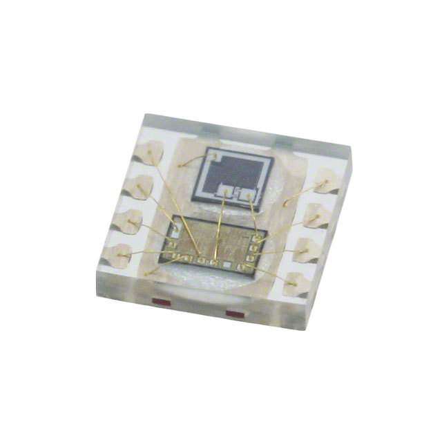
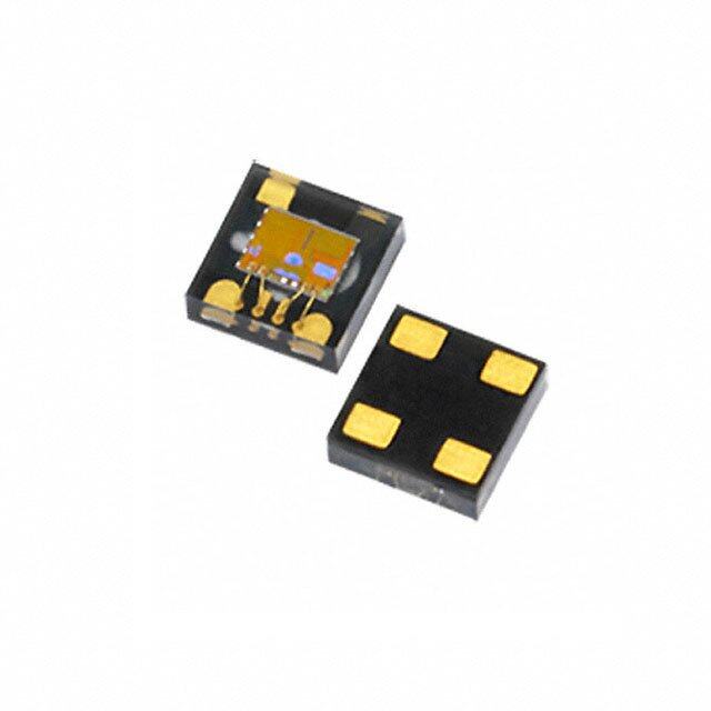
ICGOO电子元器件商城为您提供ML8511-00FCZ05B由ROHM Semiconductor设计生产,在icgoo商城现货销售,并且可以通过原厂、代理商等渠道进行代购。 ML8511-00FCZ05B价格参考。ROHM SemiconductorML8511-00FCZ05B封装/规格:光学传感器 - 环境光,IR,UV 传感器, Optical Sensor Ultraviolet (UV) 365nm Voltage 12-SMD, No Lead。您可以下载ML8511-00FCZ05B参考资料、Datasheet数据手册功能说明书,资料中有ML8511-00FCZ05B 详细功能的应用电路图电压和使用方法及教程。
Rohm Semiconductor的型号ML8511-00FCZ05B是一款UV(紫外线)传感器,属于光学传感器类别下的环境光、IR(红外线)、UV传感器系列。该传感器主要用于检测紫外线强度,并将紫外线辐射转换为电信号输出,广泛应用于以下场景:

 1. 健康与安全设备
   - 紫外线监测仪:用于测量环境中的紫外线强度,帮助用户了解紫外线辐射水平,避免过度暴露对皮肤和眼睛造成的伤害。
   - 防晒提醒设备:集成到可穿戴设备中,提醒用户在紫外线过强时采取防护措施,如涂抹防晒霜或遮阳。

 2. 家用电器
   - 空气净化器:检测紫外线灯的工作状态,确保杀菌功能正常运行。
   - 紫外线消毒设备:用于监控紫外线辐射强度,确保消毒效果达到标准。

 3. 工业应用
   - 紫外线固化设备:在涂料、印刷、电子制造等领域,用于监测紫外线光源的强度,确保固化过程稳定。
   - 环境监测系统:集成到气象站中,实时监测紫外线辐射变化,为科学研究提供数据支持。

 4. 农业与园艺
   - 植物生长灯控制系统:监测紫外线辐射水平,优化植物生长环境,特别是在温室或室内种植场景中。
   - 害虫诱捕设备:通过检测紫外线强度,优化害虫诱捕效率。

 5. 消费电子产品
   - 智能手表/手环:集成紫外线传感器,提供紫外线指数监测功能,增强健康管理能力。
   - 智能手机配件:作为外接模块,扩展手机的环境监测功能。

 特点与优势
- 高灵敏度:能够精确检测紫外线强度,适用于多种应用场景。
- 小型化设计:便于集成到各种便携式设备中。
- 宽工作电压范围:适应不同的电源环境,提升使用灵活性。

总之,ML8511-00FCZ05B凭借其高精度和稳定性,成为紫外线检测领域的理想选择,广泛应用于健康、工业、农业及消费电子等多个领域。
| 参数 | 数值 |
| 产品目录 | |
| 描述 | UV SENSOR W/AMP |
| 产品分类 | |
| 品牌 | Rohm Semiconductor |
| 数据手册 | |
| 产品图片 |
|
| 产品型号 | ML8511-00FCZ05B |
| rohs | 无铅 / 符合限制有害物质指令(RoHS)规范要求 |
| 产品系列 | - |
| 供应商器件封装 | * |
| 其它名称 | ML8511-00FCZ05BDKR |
| 包装 | * |
| 安装类型 | 表面贴装 |
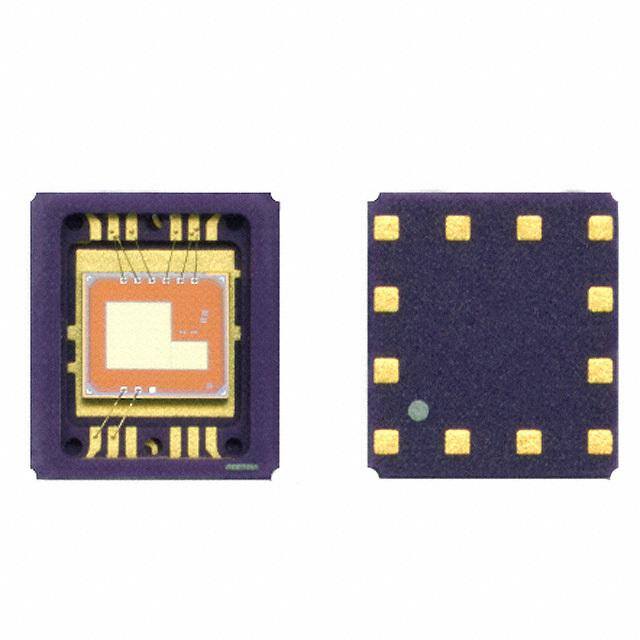
| 封装/外壳 | 12-SMD,扁平引线 |
| 工作温度 | -20°C ~ 70°C |
| 带接近传感器 | 无 |
| 应用说明 | |
| 标准包装 | 1 |
| 波长 | 365nm |
| 电压-电源 | 2.7 V ~ 3.6 V |
| 类型 | UV |
| 输出类型 | 电压 |


- 商务部:美国ITC正式对集成电路等产品启动337调查
- 曝三星4nm工艺存在良率问题 高通将骁龙8 Gen1或转产台积电
- 太阳诱电将投资9.5亿元在常州建新厂生产MLCC 预计2023年完工
- 英特尔发布欧洲新工厂建设计划 深化IDM 2.0 战略
- 台积电先进制程称霸业界 有大客户加持明年业绩稳了
- 达到5530亿美元!SIA预计今年全球半导体销售额将创下新高
- 英特尔拟将自动驾驶子公司Mobileye上市 估值或超500亿美元
- 三星加码芯片和SET,合并消费电子和移动部门,撤换高东真等 CEO
- 三星电子宣布重大人事变动 还合并消费电子和移动部门
- 海关总署:前11个月进口集成电路产品价值2.52万亿元 增长14.8%

PDF Datasheet 数据手册内容提取
FEDL8511-05 Issue Date: March 08, 2013 ML8511 UV Sensor with Voltage Output GENERAL DISCRIPTION The ML8511 is a UV sensor, which is suitable for acquiring UV intensity indoors or outdoors. The ML8511 is equipped with an internal amplifier, which converts photo-current to voltage depending on the UV intensity. This unique feature offers an easy interface to external circuits such as ADC. In the power down mode, typical standby current is 0.1A, thus enabling a longer battery life. FEATURES • Photodiode sensitive to UV-A and UV-B • Embedded operational amplifier • Analog voltage output • Low supply current (300A typ.) and low standby current (0.1A typ.) • Small and thin surface mount package (4.0mm x 3.7mm x 0.73mm, 12-pin ceramic QFN) APPLICATIONS • Smart phone, Watch, Weather station,Bicycle navigation, Accessary, Gaming BLOCK DAIAGRAM TP V EN DD 9 7 4 Amplifier OUT 8 UV Photo- diode ML8511 5 10 GND TR PIN CONFIGURATIONS Pin Symbol I/O Function 7 VDD PW Supply voltage. Decouple this pin to ground with 0.1 F capacitor. 5 GND PW Ground 4 EN I Active high enable pin. (High: Active mode, Low: Standby mode) 8 OUT O Output (Low in power down or standby mode) 9 TP I/O Test pin. Do not connect. 10 TR I/O Internal reference voltage. Decouple this pin to ground with 1 nF capacitor. 1,2,3, 6,11,12 NC - No Connection. Do not connect. 1/8
FEDL8511-05 ML8511 EXAMPLE OF CONNCTING DIAGRAM ML8511 7 VDD 8 OUT ADC 0.1uF 4 EN PORT 5 GND TR 10 1nF * Load resistance of OUT port is recommended more than 100 k. 2/8
FEDL8511-05 ML8511 ABSOLUTE MAXIMUM RATINGS Parameter Symbol Condition Rating unit Supply Voltage V Ta=25 C -0.3 to +4.6 V DD Input Voltage V Ta=25 C -0.3 to +4.6 V I Output Short Current I Ta=25 C 5 mA OS Power Dissipation P Ta=25 C 30 mW D Storage Temperature T - -30 to +85 C stg RECOMENTED OPERATION CONDITIONS Parameter Symbol Min. Typ. Max. unit Operating Voltage V 2.7 3.3 3.6 V DD Operating Temperature Ta -20 - 70 C ELECTRO-OPTICAL CHARACTERISTICS (V =+2.7V to +3.6V, Ta= -20C to +70C) DD Parameter Symbol Condition Min. Typ. Max. unit Supply Current (active mode) I V =V - 300 500 A DDA EN DD Supply Current (standby mode) I V =0 - 0.1 1 A DDS EN Input Voltage (High level) V - V × 0.8 - V + 0.3 V IH DD DD Input Voltage (Low level) V - -0.2 - 0.72 V IL High level input current I V =V - - 1 A IH EN DD Low level input current I V =0 -1 - - A IL EN Wavelength of maximum sensitivity p Ta=25C - 365 - nm Output Setup Time T V =V - - 1 ms SU EN DD Ta=25C, Output Voltage (Shading) * V 0.95 1.0 1.05 V REF V =V EN DD Output Voltage (10mW/cm2 at p) * V Ta=25C, 2.08 2.2 2.32 V O V =V EN DD * Load resistance of OUT port is recommended more than 100 k. 3/8
FEDL8511-05 ML8511 OUTPUT VALTAGE– UV INTENSITY CHARCTERISTICS V =3.0V DD 3.5 3.0 ) V ( e 2.5 g a t l o 2.0 75 ℃ V ut 25 ℃ p 1.5 t u -5 ℃ O 1.0 -25 ℃ 0.5 0 3 6 9 12 15 UV Intensity (mW/cm2) @ λ365nm SPECTRAL RESPONSIVILITY CHARACTERISTICS Ta=25°C, V =3.0V DD 1.0 y 0.8 t vi si n o 0.6 p s e R e 0.4 v i t a el 0.2 R 0.0 280 320 360 400 440 480 520 560 Wavelength (nm) 4/8
FEDL8511-05 ML8511 TIMING CHART Supply voltage and EN signal state should take one of the following procedures: 1. EN should be HIGH or LOW at the same time when V is applied. DD 2. EN should be HIGH or LOW while V is applied. DD Output should be read after output voltage level becomes stable. Maximum time required until stable output voltage reaches is 1 millisecond after EN goes HIGH. V DD EN T SU OUT 5/8
FEDL8511-05 ML8511 PACKAGE DIMENTIONS (Unit: mm) Notes for Mounting the Surface Mount Type Package The surface mount type packages are very susceptible to heat in reflow mounting and humidity absorbed in storage. Therefore, before you perform reflow mounting, contact our responsible sales person for the product name, package name, pin number, package code and desired mounting conditions (reflow method, temperature and times). Specifications are defined without considering the UV absorption by an external cover material. Please contact our sales representativeus when the cover material is applied. Do not press or rub the surface of the resin covering the top of the package where, which is on the UV-ray is light received. In addition, do not apply pressure at high temperature. 6/8
FEDL8511-05 ML8511 REVISON HISTORY Page Document No. Date Previous Current Description Edition Edition FEDL851100FC-01 Sep. 3, 2008 - Preliminary edition FEDL8511-02 Jan. 24, 2008 - 1 Added disclaimer - - Changed Logo OKI to OKI SEMICONDUCTOR The following items has been moved: 1 5 PACKAGE, NOTICE, PRECAUTION and DISCLAIMER. The following items have been moved: 2 1 BLOCK DIAGRAM and PIN CONFIGRATION FEDL8511-03 Nov. 7, 2008 The following tables has been partially modified: 3 2 RECOMMENDED OPERATING CONDITIONS ELECTRO-OPTICAL CHARACTERISTICS 3 2 Changed load resistance 500 k to 100 k - 3 Added graphs - 4 Added “TIMING CHART” Feature description is removed. Applications 1 1 section is added. 4 4 Explanation is provided to the timing chart. FJDL8511-04 Jan. 17, 2013 Package drawing is updated. 5 5 Descriptions in the NOTE are modified. DISCLIMER is removed. 1 1 Descriptions in Pin configurations are modified. FJDL8511-05 Mar. 8, 2013 - 2 Example of connecting diagram is added. 7/8
FEDL8511-05 ML8511 NOTES No copying or reproduction of this document, in part or in whole, is permitted without the consent of LAPIS Semiconductor Co., Ltd. The content specified herein is subject to change for improvement without notice. The content specified herein is for the purpose of introducing LAPIS Semiconductor's products (hereinafter "Products"). If you wish to use any such Product, please be sure to refer to the specifications, which can be obtained from LAPIS Semiconductor upon request. Examples of application circuits, circuit constants and any other information contained herein illustrate the standard usage and operations of the Products. The peripheral conditions must be taken into account when designing circuits for mass production. Great care was taken in ensuring the accuracy of the information specified in this document. However, should you incur any damage arising from any inaccuracy or misprint of such information, LAPIS Semiconductor shall bear no responsibility for such damage. The technical information specified herein is intended only to show the typical functions of and examples of application circuits for the Products. LAPIS Semiconductor does not grant you, explicitly or implicitly, any license to use or exercise intellectual property or other rights held by LAPIS Semiconductor and other parties. LAPIS Semiconductor shall bear no responsibility whatsoever for any dispute arising from the use of such technical information. The Products specified in this document are intended to be used with general-use electronic equipment or devices (such as audio visual equipment, office-automation equipment, communication devices, electronic appliances and amusement devices). The Products specified in this document are not designed to be radiation tolerant. While LAPIS Semiconductor always makes efforts to enhance the quality and reliability of its Products, a Product may fail or malfunction for a variety of reasons. Please be sure to implement in your equipment using the Products safety measures to guard against the possibility of physical injury, fire or any other damage caused in the event of the failure of any Product, such as derating, redundancy, fire control and fail-safe designs. LAPIS Semiconductor shall bear no responsibility whatsoever for your use of any Product outside of the prescribed scope or not in accordance with the instruction manual. The Products are not designed or manufactured to be used with any equipment, device or system which requires an extremely high level of reliability the failure or malfunction of which may result in a direct threat to human life or create a risk of human injury (such as a medical instrument, transportation equipment, aerospace machinery, nuclear-reactor controller, fuel-controller or other safety device). LAPIS Semiconductor shall bear no responsibility in any way for use of any of the Products for the above special purposes. If a Product is intended to be used for any such special purpose, please contact a ROHM sales representative before purchasing. If you intend to export or ship overseas any Product or technology specified herein that may be controlled under the Foreign Exchange and the Foreign Trade Law, you will be required to obtain a license or permit under the Law. Copyright 2008 - 2013 LAPIS Semiconductor Co., Ltd. 8/8