ICGOO在线商城 > 集成电路(IC) > 逻辑 - 缓冲器,驱动器,接收器,收发器 > SN74LVC2G241DCUR
 Datasheet下载
- 型号: SN74LVC2G241DCUR
- 制造商: Texas Instruments
- 库位|库存: xxxx|xxxx
- 要求:
| 数量阶梯 | 香港交货 | 国内含税 |
| +xxxx | $xxxx | ¥xxxx |
查看当月历史价格
查看今年历史价格
SN74LVC2G241DCUR产品简介:
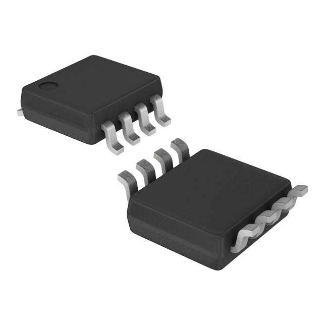
ICGOO电子元器件商城为您提供SN74LVC2G241DCUR由Texas Instruments设计生产,在icgoo商城现货销售,并且可以通过原厂、代理商等渠道进行代购。 SN74LVC2G241DCUR价格参考¥2.04-¥4.64。Texas InstrumentsSN74LVC2G241DCUR封装/规格:逻辑 - 缓冲器,驱动器,接收器,收发器, Buffer, Non-Inverting 2 Element 1 Bit per Element 3-State Output 8-VSSOP。您可以下载SN74LVC2G241DCUR参考资料、Datasheet数据手册功能说明书,资料中有SN74LVC2G241DCUR 详细功能的应用电路图电压和使用方法及教程。
SN74LVC2G241DCUR是Texas Instruments(德州仪器)推出的一款双通道、2位非反相缓冲器/驱动器,属于逻辑 - 缓冲器、驱动器、接收器、收发器类别。该器件采用5引脚SC-70封装,具有低功耗、高速度和宽工作电压范围(1.65V至5.5V)的特点,适用于多种低压数字系统。

典型应用场景包括:

1. 电平转换:由于其支持1.65V至5.5V的宽电压范围,常用于不同电压节点之间的信号电平转换,例如将3.3V系统与5V或1.8V系统进行接口匹配。

2. 信号缓冲与驱动增强:在数字电路中用于增强信号驱动能力,减少信号衰减,提升信号完整性,适用于总线驱动、时钟分配等场景。

3. 便携式设备:因其低功耗和小尺寸封装,广泛应用于智能手机、平板电脑、可穿戴设备等对空间和功耗敏感的电子产品中。

4. 通信接口电路:可用于UART、I²C、GPIO扩展等接口的信号调理与隔离,提高系统稳定性和抗干扰能力。

5. 消费类电子与工业控制:如智能家居模块、传感器接口、小型控制器等,实现信号中继与隔离。

该器件具备三态输出功能,支持高阻抗模式,便于多设备共享总线。同时具有高噪声抑制能力和过压保护(部分引脚),提升了系统可靠性。综合来看,SN74LVC2G241DCUR是一款适用于高性能、低功耗数字系统的理想缓冲驱动器件。
| 参数 | 数值 |
| 产品目录 | 集成电路 (IC)半导体 |
| 描述 | IC BUFF/DVR TRI-ST DL US8缓冲器和线路驱动器 Tri-State Dual |
| 产品分类 | |
| 品牌 | Texas Instruments |
| 产品手册 | |
| 产品图片 |
|
| rohs | 符合RoHS无铅 / 符合限制有害物质指令(RoHS)规范要求 |
| 产品系列 | 逻辑集成电路,缓冲器和线路驱动器,Texas Instruments SN74LVC2G241DCUR74LVC |
| 数据手册 | |
| 产品型号 | SN74LVC2G241DCUR |
| 产品目录页面 | |
| 产品种类 | 缓冲器和线路驱动器 |
| 传播延迟时间 | 4.3 ns at 3.3 V, 3.7 ns at 5 V |
| 低电平输出电流 | 32 mA |
| 供应商器件封装 | US8 |
| 元件数 | 2 |
| 其它名称 | 296-11936-2 |
| 包装 | 带卷 (TR) |
| 单位重量 | 9.600 mg |
| 商标 | Texas Instruments |
| 安装类型 | 表面贴装 |
| 安装风格 | SMD/SMT |
| 封装 | Reel |
| 封装/外壳 | 8-VFSOP(0.091",2.30mm 宽) |
| 封装/箱体 | VSSOP-8 |
| 工作温度 | -40°C ~ 125°C |
| 工厂包装数量 | 3000 |
| 最大工作温度 | + 85 C |
| 最小工作温度 | - 40 C |
| 极性 | Non-Inverting |
| 标准包装 | 3,000 |
| 每元件位数 | 1 |
| 每芯片的通道数量 | 2 |
| 电压-电源 | 1.65 V ~ 5.5 V |
| 电流-输出高,低 | 32mA,32mA |
| 电源电压-最大 | 5.5 V |
| 电源电压-最小 | 1.65 V |
| 系列 | SN74LVC2G241 |
| 输入线路数量 | 2 |
| 输出类型 | 3-State |
| 输出线路数量 | 2 |
| 逻辑类型 | 缓冲器/线路驱动器,非反相 |
| 逻辑系列 | LVC |
| 高电平输出电流 | - 32 mA |


- 商务部:美国ITC正式对集成电路等产品启动337调查
- 曝三星4nm工艺存在良率问题 高通将骁龙8 Gen1或转产台积电
- 太阳诱电将投资9.5亿元在常州建新厂生产MLCC 预计2023年完工
- 英特尔发布欧洲新工厂建设计划 深化IDM 2.0 战略
- 台积电先进制程称霸业界 有大客户加持明年业绩稳了
- 达到5530亿美元!SIA预计今年全球半导体销售额将创下新高
- 英特尔拟将自动驾驶子公司Mobileye上市 估值或超500亿美元
- 三星加码芯片和SET,合并消费电子和移动部门,撤换高东真等 CEO
- 三星电子宣布重大人事变动 还合并消费电子和移动部门
- 海关总署:前11个月进口集成电路产品价值2.52万亿元 增长14.8%


PDF Datasheet 数据手册内容提取
Product Order Technical Tools & Support & Folder Now Documents Software Community SN74LVC2G241 SCES210P–APRIL1999–REVISEDJANUARY2019 SN74LVC2G241 Dual Buffer and Driver With 3-State Outputs 1 Features 3 Description • AvailableintheTexasInstruments This dual buffer and line driver is designed for 1.65-V 1 to5.5-VV operation. NanoFree™Package CC • Supports5-VV Operation The SN74LVC2G241 device is designed specifically CC to improve both the performance and density of 3- • InputsAcceptVoltagesto5.5V state memory-address drivers, clock drivers, and bus- • Maxt of4.1nsat3.3V pd orientedreceiversandtransmitters. • LowPowerConsumption,10-µAMaximumI CC NanoFree package technology is a major • ±24-mAOutputDriveat3.3V breakthrough in IC packaging concepts, using the die • TypicalV (OutputGroundBounce) asthepackage. OLP <0.8VatV =3.3V,T =25°C CC A The SN74LVC2G241 device is organized as two 1-bit • TypicalV (OutputV Undershoot) line drivers with separate output-enable (1OE, 2OE) OHV OH >2VatV =3.3V,T =25°C inputs. When 1OE is low and 2OE is high, the device CC A • I SupportsLiveInsertion,Partial-Power-Down passes data from the A inputs to the Y outputs. When off 1OE is high and 2OE is low, the outputs are in the Mode,andBack-DriveProtection high-impedancestate. • CanBeUsedasaDownTranslatortoTranslate InputsFromaMaxof5.5VDown To ensure the high-impedance state during power up or power down, OE should be tied to V through a totheV Level CC CC pullup resistor, and OE should be tied to GND • Latch-UpPerformanceExceeds100mAPer through a pulldown resistor; the minimum value of the JESD78,ClassII resistor is determined by the current-sinking or the • ESDProtectionExceedsJESD22 current-sourcingcapabilityofthedriver. – 2000-VHuman-BodyModel(A114-A) This device is fully specified for partial-power-down – 200-VMachineModel(A115-A) applications using I . The I circuitry disables the off off outputs, preventing damaging current backflow – 1000-VCharged-DeviceModel(C101) throughthedevicewhenitispowereddown. 2 Applications DeviceInformation(1) • AVReceivers PARTNUMBER PACKAGE BODYSIZE(NOM) • Blu-rayPlayersandHomeTheaters SN74LVC2G241DCT SM8(8) 2.95mm×2.80mm • DVDRecordersandPlayers SN74LVC2G241DCU VSOOP(8) 2.30mm×2.00mm • DesktoporNotebookPCs SN74LVC2G241YZP DSBGA(8) 1.91mm×0.91mm • DigitalRadioorInternetRadioPlayers (1) For all available packages, see the orderable addendum at theendofthedatasheet. • DigitalVideoCameras(DVC) • EmbeddedPCs LogicDiagram(PositiveLogic) • GPS:PersonalNavigationDevices 1 • MobileInternetDevices 1OE • NetworkProjectorFront-Ends 2 6 1A 1Y • PortableMediaPlayers • ProAudioMixers 7 2OE 5 3 2A 2Y 1 An IMPORTANT NOTICE at the end of this data sheet addresses availability, warranty, changes, use in safety-critical applications, intellectualpropertymattersandotherimportantdisclaimers.PRODUCTIONDATA.
SN74LVC2G241 SCES210P–APRIL1999–REVISEDJANUARY2019 www.ti.com Table of Contents 1 Features.................................................................. 1 8.2 FunctionalBlockDiagram.........................................8 2 Applications........................................................... 1 8.3 FeatureDescription...................................................8 3 Description............................................................. 1 8.4 DeviceFunctionalModes..........................................8 4 RevisionHistory..................................................... 2 9 ApplicationandImplementation.......................... 9 9.1 ApplicationInformation..............................................9 5 PinConfigurationandFunctions......................... 3 9.2 TypicalApplication ...................................................9 6 Specifications......................................................... 4 10 PowerSupplyRecommendations..................... 10 6.1 AbsoluteMaximumRatings .....................................4 11 Layout................................................................... 10 6.2 ESDRatings..............................................................4 6.3 RecommendedOperatingConditions......................4 11.1 LayoutGuidelines.................................................10 6.4 ThermalInformation..................................................5 11.2 LayoutExample....................................................10 6.5 ElectricalCharacteristics...........................................5 12 DeviceandDocumentationSupport................. 11 6.6 SwitchingCharacteristics..........................................6 12.1 DocumentationSupport........................................11 6.7 OperatingCharacteristics..........................................6 12.2 CommunityResources..........................................11 6.8 TypicalCharacteristic................................................6 12.3 Trademarks...........................................................11 7 ParameterMeasurementInformation..................7 12.4 ElectrostaticDischargeCaution............................11 12.5 Glossary................................................................11 8 DetailedDescription.............................................. 8 13 Mechanical,Packaging,andOrderable 8.1 Overview...................................................................8 Information........................................................... 11 4 Revision History NOTE:Pagenumbersforpreviousrevisionsmaydifferfrompagenumbersinthecurrentversion. ChangesfromRevisionO(December2015)toRevisionP Page • ChangedElectricalCharacteristicstableformat ................................................................................................................... 5 • ChangedSwitchingCharacteristicstablesformat. ................................................................................................................ 6 ChangesfromRevisionN(November2013)toRevisionO Page • AddedApplicationssection,DeviceInformationtable,ESDRatingstable,ThermalInformationtable,Typical Characteristics,FeatureDescriptionsection,DeviceFunctionalModes,ApplicationandImplementationsection, PowerSupplyRecommendationssection,Layoutsection,DeviceandDocumentationSupportsection,and Mechanical,Packaging,andOrderableInformationsection.................................................................................................. 1 ChangesfromRevisionM(February2007)toRevisionN Page • UpdateddocumenttonewTIdatasheetformat.................................................................................................................... 1 • RemovedOrderingInformationtable..................................................................................................................................... 1 • UpdatedFeatures................................................................................................................................................................... 1 • Updatedoperatingtemperaturerange................................................................................................................................... 4 2 SubmitDocumentationFeedback Copyright©1999–2019,TexasInstrumentsIncorporated ProductFolderLinks:SN74LVC2G241
SN74LVC2G241 www.ti.com SCES210P–APRIL1999–REVISEDJANUARY2019 5 Pin Configuration and Functions DCTPackage 8-PinSM8 DCUPackage TopView 8-PinVSSOP TopView 1OE 1 8 VCC 1OE 1 8 VCC 1A 2 7 2OE 1A 2 7 2OE 2Y 3 6 1Y 2Y 3 6 1Y GND 4 5 2A GND 4 5 2A YZPPackage 8-PinDSBGA BottomView GND 45 2A 2Y 36 1Y 1A 27 2OE 1OE 18 VCC PinFunctions(1)(2) PIN I/O DESCRIPTION NAME NO. 1A 2 I Input 1OE 1 I Outputenable(Activelow) 1Y 6 O Output 2A 5 I Input 2Y 3 O Output 2OE 7 I Outputenable(Activehigh) GND 4 — Ground V 8 — Powerpin CC (1) N.C.–Nointernalconnection (2) Seefordimensions Copyright©1999–2019,TexasInstrumentsIncorporated SubmitDocumentationFeedback 3 ProductFolderLinks:SN74LVC2G241
SN74LVC2G241 SCES210P–APRIL1999–REVISEDJANUARY2019 www.ti.com 6 Specifications 6.1 Absolute Maximum Ratings overoperatingfree-airtemperaturerange(unlessotherwisenoted)(1) MIN MAX UNIT V Supplyvoltage –0.5 6.5 V CC V Inputvoltage(2) –0.5 6.5 V I V Voltageappliedtoanyoutputinthehigh-impedanceorpower-offstate(2) –0.5 6.5 V O V Voltageappliedtoanyoutputinthehighorlowstate(2)(3) –0.5 V +0.5 V O CC I Inputclampcurrent V <0 –50 mA IK I I Outputclampcurrent V <0 –50 mA OK O I Continuousoutputcurrent ±50 mA O ContinuouscurrentthroughV orGND ±100 mA CC T Maximumjunctiontemperature 150 °C J T Storagetemperature –65 150 °C stg (1) StressesbeyondthoselistedunderAbsoluteMaximumRatingsmaycausepermanentdamagetothedevice.Thesearestressratings only,andfunctionaloperationofthedeviceattheseoranyotherconditionsbeyondthoseindicatedunderRecommendedOperating Conditionsisnotimplied.Exposuretoabsolute-maximum-ratedconditionsforextendedperiodsmayaffectdevicereliability. (2) Theinputnegative-voltageandoutputvoltageratingsmaybeexceedediftheinputandoutputcurrentratingsareobserved. (3) ThevalueofV isprovidedintheRecommendedOperatingConditionstable. CC 6.2 ESD Ratings VALUE UNIT Human-bodymodel(HBM),perANSI/ESDA/JEDECJS-001,allpins(1) ±2000 Electrostatic V(ESD) discharge Cpihnasr(g2)ed-devicemodel(CDM),perJEDECspecificationJESD22-C101,all ±1000 V (1) JEDECdocumentJEP155statesthat500-VHBMallowssafemanufacturingwithastandardESDcontrolprocess. (2) JEDECdocumentJEP157statesthat250-VCDMallowssafemanufacturingwithastandardESDcontrolprocess. 6.3 Recommended Operating Conditions(1) MIN MAX UNIT Operating 1.65 5.5 V Supplyvoltage V CC Dataretentiononly 1.5 V =1.65Vto1.95V 0.65×V CC CC V =2.3Vto2.7V 1.7 CC V High-levelinputvoltage V IH V =3Vto3.6V 2 CC V =4.5Vto5.5V 0.7×V CC CC V =1.65Vto1.95V 0.35×V CC CC V =2.3Vto2.7V 0.7 CC V Low-levelinputvoltage V IL V =3Vto3.6V 0.8 CC V =4.5Vto5.5V 0.3×V CC CC V Inputvoltage 0 5.5 V I Highorlowstate 0 V CC V Outputvoltage V O 3-state 0 5.5 V =1.65V –4 CC V =2.3V –8 CC I High-leveloutputcurrent –16 mA OH V =3V CC –24 V =4.5V –32 CC (1) AllunusedinputsofthedevicemustbeheldatV orGNDtoensureproperdeviceoperation.RefertotheTIapplicationreport CC ImplicationsofSloworFloatingCMOSInputs,SCBA004. 4 SubmitDocumentationFeedback Copyright©1999–2019,TexasInstrumentsIncorporated ProductFolderLinks:SN74LVC2G241
SN74LVC2G241 www.ti.com SCES210P–APRIL1999–REVISEDJANUARY2019 Recommended Operating Conditions(1) (continued) MIN MAX UNIT V =1.65V 4 CC V =2.3V 8 CC I Low-leveloutputcurrent 16 mA OL V =3V CC 24 V =4.5V 32 CC V =1.8V±0.15V,2.5V±0.2V 20 CC Δt/Δv Inputtransitionriseorfallrate V =3.3V±0.3V 10 ns/V CC V =5V±0.5V 5 CC T Operatingfree-airtemperature –40 85 °C A 6.4 Thermal Information SN74LVC2G241 THERMALMETRIC(1) DCT DCU YZP UNIT (SM8) (VSSOP) (DSBGA) 8PINS 8PINS 8PINS R Junction-to-ambientthermalresistance 220 227 102 °C/W θJA (1) Formoreinformationabouttraditionalandnewthermalmetrics,seetheSemiconductorandICPackageThermalMetricsapplication report,SPRA953. 6.5 Electrical Characteristics overrecommendedoperatingfree-airtemperaturerange,T =–40ºCto125°C(unlessotherwisenoted) A –40°Cto125°C –40°Cto85°C PARAMETER TESTCONDITIONS VCC (Recommended) UNIT MIN TYP MAX MIN TYP MAX IOH=–100µA 1.65Vto5.5V VCC –0.1 VCC –0.1 IOH=–4mA 1.65V 1.2 1.2 IOH=–8mA 2.3V 1.9 1.9 VOH V IOH=–16mA 2.4 2.4 3V IOH=–24mA 2.3 2.3 IOH=–32mA 4.5V 3.8 3.8 IOL=100µA 1.65Vto5.5V 0.1 0.1 IOL=4mA 1.65V 0.45 0.45 IOL=8mA 2.3V 0.3 0.3 VOL V IOL=16mA 0.4 0.4 3V IOL=24mA 0.55 0.55 IOL=32mA 4.5V 0.55 0.75 AorOE II inputs VI=5.5VorGND 0to5.5V ±5 ±5 µA Ioff VIorVO=5.5V 0 ±10 ±10 µA IOZ VO=0to5.5V 3.6V 10 10 µA ICC VI=5.5VorGND, IO=0 1.65Vto5.5V 10 10 µA ΔICC OOntheerinipnuptuatstaVtCVCCC–o0r.6GVN,D 3Vto5.5V 500 500 µA DataInputs 3.5 Ci VI=VCCorGND 3.3V pF ControlInputs 4 Co VO=VCCorGND 3.3V 6.5 pF Copyright©1999–2019,TexasInstrumentsIncorporated SubmitDocumentationFeedback 5 ProductFolderLinks:SN74LVC2G241
SN74LVC2G241 SCES210P–APRIL1999–REVISEDJANUARY2019 www.ti.com 6.6 Switching Characteristics overrecommendedoperatingfree-airtemperaturerange(unlessotherwisenoted)(seeFigure2) –40°Cto85°C PARAMETER FROM TO VCC=1.8V VCC=2.5V VCC=3.3V VCC=5V UNIT (INPUT) (OUTPUT) ±0.15V ±0.2V ±0.3V ±0.5V MIN MAX MIN MAX MIN MAX MIN MAX tpd A Y 3.3 9.1 1.5 5.5 1.4 4.3 1.0 4.0 ns ten OE Y 4.0 9.9 1.3 6.6 1.2 4.7 1.1 5.0 ns tdis OE Y 1.5 11.6 1.0 5.7 1.4 4.6 0.5 4.2 ns –40°Cto125°C(Recommended) PARAMETER FROM TO VCC=1.8V VCC=2.5V VCC=3.3V VCC=5V UNIT (INPUT) (OUTPUT) ±0.15V ±0.2V ±0.3V ±0.5V MIN MAX MIN MAX MIN MAX MIN MAX tpd A Y 3.3 10.1 1.5 5.6 1.4 5.3 1.0 4.2 ns ten OE Y 4.0 10.9 1.3 6.6 1.2 5.7 1.2 4.3 ns tdis OE Y 1.5 12.6 1.0 6.6 1.4 5.6 1.0 3.9 ns 6.7 Operating Characteristics T =25°C A PARAMETER TESTCONDITIONS V TYP UNIT CC V =1.8V 19 CC V =2.5V 19 CC Outputsenabled pF V =3.3V 20 CC Powerdissipation V =5V 22 CC C capacitance f=10MHz pd perbuffer/driver VCC=1.8V 2 V =2.5V 2 CC Outputsdisabled pF V =3.3V 2 CC V =5V 3 CC 6.8 Typical Characteristic 3.5 3 2.5 ) D P y (t a 2 el D n o ati 1.5 g a p o Pr 1 0.5 Typ. Char. 0 0 1 2 3 4 5 6 Supply Voltage [V ] (V) CC C001 Figure1.tpdvsVccOverFullTemperatureRange 6 SubmitDocumentationFeedback Copyright©1999–2019,TexasInstrumentsIncorporated ProductFolderLinks:SN74LVC2G241
SN74LVC2G241 www.ti.com SCES210P–APRIL1999–REVISEDJANUARY2019 7 Parameter Measurement Information V LOAD R S1 Open From Output L TEST S1 Under Test GND t /t Open C PLH PHL (see NoteA)L RL tPLZ/tPZL VLOAD t /t GND PHZ PZH LOAD CIRCUIT INPUTS V V V C R V CC V t/t M LOAD L L D I r f 1.8 V±0.15 V V £2 ns V /2 2 ×V 30 pF 1 kW 0.15 V CC CC CC 2.5 V±0.2 V V £2 ns V /2 2 ×V 30 pF 500W 0.15 V CC CC CC 3.3 V±0.3 V 3 V £2.5 ns 1.5 V 6 V 50 pF 500W 0.3 V 5 V±0.5 V V £2.5 ns V /2 2 ×V 50 pF 500W 0.3 V CC CC CC V I Timing Input V M 0 V t W VI tsu th V Input V V I M M Data Input V V M M 0 V 0 V VOLTAGE WAVEFORMS VOLTAGE WAVEFORMS PULSE DURATION SETUPAND HOLD TIMES Input VM VM VI COounttpruotl VM VM VI 0 V 0 V t t t t PLH PHL PZL PLZ V Output V /2 Output VM VM OH WSav1e afot rVm 1 VM V + V LOAD VOL (see NoteL OBAD) OL D VOL t t PHL PLH t t PZH PHZ Output VM VM VOH WSa1v eaOfto uGrtmpNu D2t VM VOH–VD VOH VOL (see Note B) »0 V VOLTAGE WAVEFORMS VOLTAGE WAVEFORMS PROPAGATION DELAYTIMES ENABLEAND DISABLE TIMES INVERTINGAND NONINVERTING OUTPUTS LOW-AND HIGH-LEVELENABLING NOTES: A. C includes probe and jig capacitance. L B. Waveform 1 is for an output with internal conditions such that the output is low, except when disabled by the output control. Waveform 2 is for an output with internal conditions such that the output is high, except when disabled by the output control. C. All input pulses are supplied by generators having the following characteristics: PRR£10 MHz, Z = 50W. O D. The outputs are measured one at a time, with one transition per measurement. E. t and t are the same as t . PLZ PHZ dis F. t and t are the same as t . PZL PZH en G.t and t are the same as t . PLH PHL pd H. All parameters and waveforms are not applicable to all devices. Figure2. LoadCircuitandVoltageWaveforms Copyright©1999–2019,TexasInstrumentsIncorporated SubmitDocumentationFeedback 7 ProductFolderLinks:SN74LVC2G241
SN74LVC2G241 SCES210P–APRIL1999–REVISEDJANUARY2019 www.ti.com 8 Detailed Description 8.1 Overview The SN74LVC2G241 device is designed specifically to improve both the performance and density of 3-state memory-address drivers, clock drivers, and bus-oriented receivers and transmitters. The SN74LVC2G241 device is organized as two 1-bit line drivers with separate output-enable (1OE, 2OE) inputs. When 1OE is low and 2OE is high, the device passes data from the A inputs to the Y outputs. When 1OE is high and 2OE is low, the outputsareinthehigh-impedancestate. TheSN74LVC2G241isalsoaneffectiveredriver,withamaximumoutputcurrentdriveof32mA. 8.2 Functional Block Diagram 1 1OE 2 6 1A 1Y 7 2OE 5 3 2A 2Y Figure3. LogicDiagram(PositiveLogic) 8.3 Feature Description To ensure the high-impedance state during power up or power down, OE should be tied to V through a pullup CC resistor, and OE should be tied to GND through a pulldown resistor; the minimum value of the resistor is determinedbythecurrent-sinkingorthecurrent-sourcingcapabilityofthedriver. This device is fully specified for partial-power-down applications using I . The I circuitry disables the outputs, off off preventingdamagingcurrentbackflowthroughthedevicewhenitispowereddown. 8.4 Device Functional Modes Table1andTable2listthefunctionalmodesoftheSN74LVC2G241. Table1.Gate1FunctionalTable INPUTS OUTPUT 1OE 1A 1Y L H H L L L H X Z Table2.Gate2FunctionalTable INPUTS OUTPUT 2OE 2A 2Y H H H H L L L X Z 8 SubmitDocumentationFeedback Copyright©1999–2019,TexasInstrumentsIncorporated ProductFolderLinks:SN74LVC2G241
SN74LVC2G241 www.ti.com SCES210P–APRIL1999–REVISEDJANUARY2019 9 Application and Implementation NOTE Information in the following applications sections is not part of the TI component specification, and TI does not warrant its accuracy or completeness. TI’s customers are responsible for determining suitability of components for their purposes. Customers should validateandtesttheirdesignimplementationtoconfirmsystemfunctionality. 9.1 Application Information Typical Application shows a simple application where a physical push button is connected to the SN74LVC2G241. The push button is in a physical location far enough away from the processor that the input signal is weak and needs to be redriven. The SN74LVC2G241 acts as a redriver, providing a strong input signal totheprocessorwithaslittleas1nsofpropagationdelay. 9.2 Typical Application V CC Physical Push Button Microprocessor SN74LVC2G241 (One driver) Figure4. SN74LVC2G241Application 9.2.1 DesignRequirements ThisdeviceusesCMOStechnologyandhasbalancedoutputdrive.Takecaretoavoidbuscontentionbecauseit can drive currents that would exceed maximum limits. The high drive also creates fast edges into light loads, so routingandloadconditionsmustbeconsideredtopreventringing. 9.2.2 DetailedDesignProcedure 1. RecommendedInputConditions – Risetimeandfalltimespecs.See(Δt/ΔV)inRecommendedOperatingConditions. – Specifiedhighandlowlevels.See(V andV )inRecommendedOperatingConditions. IH IL – Inputs are overvoltage tolerant allowing them to go as high as (V max) in Recommended Operating I ConditionsatanyvalidV . CC 2. RecommendOutputConditions – Loadcurrentsmustnotexceed(I max)peroutputandmustnotexceed(ContinuouscurrentthroughV O CC orGND)totalcurrentforthepart.TheselimitsarelocatedinAbsoluteMaximumRatings. – OutputsmustnotbepulledaboveV duringnormaloperationor5.5Vinhigh-zstate. CC Copyright©1999–2019,TexasInstrumentsIncorporated SubmitDocumentationFeedback 9 ProductFolderLinks:SN74LVC2G241
SN74LVC2G241 SCES210P–APRIL1999–REVISEDJANUARY2019 www.ti.com Typical Application (continued) 9.2.3 ApplicationCurve 1600 Icc 1.8V 1400 Icc 2.5V Icc 3.3V 1200 Icc 5V 1000 A µ c - 800 c I 600 400 200 0 0 20 40 60 80 Frequency - MHz D001 Figure5. I vsFrequency CC 10 Power Supply Recommendations The power supply can be any voltage between the minimum and maximum supply voltage rating located in RecommendedOperatingConditions. Each V pin should have a good bypass capacitor to prevent power disturbance. For devices with a single CC supply, a 0.1-μF capacitor is recommended and if there are multiple V pins then a 0.01-μF or 0.022-μF CC capacitor is recommended for each power pin. It is ok to parallel multiple bypass capacitors to reject different frequencies of noise. 0.1-μF and 1-μF capacitors are commonly used in parallel. The bypass capacitor should be installedasclosetothepowerpinaspossibleforbestresults. 11 Layout 11.1 Layout Guidelines When using multiple bit logic devices inputs must not ever float. In many cases, functions or parts of functions of digital logic devices are unused; for example, when only two inputs of a triple-input AND gate are used or only 3 of the 4 buffer gates are used. Such input pins must not be left unconnected because the undefined voltages at the outside connections result in undefined operational states. Specified below are the rules that must be observed under all circumstances. All unused inputs of digital logic devices must be connected to a high or low bias to prevent them from floating. The logic level that should be applied to any particular unused input depends on the function of the device. Generally they will be tied to GND or V , whichever make more sense or is more CC convenient. 11.2 Layout Example VCC Input Unused Input Output Unused Input Output Input Figure6. LayoutDiagram 10 SubmitDocumentationFeedback Copyright©1999–2019,TexasInstrumentsIncorporated ProductFolderLinks:SN74LVC2G241
SN74LVC2G241 www.ti.com SCES210P–APRIL1999–REVISEDJANUARY2019 12 Device and Documentation Support 12.1 Documentation Support 12.1.1 RelatedDocumentation Forrelateddocumentation,seethefollowing: ImplicationsofSloworFloatingCMOSInputs,SCBA004 12.2 Community Resources The following links connect to TI community resources. Linked contents are provided "AS IS" by the respective contributors. They do not constitute TI specifications and do not necessarily reflect TI's views; see TI's Terms of Use. TIE2E™OnlineCommunity TI'sEngineer-to-Engineer(E2E)Community.Createdtofostercollaboration amongengineers.Ate2e.ti.com,youcanaskquestions,shareknowledge,exploreideasandhelp solveproblemswithfellowengineers. DesignSupport TI'sDesignSupport QuicklyfindhelpfulE2Eforumsalongwithdesignsupporttoolsand contactinformationfortechnicalsupport. 12.3 Trademarks NanoFree,E2EaretrademarksofTexasInstruments. Allothertrademarksarethepropertyoftheirrespectiveowners. 12.4 Electrostatic Discharge Caution Thesedeviceshavelimitedbuilt-inESDprotection.Theleadsshouldbeshortedtogetherorthedeviceplacedinconductivefoam duringstorageorhandlingtopreventelectrostaticdamagetotheMOSgates. 12.5 Glossary SLYZ022—TIGlossary. Thisglossarylistsandexplainsterms,acronyms,anddefinitions. 13 Mechanical, Packaging, and Orderable Information The following pages include mechanical packaging and orderable information. This information is the most current data available for the designated devices. This data is subject to change without notice and revision of thisdocument.Forbrowserbasedversionsofthisdatasheet,refertothelefthandnavigation. Copyright©1999–2019,TexasInstrumentsIncorporated SubmitDocumentationFeedback 11 ProductFolderLinks:SN74LVC2G241
PACKAGE OPTION ADDENDUM www.ti.com 6-Feb-2020 PACKAGING INFORMATION Orderable Device Status Package Type Package Pins Package Eco Plan Lead/Ball Finish MSL Peak Temp Op Temp (°C) Device Marking Samples (1) Drawing Qty (2) (6) (3) (4/5) 74LVC2G241DCTRE4 ACTIVE SM8 DCT 8 3000 Green (RoHS NIPDAU Level-1-260C-UNLIM -40 to 125 C41 & no Sb/Br) Z 74LVC2G241DCTRG4 ACTIVE SM8 DCT 8 3000 Green (RoHS NIPDAU Level-1-260C-UNLIM -40 to 125 C41 & no Sb/Br) Z 74LVC2G241DCUTG4 ACTIVE VSSOP DCU 8 250 Green (RoHS NIPDAU Level-1-260C-UNLIM -40 to 125 C41R & no Sb/Br) SN74LVC2G241DCTR ACTIVE SM8 DCT 8 3000 Green (RoHS NIPDAU Level-1-260C-UNLIM -40 to 125 C41 & no Sb/Br) Z SN74LVC2G241DCUR ACTIVE VSSOP DCU 8 3000 Green (RoHS NIPDAU | SN Level-1-260C-UNLIM -40 to 125 (C41Q, C41R) & no Sb/Br) SN74LVC2G241DCUT ACTIVE VSSOP DCU 8 250 Green (RoHS NIPDAU | SN Level-1-260C-UNLIM -40 to 125 (C41Q, C41R) & no Sb/Br) SN74LVC2G241YZPR ACTIVE DSBGA YZP 8 3000 Green (RoHS SNAGCU Level-1-260C-UNLIM -40 to 125 (C2, C27) & no Sb/Br) (1) The marketing status values are defined as follows: ACTIVE: Product device recommended for new designs. LIFEBUY: TI has announced that the device will be discontinued, and a lifetime-buy period is in effect. NRND: Not recommended for new designs. Device is in production to support existing customers, but TI does not recommend using this part in a new design. PREVIEW: Device has been announced but is not in production. Samples may or may not be available. OBSOLETE: TI has discontinued the production of the device. (2) RoHS: TI defines "RoHS" to mean semiconductor products that are compliant with the current EU RoHS requirements for all 10 RoHS substances, including the requirement that RoHS substance do not exceed 0.1% by weight in homogeneous materials. Where designed to be soldered at high temperatures, "RoHS" products are suitable for use in specified lead-free processes. TI may reference these types of products as "Pb-Free". RoHS Exempt: TI defines "RoHS Exempt" to mean products that contain lead but are compliant with EU RoHS pursuant to a specific EU RoHS exemption. Green: TI defines "Green" to mean the content of Chlorine (Cl) and Bromine (Br) based flame retardants meet JS709B low halogen requirements of <=1000ppm threshold. Antimony trioxide based flame retardants must also meet the <=1000ppm threshold requirement. (3) MSL, Peak Temp. - The Moisture Sensitivity Level rating according to the JEDEC industry standard classifications, and peak solder temperature. (4) There may be additional marking, which relates to the logo, the lot trace code information, or the environmental category on the device. (5) Multiple Device Markings will be inside parentheses. Only one Device Marking contained in parentheses and separated by a "~" will appear on a device. If a line is indented then it is a continuation of the previous line and the two combined represent the entire Device Marking for that device. Addendum-Page 1
PACKAGE OPTION ADDENDUM www.ti.com 6-Feb-2020 (6) Lead/Ball Finish - Orderable Devices may have multiple material finish options. Finish options are separated by a vertical ruled line. Lead/Ball Finish values may wrap to two lines if the finish value exceeds the maximum column width. Important Information and Disclaimer:The information provided on this page represents TI's knowledge and belief as of the date that it is provided. TI bases its knowledge and belief on information provided by third parties, and makes no representation or warranty as to the accuracy of such information. Efforts are underway to better integrate information from third parties. TI has taken and continues to take reasonable steps to provide representative and accurate information but may not have conducted destructive testing or chemical analysis on incoming materials and chemicals. TI and TI suppliers consider certain information to be proprietary, and thus CAS numbers and other limited information may not be available for release. In no event shall TI's liability arising out of such information exceed the total purchase price of the TI part(s) at issue in this document sold by TI to Customer on an annual basis. Addendum-Page 2
PACKAGE MATERIALS INFORMATION www.ti.com 17-Apr-2020 TAPE AND REEL INFORMATION *Alldimensionsarenominal Device Package Package Pins SPQ Reel Reel A0 B0 K0 P1 W Pin1 Type Drawing Diameter Width (mm) (mm) (mm) (mm) (mm) Quadrant (mm) W1(mm) 74LVC2G241DCUTG4 VSSOP DCU 8 250 180.0 8.4 2.25 3.35 1.05 4.0 8.0 Q3 SN74LVC2G241DCTR SM8 DCT 8 3000 180.0 13.0 3.35 4.5 1.55 4.0 12.0 Q3 SN74LVC2G241DCUR VSSOP DCU 8 3000 180.0 8.4 2.25 3.35 1.05 4.0 8.0 Q3 SN74LVC2G241DCUR VSSOP DCU 8 3000 178.0 9.5 2.25 3.35 1.05 4.0 8.0 Q3 SN74LVC2G241DCUT VSSOP DCU 8 250 178.0 9.5 2.25 3.35 1.05 4.0 8.0 Q3 SN74LVC2G241YZPR DSBGA YZP 8 3000 180.0 8.4 1.02 2.02 0.63 4.0 8.0 Q1 PackMaterials-Page1
PACKAGE MATERIALS INFORMATION www.ti.com 17-Apr-2020 *Alldimensionsarenominal Device PackageType PackageDrawing Pins SPQ Length(mm) Width(mm) Height(mm) 74LVC2G241DCUTG4 VSSOP DCU 8 250 202.0 201.0 28.0 SN74LVC2G241DCTR SM8 DCT 8 3000 182.0 182.0 20.0 SN74LVC2G241DCUR VSSOP DCU 8 3000 202.0 201.0 28.0 SN74LVC2G241DCUR VSSOP DCU 8 3000 202.0 201.0 28.0 SN74LVC2G241DCUT VSSOP DCU 8 250 202.0 201.0 28.0 SN74LVC2G241YZPR DSBGA YZP 8 3000 182.0 182.0 20.0 PackMaterials-Page2
MECHANICAL DATA MPDS049B – MAY 1999 – REVISED OCTOBER 2002 DCT (R-PDSO-G8) PLASTIC SMALL-OUTLINE PACKAGE 0,30 0,65 0,13 M 0,15 8 5 0,15 NOM 2,90 4,25 ÇÇÇÇÇ 2,70 3,75 ÇÇÇÇÇ ÇÇÇÇÇ Gage Plane ÇÇÇÇÇ PIN 1 INDEX AREA 0,25 1 4 0°– 8° 3,15 0,60 2,75 0,20 1,30 MAX Seating Plane 0,10 0,10 0,00 4188781/C 09/02 NOTES: A. All linear dimensions are in millimeters. B. This drawing is subject to change without notice. C. Body dimensions do not include mold flash or protrusion D. Falls within JEDEC MO-187 variation DA. • POST OFFICE BOX 655303 DALLAS, TEXAS 75265
None
PACKAGE OUTLINE YZP0008 DSBGA - 0.5 mm max height SCALE 8.000 DIE SIZE BALL GRID ARRAY B E A BALL A1 CORNER D C 0.5 MAX SEATING PLANE 0.19 0.05 C 0.15 BALL TYP 0.5 TYP D C SYMM 1.5 D: Max = 1.918 mm, Min =1 .858 mm TYP B E: Max = 0.918 mm, Min =0 .858 mm 0.5 TYP A 0.25 8X 1 2 0.21 0.015 C A B SYMM 4223082/A 07/2016 NOTES: 1. All linear dimensions are in millimeters. Any dimensions in parenthesis are for reference only. Dimensioning and tolerancing per ASME Y14.5M. 2. This drawing is subject to change without notice. www.ti.com
EXAMPLE BOARD LAYOUT YZP0008 DSBGA - 0.5 mm max height DIE SIZE BALL GRID ARRAY (0.5) TYP 8X ( 0.23) 1 2 A (0.5) TYP B SYMM C D SYMM LAND PATTERN EXAMPLE SCALE:40X SOLDER MASK 0.05 MAX 0.05 MIN ( 0.23) OPENING SOLDER MASK OPENING ( 0.23) METAL METAL UNDER SOLDER MASK NON-SOLDER MASK SOLDER MASK DEFINED DEFINED (PREFERRED) SOLDER MASK DETAILS NOT TO SCALE 4223082/A 07/2016 NOTES: (continued) 3. Final dimensions may vary due to manufacturing tolerance considerations and also routing constraints. For more information, see Texas Instruments literature number SNVA009 (www.ti.com/lit/snva009). www.ti.com
EXAMPLE STENCIL DESIGN YZP0008 DSBGA - 0.5 mm max height DIE SIZE BALL GRID ARRAY (0.5) TYP 8X ( 0.25) (R0.05) TYP 1 2 A (0.5) TYP B SYMM C METAL TYP D SYMM SOLDER PASTE EXAMPLE BASED ON 0.1 mm THICK STENCIL SCALE:40X 4223082/A 07/2016 NOTES: (continued) 4. Laser cutting apertures with trapezoidal walls and rounded corners may offer better paste release. www.ti.com
None
None
IMPORTANTNOTICEANDDISCLAIMER TI PROVIDES TECHNICAL AND RELIABILITY DATA (INCLUDING DATASHEETS), DESIGN RESOURCES (INCLUDING REFERENCE DESIGNS), APPLICATION OR OTHER DESIGN ADVICE, WEB TOOLS, SAFETY INFORMATION, AND OTHER RESOURCES “AS IS” AND WITH ALL FAULTS, AND DISCLAIMS ALL WARRANTIES, EXPRESS AND IMPLIED, INCLUDING WITHOUT LIMITATION ANY IMPLIED WARRANTIES OF MERCHANTABILITY, FITNESS FOR A PARTICULAR PURPOSE OR NON-INFRINGEMENT OF THIRD PARTY INTELLECTUAL PROPERTY RIGHTS. These resources are intended for skilled developers designing with TI products. You are solely responsible for (1) selecting the appropriate TI products for your application, (2) designing, validating and testing your application, and (3) ensuring your application meets applicable standards, and any other safety, security, or other requirements. These resources are subject to change without notice. TI grants you permission to use these resources only for development of an application that uses the TI products described in the resource. Other reproduction and display of these resources is prohibited. No license is granted to any other TI intellectual property right or to any third party intellectual property right. TI disclaims responsibility for, and you will fully indemnify TI and its representatives against, any claims, damages, costs, losses, and liabilities arising out of your use of these resources. TI’s products are provided subject to TI’s Terms of Sale (www.ti.com/legal/termsofsale.html) or other applicable terms available either on ti.com or provided in conjunction with such TI products. TI’s provision of these resources does not expand or otherwise alter TI’s applicable warranties or warranty disclaimers for TI products. Mailing Address: Texas Instruments, Post Office Box 655303, Dallas, Texas 75265 Copyright © 2020, Texas Instruments Incorporated