ICGOO在线商城 > 集成电路(IC) > 逻辑 - 缓冲器,驱动器,接收器,收发器 > 74ACT245SJ
 Datasheet下载
- 型号: 74ACT245SJ
- 制造商: Fairchild Semiconductor
- 库位|库存: xxxx|xxxx
- 要求:
| 数量阶梯 | 香港交货 | 国内含税 |
| +xxxx | $xxxx | ¥xxxx |
查看当月历史价格
查看今年历史价格
74ACT245SJ产品简介:
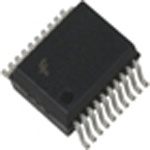
ICGOO电子元器件商城为您提供74ACT245SJ由Fairchild Semiconductor设计生产,在icgoo商城现货销售,并且可以通过原厂、代理商等渠道进行代购。 74ACT245SJ价格参考。Fairchild Semiconductor74ACT245SJ封装/规格:逻辑 - 缓冲器,驱动器,接收器,收发器, Transceiver, Non-Inverting 1 Element 8 Bit per Element 3-State Output 20-SOP。您可以下载74ACT245SJ参考资料、Datasheet数据手册功能说明书,资料中有74ACT245SJ 详细功能的应用电路图电压和使用方法及教程。
ON Semiconductor的74ACT245SJ是一款高速CMOS八位双向收发器,属于逻辑缓冲器/驱动器/接收器/收发器类别。该器件基于TTL兼容的ACT系列技术,具有高驱动能力与低功耗特性,广泛应用于需要双向数据传输的数字系统中。

典型应用场景包括:
1. 总线驱动与隔离:在微处理器、微控制器或FPGA系统中,用于驱动数据总线,实现不同模块之间的电气隔离与信号增强,提升系统稳定性。
2. 双向数据通信:适用于需要在两个方向上传输数据的场合,如CPU与外设之间的数据交换、存储器接口扩展等。
3. 工业控制设备:在PLC、工控机等设备中作为电平转换和信号缓冲器件,确保信号完整性。
4. 通信系统:用于板间或模块间的数据传输接口,支持高速、可靠的数字信号传递。
5. 测试与测量仪器:在数字电路测试设备中作为信号调理单元,提高驱动能力和抗干扰性能。

74ACT245SJ工作电压为5V,具备三态输出功能,可通过方向控制(DIR)和输出使能(OE)引脚灵活控制数据流向,适合构建紧凑高效的数字接口电路。其SOP封装形式便于PCB布局,适用于对空间和功耗有要求的中等密度设计场景。
| 参数 | 数值 |
| 产品目录 | 集成电路 (IC)半导体 |
| 描述 | IC TRANSCVR TRI-ST 8BIT 20SOP总线收发器 Octal Bidir Trans |
| 产品分类 | |
| 品牌 | Fairchild Semiconductor |
| 产品手册 | |
| 产品图片 |
|
| rohs | 符合RoHS无铅 / 符合限制有害物质指令(RoHS)规范要求 |
| 产品系列 | 逻辑集成电路,总线收发器,Fairchild Semiconductor 74ACT245SJ74ACT |
| 数据手册 | |
| 产品型号 | 74ACT245SJ |
| 产品种类 | 总线收发器 |
| 传播延迟时间 | 8 ns |
| 低电平输出电流 | 24 mA |
| 供应商器件封装 | 20-SOIC |
| 元件数 | 1 |
| 功能 | Transceiver |
| 包装 | 管件 |
| 单位重量 | 481.500 mg |
| 商标 | Fairchild Semiconductor |
| 安装类型 | 表面贴装 |
| 安装风格 | SMD/SMT |
| 封装 | Tube |
| 封装/外壳 | 20-SOIC(0.209",5.30mm 宽) |
| 封装/箱体 | SOP-20 |
| 工作温度 | -40°C ~ 85°C |
| 工厂包装数量 | 38 |
| 最大工作温度 | + 85 C |
| 最小工作温度 | - 40 C |
| 极性 | Non-Inverting |
| 标准包装 | 38 |
| 每元件位数 | 8 |
| 每芯片的通道数量 | 8 |
| 电压-电源 | 4.5 V ~ 5.5 V |
| 电流-输出高,低 | 24mA,24mA |
| 电源电压-最大 | 5.5 V |
| 电源电压-最小 | 4.5 V |
| 电路数量 | 8 |
| 系列 | 74ACT245 |
| 输入电平 | TTL |
| 输出电平 | CMOS |
| 输出类型 | 3-State |
| 逻辑类型 | CMOS |
| 逻辑系列 | ACT |
| 高电平输出电流 | - 24 mA |


- 商务部:美国ITC正式对集成电路等产品启动337调查
- 曝三星4nm工艺存在良率问题 高通将骁龙8 Gen1或转产台积电
- 太阳诱电将投资9.5亿元在常州建新厂生产MLCC 预计2023年完工
- 英特尔发布欧洲新工厂建设计划 深化IDM 2.0 战略
- 台积电先进制程称霸业界 有大客户加持明年业绩稳了
- 达到5530亿美元!SIA预计今年全球半导体销售额将创下新高
- 英特尔拟将自动驾驶子公司Mobileye上市 估值或超500亿美元
- 三星加码芯片和SET,合并消费电子和移动部门,撤换高东真等 CEO
- 三星电子宣布重大人事变动 还合并消费电子和移动部门
- 海关总署:前11个月进口集成电路产品价值2.52万亿元 增长14.8%


PDF Datasheet 数据手册内容提取
Is Now Part of To learn more about ON Semiconductor, please visit our website at www.onsemi.com Please note: As part of the Fairchild Semiconductor integration, some of the Fairchild orderable part numbers will need to change in order to meet ON Semiconductor’s system requirements. Since the ON Semiconductor product management systems do not have the ability to manage part nomenclature that utilizes an underscore (_), the underscore (_) in the Fairchild part numbers will be changed to a dash (-). This document may contain device numbers with an underscore (_). Please check the ON Semiconductor website to verify the updated device numbers. The most current and up-to-date ordering information can be found at www.onsemi.com. Please email any questions regarding the system integration to Fairchild_questions@onsemi.com. ON Semiconductor and the ON Semiconductor logo are trademarks of Semiconductor Components Industries, LLC dba ON Semiconductor or its subsidiaries in the United States and/or other countries. ON Semiconductor owns the rights to a number of patents, trademarks, copyrights, trade secrets, and other intellectual property. A listing of ON Semiconductor’s product/patent coverage may be accessed at www.onsemi.com/site/pdf/Patent-Marking.pdf. ON Semiconductor reserves the right to make changes without further notice to any products herein. ON Semiconductor makes no warranty, representation or guarantee regarding the suitability of its products for any particular purpose, nor does ON Semiconductor assume any liability arising out of the application or use of any product or circuit, and specifically disclaims any and all liability, including without limitation special, consequential or incidental damages. Buyer is responsible for its products and applications using ON Semiconductor products, including compliance with all laws, regulations and safety requirements or standards, regardless of any support or applications information provided by ON Semiconductor. “Typical” parameters which may be provided in ON Semiconductor data sheets and/or specifications can and do vary in different applications and actual performance may vary over time. All operating parameters, including “Typicals” must be validated for each customer application by customer’s technical experts. ON Semiconductor does not convey any license under its patent rights nor the rights of others. ON Semiconductor products are not designed, intended, or authorized for use as a critical component in life support systems or any FDA Class 3 medical devices or medical devices with a same or similar classification in a foreign jurisdiction or any devices intended for implantation in the human body. Should Buyer purchase or use ON Semiconductor products for any such unintended or unauthorized application, Buyer shall indemnify and hold ON Semiconductor and its officers, employees, subsidiaries, affiliates, and distributors harmless against all claims, costs, damages, and expenses, and reasonable attorney fees arising out of, directly or indirectly, any claim of personal injury or death associated with such unintended or unauthorized use, even if such claim alleges that ON Semiconductor was negligent regarding the design or manufacture of the part. ON Semiconductor is an Equal Opportunity/Affirmative Action Employer. This literature is subject to all applicable copyright laws and is not for resale in any manner.
7 4 A C January 2008 2 4 5 , 7 4 A 74AC245, 74ACT245 C T Octal Bidirectional Transceiver with 3-STATE 2 4 5 Inputs/Outputs — O c Features General Description t a l ■ ICC and IOZ reduced by 50% The AC/ACT245 contains eight non-inverting bidirec- B ■ Non-inverting buffers tional buffers with 3-STATE outputs and is intended for id ■ Bidirectional data path bus-oriented applications. Current sinking capability is ir e 24mA at both the A and B ports. The Transmit/Receive ■ A and B outputs source/sink 24mA c (T/R) input determines the direction of data flow through ti ■ ACT245 has TTL-compatible inputs the bidirectional transceiver. Transmit (active-HIGH) on enables data from A ports to B ports; Receive (active- a l LOW) enables data from B ports to A ports. The Output T r Enable input, when HIGH, disables both A and B ports a n by placing them in a HIGH Z condition. s c e i v e r w Ordering Information it h Package 3 - S Order Number Number Package Description T A 74AC245SC M20B 20-Lead Small Outline Integrated Circuit (SOIC), JEDEC MS-013, 0.300" Wide T E 74AC245SJ M20D 20-Lead Small Outline Package (SOP), EIAJ TYPE II, 5.3mm Wide I n 74AC245MTC MTC20 20-Lead Thin Shrink Small Outline Package (TSSOP), JEDEC MO-153, p 4.4mm Wide u t s 74AC245PC N20A 20-Lead Plastic Dual-In-Line Package (PDIP), JEDEC MS-001, 0.300" Wide / O 74ACT245SC M20B 20-Lead Small Outline Integrated Circuit (SOIC), JEDEC MS-013, 0.300" Wide u t p 74ACT245SJ M20D 20-Lead Small Outline Package (SOP), EIAJ TYPE II, 5.3mm Wide u t 74ACT245MSA MSA20 20-Lead Shrink Small Outline Package (SSOP), JEDEC MO-150, 5.3mm Wide s 74ACT245MTC MTC20 20-Lead Thin Shrink Small Outline Package (TSSOP), JEDEC MO-153, 4.4mm Wide 74ACT245PC N20A 20-Lead Plastic Dual-In-Line Package (PDIP), JEDEC MS-001, 0.300" Wide Device also available in Tape and Reel. Specify by appending suffix letter “X” to the ordering number. All packages are lead free per JEDEC: J-STD-020B standard. ©1988 Fairchild Semiconductor Corporation www.fairchildsemi.com 74AC245, 74ACT245 Rev. 1.5.0
7 4 Connection Diagram Logic Symbol A C 2 4 5 , 7 4 A C T 2 4 5 — O IEEE/IEC c t a l B i d i r e c t i o Pin Description n a l T Pin r a Names Description n s OE Output Enable Input c e T/R Transmit/Receive Input iv e A –A Side A 3-STATE Inputs or 3-STATE r 0 7 Outputs w i t B –B Side B 3-STATE Inputs or 3-STATE h 0 7 Outputs 3 - S T A T Truth Table E I Inputs n p u OE T/R Outputs t s L L Bus B Data to Bus A /O u L H Bus A Data to Bus B t p H X HIGH-Z State u t s H = HIGH Voltage Level L = LOW Voltage Level X = Immaterial ©1988 Fairchild Semiconductor Corporation www.fairchildsemi.com 74AC245, 74ACT245 Rev. 1.5.0 2
7 4 Absolute Maximum Ratings A C Stresses exceeding the absolute maximum ratings may damage the device. The device may not function or be 2 4 operable above the recommended operating conditions and stressing the parts to these levels is not recommended. 5 In addition, extended exposure to stresses above the recommended operating conditions may affect device reliability. , 7 The absolute maximum ratings are stress ratings only. 4 A Symbol Parameter Rating C T V Supply Voltage −0.5V to +7.0V 2 CC 4 5 IIK DC Input Diode Current — V = −0.5V −20mA I O VI = VCC + 0.5 +20mA c t V DC Input Voltage −0.5V to V + 0.5V a I CC l B I DC Output Diode Current OK i d V = −0.5V −20mA i O r e V = V + 0.5V +20mA c O CC t V DC Output Voltage −0.5V to V + 0.5V io O CC n I DC Output Source or Sink Current ±50mA a O l ICC or IGND DC VCC or Ground Current per Output Pin ±50mA Tr a T Storage Temperature −65°C to +150°C n STG s T Junction Temperature 140°C c J e i v e r Recommended Operating Conditions w i t The Recommended Operating Conditions table defines the conditions for actual device operation. Recommended h operating conditions are specified to ensure optimal performance to the datasheet specifications. Fairchild does not 3 - recommend exceeding them or designing to absolute maximum ratings. S T A Symbol Parameter Rating T E VCC Supply Voltage I n AC 2.0V to 6.0V p u ACT 4.5V to 5.5V t s VI Input Voltage 0V to VCC /O u V Output Voltage 0V to V O CC t p T Operating Temperature −40°C to +85°C u A t ∆V / ∆t Minimum Input Edge Rate, AC Devices: 125mV/ns s V from 30% to 70% of V ,V @ 3.3V, 4.5V, 5.5V IN CC CC ∆V / ∆t Minimum Input Edge Rate, ACT Devices: 125mV/ns V from 0.8V to 2.0V, V @ 4.5V, 5.5V IN CC ©1988 Fairchild Semiconductor Corporation www.fairchildsemi.com 74AC245, 74ACT245 Rev. 1.5.0 3
7 4 DC Electrical Characteristics for AC A C 2 TA = +25°C TA = −40°C to +85°C 4 5 Symbol Parameter VCC (V) Conditions Typ. Guaranteed Limits Units , 7 VIH Minimum HIGH Level 3.0 VOUT = 0.1V or 1.5 2.1 2.1 V 4A Input Voltage V – 0.1V C 4.5 CC 2.25 3.15 3.15 T 2 5.5 2.75 3.85 3.85 4 5 VIL Maximum LOW Level 3.0 VOUT = 0.1V or 1.5 0.9 0.9 V — Input Voltage V – 0.1V 4.5 CC 2.25 1.35 1.35 O 5.5 2.75 1.65 1.65 c t a VOH Minimum HIGH Level 3.0 IOUT = –50µA 2.99 2.9 2.9 V l Output Voltage B 4.5 4.49 4.4 4.4 i d 5.5 5.49 5.4 5.4 ir e 3.0 V = V or V , 2.56 2.46 c IN IL IH t i I = –12mA o OH n 4.5 V = V or V , 3.86 3.76 a IN IL IH l T IOH = –24mA ra 5.5 V = V or V , 4.86 4.76 n IN IL IH s I = –24mA(1) c OH e V Maximum LOW Level 3.0 I = 50µA 0.002 0.1 0.1 V iv OL OUT e Output Voltage 4.5 0.001 0.1 0.1 r w 5.5 0.001 0.1 0.1 i t h 3.0 VIN = VIL or VIH, 0.36 0.44 3 I = 12mA -S OL T 4.5 V = V or V , 0.36 0.44 A IN IL IH T I = 24mA E OL 5.5 V = V or V , 0.36 0.44 In IN IL IH p I = 24mA(1) u OL t I (2) Maximum Input 5.5 V = V , GND ±0.1 ±1.0 µA s IN I CC /O Leakage Current u IOLD Minimum Dynamic 5.5 VOLD = 1.65V Max. 75 mA tp IOHD Output Current(3) 5.5 VOHD = 3.85V Min. −75 mA uts I (2) Maximum Quiescent 5.5 V = V or GND 4.0 40.0 µA CC IN CC Supply Current I Maximum I/O 5.5 V (OE) = V , V ; ±0.3 ±3.0 µA OZT I IL IH Leakage Current V = V , GND; I CC V = V , GND O CC Notes: 1. All outputs loaded; thresholds on input associated with output under test. 2. I and I @ 3.0V are guaranteed to be less than or equal to the respective limit @ 5.5V V . IN CC CC 3. Maximum test duration 2.0ms, one output loaded at a time. ©1988 Fairchild Semiconductor Corporation www.fairchildsemi.com 74AC245, 74ACT245 Rev. 1.5.0 4
7 4 DC Electrical Characteristics for ACT A C 2 TA = +25°C TA = −40°C to +85°C 4 5 Symbol Parameter VCC (V) Conditions Typ. Guaranteed Limits Units , 7 VIH Minimum HIGH Level 4.5 VOUT = 0.1V or 1.5 2.0 2.0 V 4A Input Voltage V − 0.1V C 5.5 CC 1.5 2.0 2.0 T VIL Maximum LOW 4.5 VOUT = 0.1V or 1.5 0.8 0.8 V 24 Level Input Voltage V − 0.1V 5 5.5 CC 1.5 0.8 0.8 — VOH Minimum HIGH Level 4.5 IOUT = −50µA 4.49 4.4 4.4 V O Output Voltage 5.5 5.49 5.4 5.4 c t a 4.5 VIN = VIL or VIH, 3.86 3.76 l B IOH = −24mA id 5.5 VIN = VIL or VIH, 4.86 4.76 ire I = −24mA(4) c OH t i V Maximum LOW 4.5 I = 50µA 0.001 0.1 0.1 V o OL OUT n Level Output Voltage 5.5 0.001 0.1 0.1 a l T 4.5 VIN = VIL or VIH, 0.36 0.44 ra I = 24mA n OL s 5.5 V = V or V , 0.36 0.44 c IN IL IH e I = 24mA(4) iv OL e I Maximum Input 5.5 V = V , GND ±0.1 ±1.0 µA r IN I CC w Leakage Current i t I Maximum I /Input 5.5 V = V − 2.1V 0.6 1.5 mA h CCT CC I CC 3 I Minimum Dynamic 5.5 V = 1.65V Max. 75 mA - OLD OLD S IOHD Output Current(5) 5.5 VOHD = 3.85V Min. −75 mA TA ICC Maximum Quiescent 5.5 VIN = VCC or GND 4.0 40.0 µA TE Supply Current I n I Maximum I/O 5.5 V (OE) = V , V ; ±0.3 ±3.0 µA p OZT I IL IH u Leakage Current VVOI = = V VCCCC, ,G GNNDD; ts/O Notes: u t 4. All outputs loaded; thresholds on input associated with output under test. p u 5. Maximum test duration 2.0ms, one output loaded at a time. ts ©1988 Fairchild Semiconductor Corporation www.fairchildsemi.com 74AC245, 74ACT245 Rev. 1.5.0 5
7 4 AC Electrical Characteristics for AC A C 2 TA = +25°C, TA = −40°C to +85°C, 4 CL = 50pF CL = 50pF 5, 7 Symbol Parameter V (V)(6) Min. Typ. Max. Min. Max. Units 4 CC A t Propagation Delay, 3.3 1.5 5.0 8.5 1.0 9.0 ns C PLH T A to B or B to A n n n n 5.0 1.5 3.5 6.5 1.0 7.0 2 4 t Propagation Delay, 3.3 1.5 5.0 8.5 1.0 9.0 ns 5 PHL — A to B or B to A n n n n 5.0 1.5 3.5 6.0 1.0 7.0 O tPZH Output Enable Time 3.3 2.5 7.0 11.5 2.0 12.5 ns c t 5.0 1.5 5.0 8.5 1.0 9.0 a l B t Output Enable Time 3.3 2.5 7.5 12.0 2.0 13.5 ns PZL i d 5.0 1.5 5.5 9.0 1.0 9.5 i r e t Output Disable Time 3.3 2.0 6.5 12.0 1.0 12.5 ns c PHZ t i 5.0 1.5 5.5 9.0 1.0 10.0 o n t Output Disable Time 3.3 2.0 7.0 11.5 1.5 13.0 ns a PLZ l T 5.0 1.5 5.5 9.0 1.0 10.0 r a n Note: s 6. Voltage range 3.3 is 3.3V ± 0.3V. Voltage range 5.0 is 5.0V ± 0.5V. c e i v e r AC Electrical Characteristics for ACT w i T = +25°C, T = −40°C to +85°C, th A A C = 50pF C = 50pF 3 L L - S Symbol Parameter V (V)(7) Min. Typ. Max. Min. Max. Units T CC A t Propagation Delay, 5.0 1.5 4.0 7.5 1.5 8.0 ns T PLH E An to Bn or Bn to An I n tPHL Propagation Delay, 5.0 1.5 4.0 8.0 1.0 9.0 ns p A to B or B to A u n n n n t s tPZH Output Enable Time 5.0 1.5 5.0 10.0 1.5 11.0 ns /O t Output Enable Time 5.0 1.5 5.5 10.0 1.5 12.0 ns u PZL t p tPHZ Output Disable Time 5.0 1.5 5.5 10.0 1.0 11.0 ns u t t Output Disable Time 5.0 2.0 5.0 10.0 1.5 11.0 ns s PLZ Note: 7. Voltage range 5.0 is 5.0V ± 0.5V. Capacitance Symbol Parameter Conditions Typ. Units C Input Capacitance V = OPEN 4.5 pF IN CC C Input/Output Capacitance V = 5.0V 15.0 pF I/O CC C Power Dissipation Capacitance V = 5.0V 45.0 pF PD CC ©1988 Fairchild Semiconductor Corporation www.fairchildsemi.com 74AC245, 74ACT245 Rev. 1.5.0 6
7 4 Physical Dimensions A C 2 4 13.00 5 12.60 , A 7 4 11.43 A C 20 11 T B 2 4 5 — 9.50 O 10.65 7.60 c t 10.00 7.40 a l B 2.25 i d i r e c t i 1 10 0.65 o PINONE 0.51 1.27 1.27 n INDICATOR 0.35 a l 0.25 M C B A T r LANDPATTERNRECOMMENDATION a n s c 2.65MAX SEEDETAILA e i v e 0.33 r C 0.20 w i t 0.30 0.10 C h 00..7255X45° 0.10 SEATINGPLANE 3-S NOTES:UNLESSOTHERWISESPECIFIED T A (R0.10) T A) THISPACKAGECONFORMSTOJEDEC E (R0.10) GAGEPLANE MS-013,VARIATIONAC,ISSUEE In B) ALLDIMENSIONSAREINMILLIMETERS. p 8° 0.25 u 0° C) DIMENSIONSDONOTINCLUDEMOLD t FLASHORBURRS. s / 1.27 D) CONFORMSTOASMEY14.5M-1994 O 0.40 SEATINGPLANE E) LANDPATTERNSTANDARD:SOIC127P1030X265-20L ut p (1.40) DETAILA F) DRAWINGFILENAME:MKT-M20BREV3 u SCALE:2:1 ts Figure 1. 20-Lead Small Outline Integrated Circuit (SOIC), JEDEC MS-013, 0.300" Wide Package drawings are provided as a service to customers considering Fairchild components. Drawings may change in any manner without notice. Please note the revision and/or date on the drawing and contact a Fairchild Semiconductor representative to verify or obtain the most recent revision. Package specifications do not expand the terms of Fairchild’s worldwide terms and conditions, specifically the warranty therein, which covers Fairchild products. Always visit Fairchild Semiconductor’s online packaging area for the most recent package drawings: http://www.fairchildsemi.com/packaging/ ©1988 Fairchild Semiconductor Corporation www.fairchildsemi.com 74AC245, 74ACT245 Rev. 1.5.0 7
7 4 Physical Dimensions (Continued) A C 2 4 5 , 7 4 A C T 2 4 5 — O c t a l B i d i r e c t i o n a l T r a n s c e i v e r w i t h 3 - S T A T E I n p u t s / O u t p u t s Figure 2. 20-Lead Small Outline Package (SOP), EIAJ TYPE II, 5.3mm Wide Package drawings are provided as a service to customers considering Fairchild components. Drawings may change in any manner without notice. Please note the revision and/or date on the drawing and contact a Fairchild Semiconductor representative to verify or obtain the most recent revision. Package specifications do not expand the terms of Fairchild’s worldwide terms and conditions, specifically the warranty therein, which covers Fairchild products. Always visit Fairchild Semiconductor’s online packaging area for the most recent package drawings: http://www.fairchildsemi.com/packaging/ ©1988 Fairchild Semiconductor Corporation www.fairchildsemi.com 74AC245, 74ACT245 Rev. 1.5.0 8
7 4 Physical Dimensions (Continued) A C 2 4 5 , 7 4 A C T 2 4 5 — O c t a l B i d i r e c t i o n a l T r a n s c e i v e r w i t h 3 - S T A T E I n p u t s / O u t p u t s Figure 3. 20-Lead Thin Shrink Small Outline Package (TSSOP), JEDEC MO-153, 4.4mm Wide Package drawings are provided as a service to customers considering Fairchild components. Drawings may change in any manner without notice. Please note the revision and/or date on the drawing and contact a Fairchild Semiconductor representative to verify or obtain the most recent revision. Package specifications do not expand the terms of Fairchild’s worldwide terms and conditions, specifically the warranty therein, which covers Fairchild products. Always visit Fairchild Semiconductor’s online packaging area for the most recent package drawings: http://www.fairchildsemi.com/packaging/ ©1988 Fairchild Semiconductor Corporation www.fairchildsemi.com 74AC245, 74ACT245 Rev. 1.5.0 9
7 4 Physical Dimensions (Continued) A C 2 4 26.92 5 , 7 24.89 4 A C T 2 4 PIN#1 7.11 5 — 6.09 O c t a l B i d i r 3.43 e c (0.97) 1.78 3.17 7.87 tio 7°TYP 5.33 MAX n 1.14 a l 7°TYP T r a n s c e i v e 2.54 3.55 r w 0.36 3.17 7.62 i t 0.38 MIN 10.92 MAX h 0.56 3 0.20 - S 0.35 T A .001[.025] C T E NOTES: In p u t s / O u t p u t s Figure 4. 20-Lead Plastic Dual-In-Line Package (PDIP), JEDEC MS-001, 0.300" Wide Package drawings are provided as a service to customers considering Fairchild components. Drawings may change in any manner without notice. Please note the revision and/or date on the drawing and contact a Fairchild Semiconductor representative to verify or obtain the most recent revision. Package specifications do not expand the terms of Fairchild’s worldwide terms and conditions, specifically the warranty therein, which covers Fairchild products. Always visit Fairchild Semiconductor’s online packaging area for the most recent package drawings: http://www.fairchildsemi.com/packaging/ ©1988 Fairchild Semiconductor Corporation www.fairchildsemi.com 74AC245, 74ACT245 Rev. 1.5.0 10
7 4 Physical Dimensions (Continued) A C 2 4 5 , 7 4 A C T 2 4 5 — O c t a l B i d i r e c t i o n a l T r a n s c e i v e r w i t h 3 - S T A T E I n p u t s / O u t p u t s Figure 5. 20-Lead Shrink Small Outline Package (SSOP), JEDEC MO-150, 5.3mm Wide Package drawings are provided as a service to customers considering Fairchild components. Drawings may change in any manner without notice. Please note the revision and/or date on the drawing and contact a Fairchild Semiconductor representative to verify or obtain the most recent revision. Package specifications do not expand the terms of Fairchild’s worldwide terms and conditions, specifically the warranty therein, which covers Fairchild products. Always visit Fairchild Semiconductor’s online packaging area for the most recent package drawings: http://www.fairchildsemi.com/packaging/ ©1988 Fairchild Semiconductor Corporation www.fairchildsemi.com 74AC245, 74ACT245 Rev. 1.5.0 11
7 4 A C 2 4 5 , 7 4 TRADEMARKS A Thefollowingincludesregisteredandunregisteredtrademarksandservicemarks,ownedbyFairchildSemiconductorand/oritsglobal C subsidiaries,andisnotintendedtobeanexhaustivelistofallsuchtrademarks. T 2 ACEx® FPS™ PDP-SPM™ SyncFET™ 45 BuilditNow™ FRFET® Power220® ® — CorePLUS™ GlobalPowerResourceSM Power247® ThePowerFranchise® CROSSVOLT™ GreenFPS™ POWEREDGE® O CTL™ GreenFPS™e-Series™ Power-SPM™ c CurrentTransferLogic™ GTO™ PowerTrench® TinyBoost™ ta EEZcoSSWPIATRCKH®™* iI-nLtoe™lliMAX™ PQrFoEgTra®mmableActiveDroop™ TTiinnyyBLougcikc™® l Bi ®™ IMMSeIOCgPRaLBOAuCNcOkA™URP™LER™ QQQTuSi™eOtpStoeerileesc™tronics™ TTTiiInnNyyYPPOoWPwMTeOr™™™ direc Fairchild® MicroFET™ RapidConfigure™ TinyWire™ tio FairchildSemiconductor® MicroPak™ SMARTSTART™ µSerDes™ n FACTQuietSeries™ MillerDrive™ SPM® UHC® a FACT® Motion-SPM™ STEALTH™ UltraFRFET™ l T FAST® OPTOLOGIC® SuperFET™ UniFET™ ra FastvCore™ OPTOPLANAR® SuperSOT™-3 VCX™ n FlashWriter®* ® SuperSOT™-6 s SuperSOT™-8 ce *EZSWITCH™andFlashWriter®aretrademarksofSystemGeneralCorporation,usedunderlicensebyFairchildSemiconductor. iv e r DISCLAIMER w i FAIRCHILDSEMICONDUCTORRESERVESTHERIGHTTOMAKECHANGESWITHOUTFURTHERNOTICETOANYPRODUCTS t h HEREINTOIMPROVERELIABILITY,FUNCTION,ORDESIGN.FAIRCHILDDOESNOTASSUMEANYLIABILITYARISINGOUTOFTHE 3 APPLICATIONORUSEOFANYPRODUCTORCIRCUITDESCRIBEDHEREIN;NEITHERDOESITCONVEYANYLICENSEUNDERITS - S PATENTRIGHTS,NORTHERIGHTSOFOTHERS.THESESPECIFICATIONSDONOTEXPANDTHETERMSOFFAIRCHILD’S T WORLDWIDETERMSANDCONDITIONS,SPECIFICALLYTHEWARRANTYTHEREIN,WHICHCOVERSTHESEPRODUCTS. A T E LIFESUPPORTPOLICY I n FAIRCHILD’SPRODUCTSARENOTAUTHORIZEDFORUSEASCRITICALCOMPONENTSINLIFESUPPORTDEVICESOR p SYSTEMSWITHOUTTHEEXPRESSWRITTENAPPROVALOFFAIRCHILDSEMICONDUCTORCORPORATION. u t s Asusedherein: / O 1. Life support devices or systems are devices or systems 2. A critical component in any component of a life support, u which, (a) are intended for surgical implant intothebodyor device, or system whose failure to perform can be t (b) support or sustain life, and (c) whose failure to perform reasonablyexpectedtocausethefailureofthelifesupport p u when properly used in accordance with instructions for use deviceorsystem,ortoaffectitssafetyoreffectiveness. t provided in the labeling, can be reasonably expected to s resultinasignificantinjuryoftheuser. PRODUCTSTATUSDEFINITIONS DefinitionofTerms DatasheetIdentification ProductStatus Definition Thisdatasheetcontainsthedesignspecificationsforproduct AdvanceInformation FormativeorInDesign development.Specificationsmaychangeinanymannerwithoutnotice. Thisdatasheetcontainspreliminarydata;supplementarydatawillbe Preliminary FirstProduction publishedatalaterdate.FairchildSemiconductorreservestherightto makechangesatanytimewithoutnoticetoimprovedesign. Thisdatasheetcontainsfinalspecifications.FairchildSemiconductor NoIdentificationNeeded FullProduction reservestherighttomakechangesatanytimewithoutnoticetoimprove thedesign. Thisdatasheetcontainsspecificationsonaproductthathasbeen Obsolete NotInProduction discontinuedbyFairchildSemiconductor.Thedatasheetisprintedfor referenceinformationonly. Rev.I32 ©1988 Fairchild Semiconductor Corporation www.fairchildsemi.com 74AC245, 74ACT245 Rev. 1.5.0 12
ON Semiconductor and are trademarks of Semiconductor Components Industries, LLC dba ON Semiconductor or its subsidiaries in the United States and/or other countries. ON Semiconductor owns the rights to a number of patents, trademarks, copyrights, trade secrets, and other intellectual property. A listing of ON Semiconductor’s product/patent coverage may be accessed at www.onsemi.com/site/pdf/Patent−Marking.pdf. ON Semiconductor reserves the right to make changes without further notice to any products herein. ON Semiconductor makes no warranty, representation or guarantee regarding the suitability of its products for any particular purpose, nor does ON Semiconductor assume any liability arising out of the application or use of any product or circuit, and specifically disclaims any and all liability, including without limitation special, consequential or incidental damages. Buyer is responsible for its products and applications using ON Semiconductor products, including compliance with all laws, regulations and safety requirements or standards, regardless of any support or applications information provided by ON Semiconductor. “Typical” parameters which may be provided in ON Semiconductor data sheets and/or specifications can and do vary in different applications and actual performance may vary over time. All operating parameters, including “Typicals” must be validated for each customer application by customer’s technical experts. ON Semiconductor does not convey any license under its patent rights nor the rights of others. ON Semiconductor products are not designed, intended, or authorized for use as a critical component in life support systems or any FDA Class 3 medical devices or medical devices with a same or similar classification in a foreign jurisdiction or any devices intended for implantation in the human body. Should Buyer purchase or use ON Semiconductor products for any such unintended or unauthorized application, Buyer shall indemnify and hold ON Semiconductor and its officers, employees, subsidiaries, affiliates, and distributors harmless against all claims, costs, damages, and expenses, and reasonable attorney fees arising out of, directly or indirectly, any claim of personal injury or death associated with such unintended or unauthorized use, even if such claim alleges that ON Semiconductor was negligent regarding the design or manufacture of the part. ON Semiconductor is an Equal Opportunity/Affirmative Action Employer. This literature is subject to all applicable copyright laws and is not for resale in any manner. PUBLICATION ORDERING INFORMATION LITERATURE FULFILLMENT: N. American Technical Support: 800−282−9855 Toll Free ON Semiconductor Website: www.onsemi.com Literature Distribution Center for ON Semiconductor USA/Canada 19521 E. 32nd Pkwy, Aurora, Colorado 80011 USA Europe, Middle East and Africa Technical Support: Order Literature: http://www.onsemi.com/orderlit Phone: 303−675−2175 or 800−344−3860 Toll Free USA/Canada Phone: 421 33 790 2910 Fax: 303−675−2176 or 800−344−3867 Toll Free USA/Canada Japan Customer Focus Center For additional information, please contact your local Email: orderlit@onsemi.com Phone: 81−3−5817−1050 Sales Representative © Semiconductor Components Industries, LLC www.onsemi.com www.onsemi.com 1