ICGOO在线商城 > 集成电路(IC) > 逻辑 - 缓冲器,驱动器,接收器,收发器 > SN74HC541DWR

 Datasheet下载
- 型号: SN74HC541DWR
- 制造商: Texas Instruments
- 库位|库存: xxxx|xxxx
- 要求:
| 数量阶梯 | 香港交货 | 国内含税 |
| +xxxx | $xxxx | ¥xxxx |
查看当月历史价格
查看今年历史价格
SN74HC541DWR产品简介:
ICGOO电子元器件商城为您提供SN74HC541DWR由Texas Instruments设计生产,在icgoo商城现货销售,并且可以通过原厂、代理商等渠道进行代购。 SN74HC541DWR价格参考¥1.58-¥2.10。Texas InstrumentsSN74HC541DWR封装/规格:逻辑 - 缓冲器,驱动器,接收器,收发器, Buffer, Non-Inverting 1 Element 8 Bit per Element 3-State Output 20-SOIC。您可以下载SN74HC541DWR参考资料、Datasheet数据手册功能说明书,资料中有SN74HC541DWR 详细功能的应用电路图电压和使用方法及教程。
SN74HC541DWR是德州仪器(Texas Instruments)生产的一款八路缓冲器/驱动器,属于高速CMOS逻辑系列。该器件包含8个非反相三态输出缓冲器,具有高驱动能力和低功耗特性,工作电压范围为2V至6V,兼容多种数字系统。

其主要应用场景包括:

1. 数字系统总线驱动:在微处理器、微控制器或FPGA系统中,用于增强数据或地址总线的驱动能力,实现信号远距离传输或驱动多个负载。

2. 存储器接口扩展:作为存储器与控制器之间的缓冲,提升信号完整性,减少负载对源端的影响。

3. 工业控制设备:广泛应用于PLC、I/O模块和工控机中,用于电平转换和信号隔离,提高系统抗干扰能力。

4. 通信系统:在多点通信或背板系统中,用作信号中继,确保数据稳定传输。

5. 消费类电子产品:如显示器模块、家电控制板等,用于驱动LED阵列或接口扩展。

SN74HC541DWR采用TSSOP封装,体积小,适合高密度PCB布局,并具备高噪声 immunity 和低静态功耗,适用于对稳定性与能效要求较高的场合。其三态输出功能支持多器件并联使用,便于构建复杂逻辑系统。
| 参数 | 数值 |
| 产品目录 | 集成电路 (IC)半导体 |
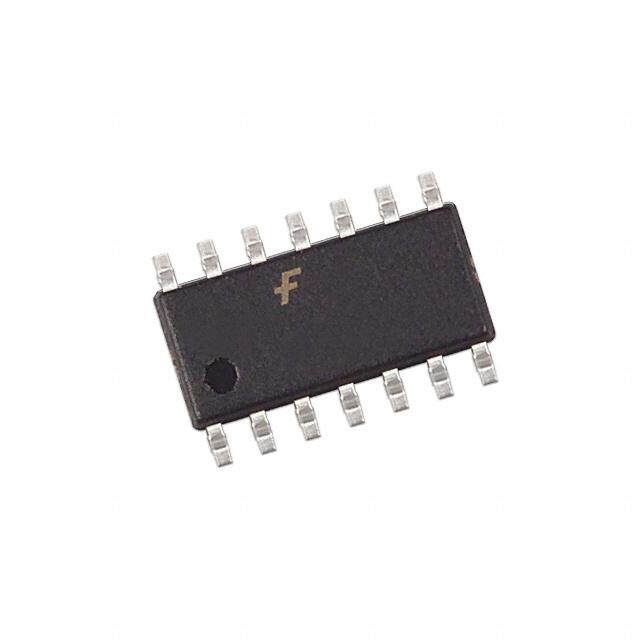
| 描述 | IC BUFF/DVR TRI-ST 8BIT 20SOIC缓冲器和线路驱动器 Tri-State Octal |
| 产品分类 | |
| 品牌 | Texas Instruments |
| 产品手册 | |
| 产品图片 |
|
| rohs | 符合RoHS无铅 / 符合限制有害物质指令(RoHS)规范要求 |
| 产品系列 | 逻辑集成电路,缓冲器和线路驱动器,Texas Instruments SN74HC541DWR74HC |
| 数据手册 | |
| 产品型号 | SN74HC541DWR |
| 产品目录页面 | |
| 产品种类 | 缓冲器和线路驱动器 |
| 传播延迟时间 | 165 ns at 2 V, 33 ns at 4.5 V, 28 ns at 6 V |
| 低电平输出电流 | 7.8 mA |
| 供应商器件封装 | 20-SOIC |
| 元件数 | 1 |
| 其它名称 | 296-1202-1 |
| 包装 | 剪切带 (CT) |
| 单位重量 | 500.700 mg |
| 商标 | Texas Instruments |
| 安装类型 | 表面贴装 |
| 安装风格 | SMD/SMT |
| 封装 | Reel |
| 封装/外壳 | 20-SOIC(0.295",7.50mm 宽) |
| 封装/箱体 | SOIC-20 |
| 工作温度 | -40°C ~ 85°C |
| 工厂包装数量 | 2000 |
| 最大工作温度 | + 85 C |
| 最小工作温度 | - 40 C |
| 极性 | Non-Inverting |
| 标准包装 | 1 |
| 每元件位数 | 8 |
| 每芯片的通道数量 | 8 |
| 电压-电源 | 2 V ~ 6 V |
| 电流-输出高,低 | 7.8mA,7.8mA |
| 电源电压-最大 | 6 V |
| 电源电压-最小 | 2 V |
| 电源电流 | 0.08 mA |
| 系列 | SN74HC541 |
| 输入线路数量 | 8 |
| 输出类型 | 3-State |
| 输出线路数量 | 8 |
| 逻辑类型 | 缓冲器/线路驱动器,非反相 |
| 逻辑系列 | HC |
| 高电平输出电流 | - 7.8 mA |


- 商务部:美国ITC正式对集成电路等产品启动337调查
- 曝三星4nm工艺存在良率问题 高通将骁龙8 Gen1或转产台积电
- 太阳诱电将投资9.5亿元在常州建新厂生产MLCC 预计2023年完工
- 英特尔发布欧洲新工厂建设计划 深化IDM 2.0 战略
- 台积电先进制程称霸业界 有大客户加持明年业绩稳了
- 达到5530亿美元!SIA预计今年全球半导体销售额将创下新高
- 英特尔拟将自动驾驶子公司Mobileye上市 估值或超500亿美元
- 三星加码芯片和SET,合并消费电子和移动部门,撤换高东真等 CEO
- 三星电子宣布重大人事变动 还合并消费电子和移动部门
- 海关总署:前11个月进口集成电路产品价值2.52万亿元 增长14.8%


PDF Datasheet 数据手册内容提取
Product Sample & Technical Tools & Support & Folder Buy Documents Software Community SN54HC541,SN74HC541 SCLS305D–JANUARY1996–REVISEDSEPTEMBER2016 SNx4HC541 Octal Buffers and Line Drivers With 3-State Outputs 1 Features 3 Description • WideOperatingVoltageRangeof2Vto6V These octal buffers and line drivers feature the 1 performance of the SNx4HC541 devices and a pinout • High-Current3-StateOutputsDriveBusLines with inputs and outputs on opposite sides of the DirectlyorUpto15LSTTLLoads package. This arrangement greatly facilitates printed • LowPowerConsumption,80-µAMaximumI circuitboardlayout. CC • Typicalt =10ns pd The 3-state outputs are controlled by a two-input • ±6-mAOutputDriveat5V NOR gate. If either output-enable (OE1 or OE2) input is high, all eight outputs are in the high-impedance • LowInputCurrentof1 µAMaximum state. The SNx4HC541 devices provide true data at • DataFlow-ThroughPinout(AllInputsonOpposite theoutputs. SideFromOutputs) DeviceInformation(1) 2 Applications PARTNUMBER PACKAGE BODYSIZE(NOM) • LEDs SN74HC541DW SOIC(20) 12.80mm×7.50mm • Servers SN74HC541DB SSOP(20) 7.20mm×5.30mm • PCsandNotebooks SN74HC541N PDIP(20) 24.33mm×6.35mm • WearableHealthandWellnessDevices SN74HC541NS SO(20) 12.60mm×5.30mm • ElectronicPointsofSale SN74HC541PW TSSOP(20) 6.50mm×4.40mm SN54HC541J CDIP(20) 24.20mm×6.92mm SN54HC541FK LCCC(20) 8.89mm×8.89mm (1) For all available packages, see the orderable addendum at theendofthedatasheet. LogicDiagram(PositiveLogic) 1 OE1 19 OE2 2 18 A1 Y1 ToSevenOtherChannels Copyright © 2016,Texas Instruments Incorporated 1 An IMPORTANT NOTICE at the end of this data sheet addresses availability, warranty, changes, use in safety-critical applications, intellectualpropertymattersandotherimportantdisclaimers.PRODUCTIONDATA. On products compliant to MIL-PRF-38535, all parameters are testedunlessotherwisenoted.Onallotherproducts,production processingdoesnotnecessarilyincludetestingofallparameters.
SN54HC541,SN74HC541 SCLS305D–JANUARY1996–REVISEDSEPTEMBER2016 www.ti.com Table of Contents 1 Features.................................................................. 1 6.15 TypicalCharacteristics............................................8 2 Applications........................................................... 1 7 ParameterMeasurementInformation..................9 3 Description............................................................. 1 8 DetailedDescription............................................ 10 4 RevisionHistory..................................................... 2 8.1 Overview.................................................................10 5 PinConfigurationandFunctions......................... 3 8.2 FunctionalBlockDiagram.......................................10 8.3 FeatureDescription.................................................10 6 Specifications......................................................... 4 8.4 DeviceFunctionalModes........................................10 6.1 AbsoluteMaximumRatings......................................4 9 ApplicationandImplementation........................ 11 6.2 ESDRatings..............................................................4 6.3 RecommendedOperatingConditions.......................4 9.1 ApplicationInformation............................................11 6.4 ThermalInformation..................................................5 9.2 TypicalApplication..................................................11 6.5 ElectricalCharacteristics,T =25°C........................5 10 PowerSupplyRecommendations..................... 13 A 6.6 ElectricalCharacteristics,SN54HC541....................5 11 Layout................................................................... 13 6.7 ElectricalCharacteristics,SN74HC541....................6 11.1 LayoutGuidelines.................................................13 6.8 SwitchingCharacteristics,C =50pF,T =25°C....6 11.2 LayoutExample....................................................13 L A 6.9 SwitchingCharacteristics,C =50pF,SN54HC541 6 12 DeviceandDocumentationSupport................. 14 L 6.10 SwitchingCharacteristics,C =50pF, 12.1 RelatedLinks........................................................14 L SN74HC541...............................................................7 12.2 ReceivingNotificationofDocumentationUpdates14 6.11 SwitchingCharacteristics,CL=150pF,TA=25°C 7 12.3 CommunityResources..........................................14 6.12 SwitchingCharacteristics,CL=150pF, 12.4 Trademarks...........................................................14 SN54HC541...............................................................7 12.5 ElectrostaticDischargeCaution............................14 6.13 SwitchingCharacteristics,C =150pF, L 12.6 Glossary................................................................14 SN74HC541...............................................................8 13 Mechanical,Packaging,andOrderable 6.14 OperatingCharacteristics........................................8 Information........................................................... 14 4 Revision History NOTE:Pagenumbersforpreviousrevisionsmaydifferfrompagenumbersinthecurrentversion. ChangesfromRevisionC(August2003)toRevisionD Page • AddedApplicationssection,ThermalInformationtable,ESDRatingstable,FeatureDescriptionsection,Device FunctionalModes,ApplicationandImplementationsection,PowerSupplyRecommendationssection,Layout section,DeviceandDocumentationSupportsection,andMechanical,Packaging,andOrderableInformationsection......1 • DeletedOrderingInformationtable,seeMechanical,Packaging,andOrderableInformationattheendofthedatasheet..1 • ChangedR forDBpackagefrom70°C/W:to90.2°C/W.................................................................................................... 5 θJA • ChangedR forDWpackagefrom58°C/W:to77.5°C/W................................................................................................... 5 θJA • ChangedR forNpackagefrom69°C/W:to45.2°C/W....................................................................................................... 5 θJA • ChangedR forNSpackagefrom60°C/W:to72.8°C/W.................................................................................................... 5 θJA • ChangedR forPWpackagefrom83°C/W:to98.3°C/W................................................................................................... 5 θJA 2 SubmitDocumentationFeedback Copyright©1996–2016,TexasInstrumentsIncorporated ProductFolderLinks:SN54HC541 SN74HC541
SN54HC541,SN74HC541 www.ti.com SCLS305D–JANUARY1996–REVISEDSEPTEMBER2016 5 Pin Configuration and Functions DB,DW,N,NS,J,orPWPackage 20-PinSSOP,SOIC,PDIP,SO,CDIP,orTSSOP FKPackage TopView 20-PinLCCC TopView A2 A1 OE1 VCC OE2 OE1 1 20 VCC A1 2 19 OE2 3 2 1 0 9 2 1 A2 3 18 Y1 A3 4 18 Y1 A3 4 17 Y2 A4 5 17 Y2 A4 5 16 Y3 A5 6 16 Y3 A5 6 15 Y4 A6 7 15 Y4 A6 7 14 Y5 A7 8 14 Y5 A7 8 13 Y6 0 1 2 3 A8 9 12 Y7 9 1 1 1 1 GND 10 11 Y8 Not to scale 8 D 8 7 6 A N Y Y Y G Not to scale PinFunctions PIN I/O DESCRIPTION NO. NAME 1 OE1 I Outputenable(activelow)BothOEmustbelowtoenableoutputs 2 A1 I Channel1input 3 A2 I Channel2input 4 A3 I Channel3input 5 A4 I Channel4input 6 A5 I Channel5input 7 A6 I Channel6input 8 A7 I Channel7input 9 A8 I Channel8input 10 GND — Ground 11 Y8 O Channel8output 12 Y7 O Channel7output 13 Y6 O Channel6output 14 Y5 O Channel5output 15 Y4 O Channel4output 16 Y3 O Channel3output 17 Y2 O Channel2output 18 Y1 O Channel1output 19 OE2 I Outputenable(activelow)bothOEmustbelowtoenableoutputs 20 V — Powerpin CC Copyright©1996–2016,TexasInstrumentsIncorporated SubmitDocumentationFeedback 3 ProductFolderLinks:SN54HC541 SN74HC541
SN54HC541,SN74HC541 SCLS305D–JANUARY1996–REVISEDSEPTEMBER2016 www.ti.com 6 Specifications 6.1 Absolute Maximum Ratings overoperatingfree-airtemperaturerange(unlessotherwisenoted)(1) MIN MAX UNIT V Supplyvoltage –0.5 7 V CC I Inputclampcurrent(2) V <0orV >V ±20 mA IK I I CC I Outputclampcurrent(2) V <0orV >V ±20 mA OK O O CC I Continuousoutputcurrent V =0toV ±35 mA O O CC ContinuouscurrentthroughV orGND ±70 mA CC T Storagetemperature –65 150 °C stg (1) StressesbeyondthoselistedunderAbsoluteMaximumRatingsmaycausepermanentdamagetothedevice.Thesearestressratings only,whichdonotimplyfunctionaloperationofthedeviceattheseoranyotherconditionsbeyondthoseindicatedunderRecommended OperatingConditions.Exposuretoabsolute-maximum-ratedconditionsforextendedperiodsmayaffectdevicereliability. (2) Theinputandoutputvoltageratingsmaybeexceedediftheinputandoutputcurrentratingsareobserved. 6.2 ESD Ratings VALUE UNIT Electrostatic Human-bodymodel(HBM),perANSI/ESDA/JEDECJS-001(1) ±2000 V V (ESD) discharge Charged-devicemodel(CDM),perJEDECspecificationJESD22-C101(2) ±1000 (1) JEDECdocumentJEP155statesthat500-VHBMallowssafemanufacturingwithastandardESDcontrolprocess. (2) JEDECdocumentJEP157statesthat250-VCDMallowssafemanufacturingwithastandardESDcontrolprocess. 6.3 Recommended Operating Conditions Seenote(1) MIN NOM MAX UNIT V Supplyvoltage 2 5 6 V CC V =2V 1.5 CC V High-levelinputvoltage V =4.5V 3.15 V IH CC V =6V 4.2 CC V =2V 0.5 CC V Low-levelinputvoltage V =4.5V 1.35 V IL CC V =6V 1.8 CC V Inputvoltage 0 V V I CC V Outputvoltage 0 V V O CC V =2V 1000 CC Δt/Δv Inputtransitionriseandfalltime V =4.5V 500 ns CC V =6V 400 CC SN54HC541 –55 125 T Operatingfree-airtemperature °C A SN74HC541 –40 85 (1) AllunusedinputsofthedevicemustbeheldatV orGNDtoensureproperdeviceoperation.SeeImplicationsofSloworFloating CC CMOSInputs,SCBA004. 4 SubmitDocumentationFeedback Copyright©1996–2016,TexasInstrumentsIncorporated ProductFolderLinks:SN54HC541 SN74HC541
SN54HC541,SN74HC541 www.ti.com SCLS305D–JANUARY1996–REVISEDSEPTEMBER2016 6.4 Thermal Information SN74HC541 THERMALMETRIC(1) DB DW N NS PW UNIT (SSOP) (SOIC) (PDIP) (SO) (TSSOP) 20PINS 20PINS 20PINS 20PINS 20PINS R Junction-to-ambientthermalresistance(2) 90.2 77.5 45.2 72.8 98.3 °C/W θJA R Junction-to-case(top)thermalresistance 51.7 42.9 31.3 39.1 33.5 °C/W θJC(top) R Junction-to-boardthermalresistance 45.3 45.4 26.1 40.3 49.2 °C/W θJB ψ Junction-to-topcharacterizationparameter 17.7 16.9 16.8 15.9 2.1 °C/W JT ψ Junction-to-boardcharacterizationparameter 44.9 44.9 26.0 39.9 48.7 °C/W JB (1) Formoreinformationabouttraditionalandnewthermalmetrics,seetheSemiconductorandICPackageThermalMetricsapplication report. (2) ThepackagethermalimpedanceiscalculatedinaccordancewithJESD51-7. 6.5 Electrical Characteristics, T = 25°C A overoperatingfree-airtemperaturerange(unlessotherwisenoted) PARAMETER TESTCONDITIONS V MIN TYP MAX UNIT CC 2V 1.9 1.998 I =–20µA 4.5V 4.4 4.499 OH V V =V orV 6V 5.9 5.999 V OH I IH IL I =–6mA 4.5V 3.98 4.3 OH I =–7.8mA 6V 5.48 5.8 OH 2V 0.002 0.1 I =20µA 4.5V 0.001 0.1 OL V V =V orV 6V 0.001 0.1 V OL I IH IL I =6mA 4.5V 0.17 0.26 OL I =7.8mA 6V 0.15 0.26 OL I V =V or0 6V ±0.1 ±100 nA I I CC I V =V or0 6V ±0.01 ±0.5 µA OZ O CC I V =V or0,I =0 6V 8 µA CC I CC O C 2Vto6V 3 10 pF i 6.6 Electrical Characteristics, SN54HC541 overoperatingfree-airtemperaturerange(unlessotherwisenoted) PARAMETER TESTCONDITIONS V MIN TYP MAX UNIT CC 2V 1.9 I =–20µA 4.5V 4.4 OH V V =V orV 6V 5.9 V OH I IH IL I =–6mA 4.5V 3.7 OH I =–7.8mA 6V 5.2 OH 2V 0.1 I =20µA 4.5V 0.1 OL V V =V orV 6V 0.1 V OL I IH IL I =6mA 4.5V 0.4 OL I =7.8mA 6V 0.4 OL I V =V or0 6V ±1000 nA I I CC I V =V or0 6V ±10 µA OZ O CC I V =V or0,I =0 6V 160 µA CC I CC O C 2Vto6V 10 pF i Copyright©1996–2016,TexasInstrumentsIncorporated SubmitDocumentationFeedback 5 ProductFolderLinks:SN54HC541 SN74HC541
SN54HC541,SN74HC541 SCLS305D–JANUARY1996–REVISEDSEPTEMBER2016 www.ti.com 6.7 Electrical Characteristics, SN74HC541 overoperatingfree-airtemperaturerange(unlessotherwisenoted) PARAMETER TESTCONDITIONS V MIN TYP MAX UNIT CC 2V 1.9 I =–20µA 4.5V 4.4 OH V V =V orV 6V 5.9 V OH I IH IL I =–6mA 4.5V 3.84 OH I =–7.8mA 6V 5.34 OH 2V 0.1 I =20µA 4.5V 0.1 OL V V =V orV 6V 0.1 V OL I IH IL I =6mA 4.5V 0.33 OL I =7.8mA 6V 0.33 OL I V =V or0 6V ±1000 nA I I CC I V =V or0 6V ±5 µA OZ O CC I V =V or0,I =0 6V 80 µA CC I CC O C 2Vto6V 10 pF i 6.8 Switching Characteristics, C = 50 pF, T = 25°C L A overrecommendedoperatingfree-airtemperaturerange,C =50pF(unlessotherwisenoted)(seeFigure3) L FROM TO PARAMETER V MIN TYP MAX UNIT (INPUT) (OUTPUT) CC 2V 40 115 t A Y 4.5V 12 23 ns pd 6V 10 20 2V 80 150 t OE Y 4.5V 17 30 ns en 6V 15 26 2V 40 150 t OE Y 4.5V 18 30 ns dis 6V 17 26 2V 28 60 t Y 4.5V 8 12 ns t 6V 6 10 6.9 Switching Characteristics, C = 50 pF, SN54HC541 L overrecommendedoperatingfree-airtemperaturerange,C =50pF(unlessotherwisenoted)(seeFigure3) L FROM TO PARAMETER V MIN TYP MAX UNIT (INPUT) (OUTPUT) CC 2V 171 t A Y 4.5V 34 ns pd 6V 29 2V 224 t OE Y 4.5V 45 ns en 6V 38 2V 224 t OE Y 4.5V 45 ns dis 6V 38 6 SubmitDocumentationFeedback Copyright©1996–2016,TexasInstrumentsIncorporated ProductFolderLinks:SN54HC541 SN74HC541
SN54HC541,SN74HC541 www.ti.com SCLS305D–JANUARY1996–REVISEDSEPTEMBER2016 Switching Characteristics, C = 50 pF, SN54HC541 (continued) L overrecommendedoperatingfree-airtemperaturerange,C =50pF(unlessotherwisenoted)(seeFigure3) L FROM TO PARAMETER V MIN TYP MAX UNIT (INPUT) (OUTPUT) CC 2V 90 t Y 4.5V 18 ns t 6V 15 6.10 Switching Characteristics, C = 50 pF, SN74HC541 L overrecommendedoperatingfree-airtemperaturerange,C =50pF(unlessotherwisenoted)(seeFigure3) L FROM TO PARAMETER V MIN TYP MAX UNIT (INPUT) (OUTPUT) CC 2V 144 t A Y 4.5V 29 ns pd 6V 25 2V 188 t OE Y 4.5V 38 ns en 6V 32 2V 188 t OE Y 4.5V 38 ns dis 6V 32 2V 75 t Y 4.5V 15 ns t 6V 13 6.11 Switching Characteristics, C = 150 pF, T = 25°C L A overrecommendedoperatingfree-airtemperaturerange,C =150pF(unlessotherwisenoted)(seeFigure3) L FROM TO PARAMETER V MIN TYP MAX UNIT (INPUT) (OUTPUT) CC 2V 65 165 t A Y 4.5V 16 33 ns pd 6V 14 28 2V 100 200 t OE Y 4.5V 20 40 ns en 6V 17 34 2V 45 210 t Y 4.5V 17 42 ns t 6V 13 36 6.12 Switching Characteristics, C = 150 pF, SN54HC541 L overrecommendedoperatingfree-airtemperaturerange,C =150pF(unlessotherwisenoted)(seeFigure3) L FROM TO PARAMETER V MIN TYP MAX UNIT (INPUT) (OUTPUT) CC 2V 246 t A Y 4.5V 49 ns pd 6V 42 2V 298 t OE Y 4.5V 60 ns en 6V 51 Copyright©1996–2016,TexasInstrumentsIncorporated SubmitDocumentationFeedback 7 ProductFolderLinks:SN54HC541 SN74HC541
SN54HC541,SN74HC541 SCLS305D–JANUARY1996–REVISEDSEPTEMBER2016 www.ti.com Switching Characteristics, C = 150 pF, SN54HC541 (continued) L overrecommendedoperatingfree-airtemperaturerange,C =150pF(unlessotherwisenoted)(seeFigure3) L FROM TO PARAMETER V MIN TYP MAX UNIT (INPUT) (OUTPUT) CC 2V 315 t Y 4.5V 63 ns t 6V 53 6.13 Switching Characteristics, C = 150 pF, SN74HC541 L overrecommendedoperatingfree-airtemperaturerange,C =150pF(unlessotherwisenoted)(seeFigure3) L FROM TO PARAMETER V MIN TYP MAX UNIT (INPUT) (OUTPUT) CC 2V 206 t A Y 4.5V 41 ns pd 6V 35 2V 250 t OE Y 4.5V 50 ns en 6V 43 2V 265 t Y 4.5V 53 ns t 6V 45 6.14 Operating Characteristics T =25°C A PARAMETER TESTCONDITIONS TYP UNIT C Powerdissipationcapacitanceperbuffer/driver Noload 35 pF pd 6.15 Typical Characteristics 80 100 tpd tpd 70 ten 90 ten tdis tt 60 tt 80 70 50 ns) ns) 60 e ( 40 e ( m m 50 Ti Ti 30 40 20 30 10 20 0 10 2 2.5 3 3.5 4 4.5 5 5.5 6 2 2.5 3 3.5 4 4.5 5 5.5 6 Vcc (Volts) Vcc (Volts) D001 D001 Figure1.TypicalDelayvs.V forC =50pF Figure2.TypicalDelayvs.V forC =150pF CC L CC L 8 SubmitDocumentationFeedback Copyright©1996–2016,TexasInstrumentsIncorporated ProductFolderLinks:SN54HC541 SN74HC541
SN54HC541,SN74HC541 www.ti.com SCLS305D–JANUARY1996–REVISEDSEPTEMBER2016 7 Parameter Measurement Information VCC PARAMETER RL CL S1 S2 S1 tPZH 50pF Open Closed Test ten 1kΩ or FromOutput Point RL tPZL 150pF Closed Open UnderTest tPHZ Open Closed CL S2 tdis tPLZ 1kΩ 50pF Closed Open (seeNoteA) 50pF tpdortt –– or Open Open 150pF LOADCIRCUIT VCC Input 50% 50% 0V tPLH tPHL In-Phase VOH 90% 90% Output 50% 50% 10% 10% VOL tr tf Output tPHL tPLH Control VCC VOH (Low-Level 50% 50% Out-of-Phase 90% 50% 50% 90% Enabling) 0V Output 10% 10% VOL tPZL tPLZ tf tr Output ≈VCC ≈VCC Waveform1 50% VOLTAGEWAVEFORMS PROPAGATIONDELAYANDOUTPUTTRANSITIONTIMES (SeeNoteB) 10% VOL tPZH tPHZ VCC Output VOH 90% 90% 90% Input 50% 50% Waveform2 50% 10% 10% 0V (SeeNoteB) ≈0V tr tf VOLTAGEWAVEFORM VOLTAGEWAVEFORMS INPUTRISEANDFALLTIMES ENABLEANDDISABLETIMESFOR3-STATEOUTPUTS A. C includesprobeandtest-fixturecapacitance. L B. Waveform1 is for an outputwith internalconditions such that theoutputis lowexceptwhendisabledby theoutput control. Waveform2isforanoutputwithinternalconditionssuchthattheoutputishighexceptwhendisabledbytheoutput control. C. Phase relationships between waveforms were chosen arbitrarily. All input pulses are supplied by generators having thefollowingcharacteristics:PRR≤1MHz,Z =50Ω,t =6ns,t =6ns. O r f D. Theoutputsaremeasuredoneatatimewithoneinputtransitionpermeasurement. E. t andt arethesameast . PLZ PHZ dis F. t andt arethesameast . PZL PZH en G. t andt arethesameast . PLH PHL pd Figure3. LoadCircuitandVoltageWaveforms Copyright©1996–2016,TexasInstrumentsIncorporated SubmitDocumentationFeedback 9 ProductFolderLinks:SN54HC541 SN74HC541
SN54HC541,SN74HC541 SCLS305D–JANUARY1996–REVISEDSEPTEMBER2016 www.ti.com 8 Detailed Description 8.1 Overview The SN74HC541 device has 8 inputs and outputs where data from the A inputs go to the Y outputs. The output enables of the device control whether the information from the A inputs go to the Y outputs. These enable pins cause the device to go into high Z if either OE1 or OE2 are high. The OEs should be tied to V through a pull CC up resistor to ensure the high impedance state during power up or power down; the minimum value of the resistorisdeterminedbythecurrentsinkingcapabilityofthedriver. 8.2 Functional Block Diagram 1 OE1 19 OE2 2 18 A1 Y1 ToSevenOtherChannels Copyright © 2016,Texas Instruments Incorporated Figure4. LogicDiagram(PositiveLogic) 8.3 Feature Description The SNx4HC541 has a wide operating voltage range of 2 V to 6 V. The device has multiple enable pins, and the devicepinoutenablessimpleboardlayoutwithoutputsacrossfrominputs. 8.4 Device Functional Modes Table1liststhefunctionalmodesoftheSNx4HC541. Table1.FunctionTable(EachBuffer/Driver) INPUTS OUTPUT OE1 OE2 A Y L L L L L L H H H X X Hi-Z X H X Hi-Z 10 SubmitDocumentationFeedback Copyright©1996–2016,TexasInstrumentsIncorporated ProductFolderLinks:SN54HC541 SN74HC541
SN54HC541,SN74HC541 www.ti.com SCLS305D–JANUARY1996–REVISEDSEPTEMBER2016 9 Application and Implementation NOTE Information in the following applications sections is not part of the TI component specification, and TI does not warrant its accuracy or completeness. TI’s customers are responsible for determining suitability of components for their purposes. Customers should validateandtesttheirdesignimplementationtoconfirmsystemfunctionality. 9.1 Application Information SN74HC541 is a wide range CMOS device that can be used over large voltage ranges. The device can be used anywhere from 2 to 6 Volts. The device can drive up to 6 mA of current at 5 Volts. This makes it perfect for driving bus lines directly or up to 15 LSTTL Loads. It can be used to drive anything from micro controllers and systemlogicdevicestoLEDs. 9.2 Typical Application OE1 VCC OE2 A1 Y1 Microcontroller System Logic LEDs Microcontroller or A8 Y8 System Logic GND Copyright © 2016,Texas Instruments Incorporated Figure5. TypicalApplicationDiagram 9.2.1 DesignRequirements This device uses CMOS technology and has a wide voltage range. Take care to avoid pulling too much current from the outputs as to not exceed 6 mA. Also, take care to not go over V voltage to avoid damage to the CC device. 9.2.2 DetailedDesignProcedure 1. RecommendedInputConditions – Risetimeandfalltimespecs:See(Δt/ΔV)intheRecommendedOperatingConditionstable. – Specifiedhighandlowlevels:See(VIHandVIL)intheRecommendedOperatingConditions table. – InputsshouldnotbepulledaboveV . CC 2. RecommendedOutputConditions – Loadcurrentsshouldnotexceed6mAforthepart – OutputsshouldnotbepulledaboveV . CC Copyright©1996–2016,TexasInstrumentsIncorporated SubmitDocumentationFeedback 11 ProductFolderLinks:SN54HC541 SN74HC541
SN54HC541,SN74HC541 SCLS305D–JANUARY1996–REVISEDSEPTEMBER2016 www.ti.com Typical Application (continued) 9.2.3 ApplicationCurve 1000 950 900 ns) 850 e ( 800 m Ti 750 n sitio 700 n 650 a Tr 600 ut p 550 n I 500 450 400 2 2.5 3 3.5 4 4.5 5 5.5 6 Vcc (Volts) D001 Figure6.InputTransitionTimevs.V CC 12 SubmitDocumentationFeedback Copyright©1996–2016,TexasInstrumentsIncorporated ProductFolderLinks:SN54HC541 SN74HC541
SN54HC541,SN74HC541 www.ti.com SCLS305D–JANUARY1996–REVISEDSEPTEMBER2016 10 Power Supply Recommendations The power supply can be any voltage between the MIN and MAX supply voltage rating located in the RecommendedOperatingConditionstable. Each V pin should have a good bypass capacitor to prevent power disturbance. For devices with a single CC supply, 0.1-μF is recommended; if there are multiple V pins, then 0.01-μF or 0.022-μF is recommended for CC each power pin. It is acceptable to parallel multiple bypass caps to reject different frequencies of noise. A 0.1-μF and a 1-μF are commonly used in parallel. The bypass capacitor should be installed as close to the power pin as possibleforbestresults. 11 Layout 11.1 Layout Guidelines Whenusingmultiplebitlogicdevicesinputsshouldneverfloat. In many cases, functions or parts of functions of digital logic devices are unused, for example, when only two inputs of a triple-input AND gate are used or only 3 of the 4 buffer gates are used. Such input pins should not be left unconnected because the undefined voltages at the outside connections result in undefined operational states. The Recommended Operating Conditions section specifies the rules that must be observed under all circumstances. All unused inputs of digital logic devices must be connected to a high or low bias to prevent them from floating. The logic level that should be applied to any particular unused input depends on the function of the device. Generally they will be tied to GND or V whichever makes more sense or is more convenient. It is CC generally acceptable to float outputs, unless the part is a transceiver. If the transceiver has an output enable pin, it disables the output section of the part when asserted. This does not disable the input section of the I/Os, so theycannotfloatwhendisabled. 11.2 Layout Example V cc Input Unused Input Output Unused Input Output Input Figure7. LayoutDiagram Copyright©1996–2016,TexasInstrumentsIncorporated SubmitDocumentationFeedback 13 ProductFolderLinks:SN54HC541 SN74HC541
SN54HC541,SN74HC541 SCLS305D–JANUARY1996–REVISEDSEPTEMBER2016 www.ti.com 12 Device and Documentation Support 12.1 Related Links The table below lists quick access links. Categories include technical documents, support and community resources,toolsandsoftware,andquickaccesstosampleorbuy. Table2.RelatedLinks TECHNICAL TOOLS& SUPPORT& PARTS PRODUCTFOLDER SAMPLE&BUY DOCUMENTS SOFTWARE COMMUNITY SN54HC541 Clickhere Clickhere Clickhere Clickhere Clickhere SN74HC541 Clickhere Clickhere Clickhere Clickhere Clickhere 12.2 Receiving Notification of Documentation Updates To receive notification of documentation updates, navigate to the device product folder on ti.com. In the upper right corner, click on Alert me to register and receive a weekly digest of any product information that has changed.Forchangedetails,reviewtherevisionhistoryincludedinanyreviseddocument. 12.3 Community Resources The following links connect to TI community resources. Linked contents are provided "AS IS" by the respective contributors. They do not constitute TI specifications and do not necessarily reflect TI's views; see TI's Terms of Use. TIE2E™OnlineCommunity TI'sEngineer-to-Engineer(E2E)Community.Createdtofostercollaboration amongengineers.Ate2e.ti.com,youcanaskquestions,shareknowledge,exploreideasandhelp solveproblemswithfellowengineers. DesignSupport TI'sDesignSupport QuicklyfindhelpfulE2Eforumsalongwithdesignsupporttoolsand contactinformationfortechnicalsupport. 12.4 Trademarks E2EisatrademarkofTexasInstruments. Allothertrademarksarethepropertyoftheirrespectiveowners. 12.5 Electrostatic Discharge Caution Thesedeviceshavelimitedbuilt-inESDprotection.Theleadsshouldbeshortedtogetherorthedeviceplacedinconductivefoam duringstorageorhandlingtopreventelectrostaticdamagetotheMOSgates. 12.6 Glossary SLYZ022—TIGlossary. Thisglossarylistsandexplainsterms,acronyms,anddefinitions. 13 Mechanical, Packaging, and Orderable Information The following pages include mechanical, packaging, and orderable information. This information is the most current data available for the designated devices. This data is subject to change without notice and revision of thisdocument.Forbrowser-basedversionsofthisdatasheet,refertotheleft-handnavigation. 14 SubmitDocumentationFeedback Copyright©1996–2016,TexasInstrumentsIncorporated ProductFolderLinks:SN54HC541 SN74HC541
PACKAGE OPTION ADDENDUM www.ti.com 24-Aug-2018 PACKAGING INFORMATION Orderable Device Status Package Type Package Pins Package Eco Plan Lead/Ball Finish MSL Peak Temp Op Temp (°C) Device Marking Samples (1) Drawing Qty (2) (6) (3) (4/5) JM38510/65711BRA ACTIVE CDIP J 20 1 TBD A42 N / A for Pkg Type -55 to 125 JM38510/ 65711BRA M38510/65711BRA ACTIVE CDIP J 20 1 TBD A42 N / A for Pkg Type -55 to 125 JM38510/ 65711BRA SN54HC541J ACTIVE CDIP J 20 1 TBD A42 N / A for Pkg Type -55 to 125 SN54HC541J SN74HC541DBR ACTIVE SSOP DB 20 2000 Green (RoHS CU NIPDAU Level-1-260C-UNLIM -40 to 85 HC541 & no Sb/Br) SN74HC541DW ACTIVE SOIC DW 20 25 Green (RoHS CU NIPDAU Level-1-260C-UNLIM -40 to 85 HC541 & no Sb/Br) SN74HC541DWE4 ACTIVE SOIC DW 20 25 Green (RoHS CU NIPDAU Level-1-260C-UNLIM -40 to 85 HC541 & no Sb/Br) SN74HC541DWG4 ACTIVE SOIC DW 20 25 Green (RoHS CU NIPDAU Level-1-260C-UNLIM -40 to 85 HC541 & no Sb/Br) SN74HC541DWR ACTIVE SOIC DW 20 2000 Green (RoHS CU NIPDAU Level-1-260C-UNLIM -40 to 85 HC541 & no Sb/Br) SN74HC541N ACTIVE PDIP N 20 20 Pb-Free CU NIPDAU N / A for Pkg Type -40 to 85 SN74HC541N (RoHS) SN74HC541NE4 ACTIVE PDIP N 20 20 Pb-Free CU NIPDAU N / A for Pkg Type -40 to 85 SN74HC541N (RoHS) SN74HC541NSR ACTIVE SO NS 20 2000 Green (RoHS CU NIPDAU Level-1-260C-UNLIM -40 to 85 HC541 & no Sb/Br) SN74HC541PW ACTIVE TSSOP PW 20 70 Green (RoHS CU NIPDAU Level-1-260C-UNLIM -40 to 85 HC541 & no Sb/Br) SN74HC541PWG4 ACTIVE TSSOP PW 20 70 Green (RoHS CU NIPDAU Level-1-260C-UNLIM -40 to 85 HC541 & no Sb/Br) SN74HC541PWR ACTIVE TSSOP PW 20 2000 Green (RoHS CU NIPDAU Level-1-260C-UNLIM -40 to 85 HC541 & no Sb/Br) SN74HC541PWT ACTIVE TSSOP PW 20 250 Green (RoHS CU NIPDAU Level-1-260C-UNLIM -40 to 85 HC541 & no Sb/Br) SNJ54HC541FK ACTIVE LCCC FK 20 1 TBD POST-PLATE N / A for Pkg Type -55 to 125 SNJ54HC 541FK SNJ54HC541J ACTIVE CDIP J 20 1 TBD A42 N / A for Pkg Type -55 to 125 SNJ54HC541J Addendum-Page 1
PACKAGE OPTION ADDENDUM www.ti.com 24-Aug-2018 (1) The marketing status values are defined as follows: ACTIVE: Product device recommended for new designs. LIFEBUY: TI has announced that the device will be discontinued, and a lifetime-buy period is in effect. NRND: Not recommended for new designs. Device is in production to support existing customers, but TI does not recommend using this part in a new design. PREVIEW: Device has been announced but is not in production. Samples may or may not be available. OBSOLETE: TI has discontinued the production of the device. (2) RoHS: TI defines "RoHS" to mean semiconductor products that are compliant with the current EU RoHS requirements for all 10 RoHS substances, including the requirement that RoHS substance do not exceed 0.1% by weight in homogeneous materials. Where designed to be soldered at high temperatures, "RoHS" products are suitable for use in specified lead-free processes. TI may reference these types of products as "Pb-Free". RoHS Exempt: TI defines "RoHS Exempt" to mean products that contain lead but are compliant with EU RoHS pursuant to a specific EU RoHS exemption. Green: TI defines "Green" to mean the content of Chlorine (Cl) and Bromine (Br) based flame retardants meet JS709B low halogen requirements of <=1000ppm threshold. Antimony trioxide based flame retardants must also meet the <=1000ppm threshold requirement. (3) MSL, Peak Temp. - The Moisture Sensitivity Level rating according to the JEDEC industry standard classifications, and peak solder temperature. (4) There may be additional marking, which relates to the logo, the lot trace code information, or the environmental category on the device. (5) Multiple Device Markings will be inside parentheses. Only one Device Marking contained in parentheses and separated by a "~" will appear on a device. If a line is indented then it is a continuation of the previous line and the two combined represent the entire Device Marking for that device. (6) Lead/Ball Finish - Orderable Devices may have multiple material finish options. Finish options are separated by a vertical ruled line. Lead/Ball Finish values may wrap to two lines if the finish value exceeds the maximum column width. Important Information and Disclaimer:The information provided on this page represents TI's knowledge and belief as of the date that it is provided. TI bases its knowledge and belief on information provided by third parties, and makes no representation or warranty as to the accuracy of such information. Efforts are underway to better integrate information from third parties. TI has taken and continues to take reasonable steps to provide representative and accurate information but may not have conducted destructive testing or chemical analysis on incoming materials and chemicals. TI and TI suppliers consider certain information to be proprietary, and thus CAS numbers and other limited information may not be available for release. In no event shall TI's liability arising out of such information exceed the total purchase price of the TI part(s) at issue in this document sold by TI to Customer on an annual basis. OTHER QUALIFIED VERSIONS OF SN54HC541, SN74HC541 : •Catalog: SN74HC541 •Military: SN54HC541 NOTE: Qualified Version Definitions: Addendum-Page 2
PACKAGE OPTION ADDENDUM www.ti.com 24-Aug-2018 •Catalog - TI's standard catalog product •Military - QML certified for Military and Defense Applications Addendum-Page 3
PACKAGE MATERIALS INFORMATION www.ti.com 12-Jul-2018 TAPE AND REEL INFORMATION *Alldimensionsarenominal Device Package Package Pins SPQ Reel Reel A0 B0 K0 P1 W Pin1 Type Drawing Diameter Width (mm) (mm) (mm) (mm) (mm) Quadrant (mm) W1(mm) SN74HC541DBR SSOP DB 20 2000 330.0 16.4 8.2 7.5 2.5 12.0 16.0 Q1 SN74HC541DWR SOIC DW 20 2000 330.0 24.4 10.8 13.3 2.7 12.0 24.0 Q1 SN74HC541NSR SO NS 20 2000 330.0 24.4 8.4 13.0 2.5 12.0 24.0 Q1 SN74HC541PWT TSSOP PW 20 250 330.0 16.4 6.95 7.1 1.6 8.0 16.0 Q1 PackMaterials-Page1
PACKAGE MATERIALS INFORMATION www.ti.com 12-Jul-2018 *Alldimensionsarenominal Device PackageType PackageDrawing Pins SPQ Length(mm) Width(mm) Height(mm) SN74HC541DBR SSOP DB 20 2000 367.0 367.0 38.0 SN74HC541DWR SOIC DW 20 2000 367.0 367.0 45.0 SN74HC541NSR SO NS 20 2000 367.0 367.0 45.0 SN74HC541PWT TSSOP PW 20 250 367.0 367.0 38.0 PackMaterials-Page2
None
None
None
None
None
PACKAGE OUTLINE DB0020A TSSOP - 2 mm max height SCALE 2.000 SMALL OUTLINE PACKAGE C 8.2 TYP 7.4 A 0.1 C PIN 1 INDEX AREA SEATING PLANE 18X 0.65 20 1 2X 7.5 5.85 6.9 NOTE 3 10 11 0.38 20X 0.22 5.6 B 0.1 C A B 5.0 NOTE 4 2 MAX (0.15) TYP 0.25 SEE DETAIL A GAGE PLANE 0 -8 0.95 0.05 MIN 0.55 DETA 15AIL A TYPICAL 4214851/A 12/2017 NOTES: 1. All linear dimensions are in millimeters. Any dimensions in parenthesis are for reference only. Dimensioning and tolerancing per ASME Y14.5M. 2. This drawing is subject to change without notice. 3. This dimension does not include mold flash, protrusions, or gate burrs. Mold flash, protrusions, or gate burrs shall not exceed 0.15 mm per side. 4. This dimension does not include interlead flash. Interlead flash shall not exceed 0.25 mm per side. 5. Reference JEDEC registration MO-150. www.ti.com
EXAMPLE BOARD LAYOUT DB0020A TSSOP - 2 mm max height SMALL OUTLINE PACKAGE 20X (1.85) SYMM (R0.05) TYP 1 20X (0.45) 20 SYMM 18X (0.65) 10 11 (7) LAND PATTERN EXAMPLE EXPOSED METAL SHOWN SCALE: 10X SOLDER MASK METAL METAL UNDER SOLDER MASK OPENING SOLDER MASK OPENING EXPOSED METAL EXPOSED METAL 0.07 MAX 0.07 MIN ALL AROUND ALL AROUND NON-SOLDER MASK SOLDER MASK DEFINED DEFINED (PREFERRED) SOLDE15.000 R MASK DETAILS 4214851/A 12/2017 NOTES: (continued) 6. Publication IPC-7351 may have alternate designs. 7. Solder mask tolerances between and around signal pads can vary based on board fabrication site. www.ti.com
EXAMPLE STENCIL DESIGN DB0020A TSSOP - 2 mm max height SMALL OUTLINE PACKAGE 20X (1.85) SYMM (R0.05) TYP 1 20X (0.45) 20 SYMM 18X (0.65) 10 11 (7) SOLDER PASTE EXAMPLE BASED ON 0.125 mm THICK STENCIL SCALE: 10X 4214851/A 12/2017 NOTES: (continued) 8. Laser cutting apertures with trapezoidal walls and rounded corners may offer better paste release. IPC-7525 may have alternate design recommendations. 9. Board assembly site may have different recommendations for stencil design. www.ti.com
None
PACKAGE OUTLINE DW0020A SOIC - 2.65 mm max height SCALE 1.200 SOIC C 10.63 SEATING PLANE TYP 9.97 A PIN 1 ID 0.1 C AREA 18X 1.27 20 1 13.0 2X 12.6 11.43 NOTE 3 10 11 0.51 20X 7.6 0.31 2.65 MAX B 7.4 0.25 C A B NOTE 4 0.33 TYP 0.10 0.25 SEE DETAIL A GAGE PLANE 0.3 1.27 0 - 8 0.1 0.40 DETAIL A TYPICAL 4220724/A 05/2016 NOTES: 1. All linear dimensions are in millimeters. Dimensions in parenthesis are for reference only. Dimensioning and tolerancing per ASME Y14.5M. 2. This drawing is subject to change without notice. 3. This dimension does not include mold flash, protrusions, or gate burrs. Mold flash, protrusions, or gate burrs shall not exceed 0.15 mm per side. 4. This dimension does not include interlead flash. Interlead flash shall not exceed 0.43 mm per side. 5. Reference JEDEC registration MS-013. www.ti.com
EXAMPLE BOARD LAYOUT DW0020A SOIC - 2.65 mm max height SOIC 20X (2) SYMM 1 20 20X (0.6) 18X (1.27) SYMM (R0.05) TYP 10 11 (9.3) LAND PATTERN EXAMPLE SCALE:6X SOOPLEDNEINRG MASK METAL MSOELTDAEL RU NMDAESRK SOOPLEDNEINRG MASK 0.07 MAX 0.07 MIN ALL AROUND ALL AROUND NON SOLDER MASK SOLDER MASK DEFINED DEFINED SOLDER MASK DETAILS 4220724/A 05/2016 NOTES: (continued) 6. Publication IPC-7351 may have alternate designs. 7. Solder mask tolerances between and around signal pads can vary based on board fabrication site. www.ti.com
EXAMPLE STENCIL DESIGN DW0020A SOIC - 2.65 mm max height SOIC 20X (2) SYMM 1 20 20X (0.6) 18X (1.27) SYMM 10 11 (9.3) SOLDER PASTE EXAMPLE BASED ON 0.125 mm THICK STENCIL SCALE:6X 4220724/A 05/2016 NOTES: (continued) 8. Laser cutting apertures with trapezoidal walls and rounded corners may offer better paste release. IPC-7525 may have alternate design recommendations. 9. Board assembly site may have different recommendations for stencil design. www.ti.com
IMPORTANTNOTICEANDDISCLAIMER TIPROVIDESTECHNICALANDRELIABILITYDATA(INCLUDINGDATASHEETS),DESIGNRESOURCES(INCLUDINGREFERENCE DESIGNS),APPLICATIONOROTHERDESIGNADVICE,WEBTOOLS,SAFETYINFORMATION,ANDOTHERRESOURCES“ASIS” ANDWITHALLFAULTS,ANDDISCLAIMSALLWARRANTIES,EXPRESSANDIMPLIED,INCLUDINGWITHOUTLIMITATIONANY IMPLIEDWARRANTIESOFMERCHANTABILITY,FITNESSFORAPARTICULARPURPOSEORNON-INFRINGEMENTOFTHIRD PARTYINTELLECTUALPROPERTYRIGHTS. TheseresourcesareintendedforskilleddevelopersdesigningwithTIproducts.Youaresolelyresponsiblefor(1)selectingtheappropriate TIproductsforyourapplication,(2)designing,validatingandtestingyourapplication,and(3)ensuringyourapplicationmeetsapplicable standards,andanyothersafety,security,orotherrequirements.Theseresourcesaresubjecttochangewithoutnotice.TIgrantsyou permissiontousetheseresourcesonlyfordevelopmentofanapplicationthatusestheTIproductsdescribedintheresource.Other reproductionanddisplayoftheseresourcesisprohibited.NolicenseisgrantedtoanyotherTIintellectualpropertyrightortoanythird partyintellectualpropertyright.TIdisclaimsresponsibilityfor,andyouwillfullyindemnifyTIanditsrepresentativesagainst,anyclaims, damages,costs,losses,andliabilitiesarisingoutofyouruseoftheseresources. TI’sproductsareprovidedsubjecttoTI’sTermsofSale(www.ti.com/legal/termsofsale.html)orotherapplicabletermsavailableeitheron ti.comorprovidedinconjunctionwithsuchTIproducts.TI’sprovisionoftheseresourcesdoesnotexpandorotherwisealterTI’sapplicable warrantiesorwarrantydisclaimersforTIproducts. MailingAddress:TexasInstruments,PostOfficeBox655303,Dallas,Texas75265 Copyright©2018,TexasInstrumentsIncorporated