ICGOO在线商城 > 集成电路(IC) > 逻辑 - 缓冲器,驱动器,接收器,收发器 > SN74LV245ATPWR
 Datasheet下载
- 型号: SN74LV245ATPWR
- 制造商: Texas Instruments
- 库位|库存: xxxx|xxxx
- 要求:
| 数量阶梯 | 香港交货 | 国内含税 |
| +xxxx | $xxxx | ¥xxxx |
查看当月历史价格
查看今年历史价格
SN74LV245ATPWR产品简介:
ICGOO电子元器件商城为您提供SN74LV245ATPWR由Texas Instruments设计生产,在icgoo商城现货销售,并且可以通过原厂、代理商等渠道进行代购。 SN74LV245ATPWR价格参考。Texas InstrumentsSN74LV245ATPWR封装/规格:逻辑 - 缓冲器,驱动器,接收器,收发器, Transceiver, Non-Inverting 1 Element 8 Bit per Element 3-State Output 20-TSSOP。您可以下载SN74LV245ATPWR参考资料、Datasheet数据手册功能说明书,资料中有SN74LV245ATPWR 详细功能的应用电路图电压和使用方法及教程。
SN74LV245ATPWR 是由 Texas Instruments(德州仪器)生产的一款逻辑器件,属于缓冲器、驱动器、接收器和收发器类别。其主要应用场景包括以下几个方面:

1. 总线数据传输:
   SN74LV245ATPWR 是一个 8 位双向总线收发器,支持三态输出功能。它常用于计算机系统、嵌入式设备和其他需要在不同总线之间传输数据的场景中。例如,在内存扩展或外设接口设计中,可以用来实现数据总线的隔离和驱动。

2. 信号电平转换:
   该芯片支持低电压操作(VCC = 2V 至 6.5V),能够处理不同的信号电平。因此,它可以用于连接具有不同电源电压的电路,比如将 3.3V 系统与 5V 系统进行通信。

3. 多路复用与解复用:
   在复杂的数字系统中,SN74LV245ATPWR 可以帮助管理多个数据流之间的切换,减少对外部控制逻辑的需求。通过方向控制引脚 (DIR) 和输出使能引脚 (OE),用户可以灵活地配置数据流向。

4. 工业自动化与控制:
   由于其高可靠性和广泛的电压范围,这款芯片也适用于工业环境中,例如 PLC(可编程逻辑控制器)、传感器接口以及数据采集系统等。

5. 消费电子与通信设备:
   在一些消费电子产品如打印机、扫描仪或网络设备中,SN74LV245ATPWR 能够提供必要的信号增强和保护功能,确保稳定的数据传输。

总之,SN74LV245ATPWR 的典型应用集中在需要高效、可靠的双向数据传输及电平转换的场合,广泛覆盖了从消费类电子产品到工业级解决方案的各种领域。
| 参数 | 数值 |
| 产品目录 | 集成电路 (IC)半导体 |
| 描述 | IC BUS TRANSCEIVER 8BIT 20TSSOP总线收发器 Octal Bus Trnscvr With 3-State Outputs |
| 产品分类 | |
| 品牌 | Texas Instruments |
| 产品手册 | http://www.ti.com/lit/gpn/sn74lv245at |
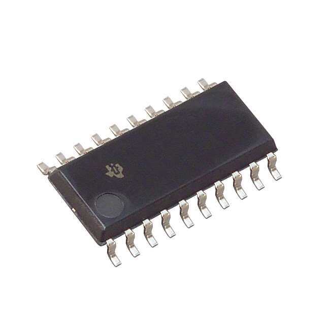
| 产品图片 |
|
| rohs | 符合RoHS无铅 / 符合限制有害物质指令(RoHS)规范要求 |
| 产品系列 | 逻辑集成电路,总线收发器,Texas Instruments SN74LV245ATPWR74LV |
| 数据手册 | |
| 产品型号 | SN74LV245ATPWR |
| 产品目录页面 | |
| 产品种类 | 总线收发器 |
| 传播延迟时间 | 7.7 ns |
| 低电平输出电流 | 16 mA |
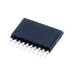
| 供应商器件封装 | 20-TSSOP |
| 元件数 | 1 |
| 其它名称 | 296-17771-1 |
| 功能 | Bus Transceiver |
| 包装 | 剪切带 (CT) |
| 单位重量 | 77 mg |
| 商标 | Texas Instruments |
| 安装类型 | 表面贴装 |
| 安装风格 | SMD/SMT |
| 封装 | Reel |
| 封装/外壳 | 20-TSSOP(0.173",4.40mm 宽) |
| 封装/箱体 | TSSOP-20 |
| 工作温度 | -40°C ~ 125°C |
| 工厂包装数量 | 2000 |
| 最大工作温度 | + 85 C |
| 最小工作温度 | - 40 C |
| 极性 | Non-Inverting |
| 标准包装 | 1 |
| 每元件位数 | 8 |
| 每芯片的通道数量 | 8 |
| 电压-电源 | 4.5 V ~ 5.5 V |
| 电流-输出高,低 | 16mA,16mA |
| 电源电压-最大 | 5.5 V |
| 电源电压-最小 | 4.5 V |
| 电路数量 | 8 |
| 系列 | SN74LV245AT |
| 输入电平 | TTL |
| 输出电平 | CMOS |
| 输出类型 | 3-State |
| 逻辑类型 | 收发器,非反相 |
| 逻辑系列 | LV-AT |
| 高电平输出电流 | - 16 mA |


- 商务部:美国ITC正式对集成电路等产品启动337调查
- 曝三星4nm工艺存在良率问题 高通将骁龙8 Gen1或转产台积电
- 太阳诱电将投资9.5亿元在常州建新厂生产MLCC 预计2023年完工
- 英特尔发布欧洲新工厂建设计划 深化IDM 2.0 战略
- 台积电先进制程称霸业界 有大客户加持明年业绩稳了
- 达到5530亿美元!SIA预计今年全球半导体销售额将创下新高
- 英特尔拟将自动驾驶子公司Mobileye上市 估值或超500亿美元
- 三星加码芯片和SET,合并消费电子和移动部门,撤换高东真等 CEO
- 三星电子宣布重大人事变动 还合并消费电子和移动部门
- 海关总署:前11个月进口集成电路产品价值2.52万亿元 增长14.8%


PDF Datasheet 数据手册内容提取
SN74LV245AT www.ti.com SCLS605D–DECEMBER2004–REVISEDJULY2013 OCTAL BUS TRANSCEIVER WITH 3-STATE OUTPUTS CheckforSamples:SN74LV245AT FEATURES DESCRIPTION 1 • InputsAreTTL-VoltageCompatible This octal bus transceiver is designed for asynchronous two-way communication between data • 4.5-Vto5.5-VV Operation CC buses. The control-function implementation minimizes • Typicaltpdof3.5nsat5V externaltimingrequirements. • TypicalV (OutputGroundBounce) <0.8V OLP The SN74LV245AT allows data transmission from the atVCC=5V,TA=25°C A bus to the B bus or from the B bus to the A bus, • TypicalV (OutputV Undershoot) >2.3V depending on the logic level at the direction-control OHV OH atV =5V,T =25°C (DIR) input. The output-enable (OE) input can be CC A used to disable the device so that the buses are • SupportsMixed-ModeVoltageOperationon effectivelyisolated. AllPorts To ensure the high-impedance state during power up • I SupportsPartial-Power-DownMode off or power down, OE should be tied to V through a Operation CC pullup resistor; the minimum value of the resistor is • Latch-UpPerformanceExceeds250mAPer determined by the current-sinking capability of the JESD17 driver. • ESDProtectionExceedsJESD22 This device is fully specified for partial-power-down – 2000-VHuman-BodyModel(A114-A) applications using I . The I circuitry disables the off off – 1000-VCharged-DeviceModel(C101) outputs, preventing damaging current backflow throughthedevicewhenitispowereddown. DB, DGV, DW, NS, OR PW PACKAGE RGY PACKAGE (TOP VIEW) (TOP VIEW) DIR 1 20 VCC DIR VCC A1 2 19 OE 1 20 A2 3 18 B1 A1 2 19 OE A3 4 17 B2 A2 3 18 B1 A4 5 16 B3 A3 4 17 B2 A5 6 15 B4 A4 5 16 B3 A6 7 14 B5 A5 6 15 B4 A7 8 13 B6 A6 7 14 B5 A8 9 12 B7 A7 8 13 B6 GND 10 11 B8 A8 9 12 B7 10 11 D 8 N B G 1 Pleasebeawarethatanimportantnoticeconcerningavailability,standardwarranty,anduseincriticalapplicationsof TexasInstrumentssemiconductorproductsanddisclaimerstheretoappearsattheendofthisdatasheet. PRODUCTIONDATAinformationiscurrentasofpublicationdate. Copyright©2004–2013,TexasInstrumentsIncorporated Products conform to specifications per the terms of the Texas Instruments standard warranty. Production processing does not necessarilyincludetestingofallparameters.
SN74LV245AT SCLS605D–DECEMBER2004–REVISEDJULY2013 www.ti.com FUNCTIONTABLE (EACHTRANSCEIVER) INPUTS OPERATION OE DIR L L BdatatoAbus L H AdatatoBbus H X Isolation LOGICDIAGRAM(POSITIVELOGIC) 1 DIR 19 OE 2 A1 18 B1 To Seven Other Channels 2 SubmitDocumentationFeedback Copyright©2004–2013,TexasInstrumentsIncorporated ProductFolderLinks:SN74LV245AT
SN74LV245AT www.ti.com SCLS605D–DECEMBER2004–REVISEDJULY2013 Absolute Maximum Ratings(1) overoperatingfree-airtemperaturerange(unlessotherwisenoted) MIN MAX UNIT V Supplyvoltagerange –0.5 7 V CC V Inputvoltagerange(2) –0.5 7 V I V Voltagerangeappliedtoanyoutputinthehigh-impedanceorpower-offstate(2) –0.5 7 V O V Outputvoltagerangeappliedinthehighorlowstate(2) (3) –0.5 V +0.5 V O CC I Inputclampcurrent V <0 –20 mA IK I I Outputclampcurrent V <0orV >V ±50 mA OK O O CC I Continuousoutputcurrent V =0toV ±35 mA O O CC ContinuouscurrentthroughV orGND ±70 mA CC DBpackage(4) 70 DGVpackage(4) 92 DWpackage(4) 58 θ Packagethermalimpedance °C/W JA NSpackage(4) 60 PWpackage(4) 83 RGYpackage(5) 37 T Storagetemperaturerange –65 150 °C stg (1) Stressesbeyondthoselistedunder"absolutemaximumratings"maycausepermanentdamagetothedevice.Thesearestressratings only,andfunctionaloperationofthedeviceattheseoranyotherconditionsbeyondthoseindicatedunder"recommendedoperating conditions"isnotimplied.Exposuretoabsolute-maximum-ratedconditionsforextendedperiodsmayaffectdevicereliability. (2) Theinputandoutputvoltageratingsmaybeexceedediftheinputandoutputcurrentratingsareobserved. (3) Thisvalueislimitedto5.5Vmaximum. (4) ThepackagethermalimpedanceiscalculatedinaccordancewithJESD51-7. (5) ThepackagethermalimpedanceiscalculatedinaccordancewithJESD51-5. Recommended Operating Conditions(1) MIN MAX UNIT V Supplyvoltage 4.5 5.5 V CC V High-levelinputvoltage V =4.5Vto5.5V 2 V IH CC V Low-levelinputvoltage V =4.5Vto5.5V 0.8 V IL CC V Inputvoltage 0 5.5 V I Highorlowstate 0 V CC V Outputvoltage V O 3-state 0 5.5 I High-leveloutputcurrent V =4.5Vto5.5V –16 mA OH CC I Low-leveloutputcurrent V =4.5Vto5.5V 16 mA OL CC Δt/Δv Inputtransitionriseorfallrate V =4.5Vto5.5V 20 ns/V CC T Operatingfree-airtemperature –40 125 °C A (1) AllunusedinputsofthedevicemustbeheldatV orGNDtoensureproperdeviceoperation.RefertotheTIapplicationreport, CC ImplicationsofSloworFloatingCMOSInputs,literaturenumberSCBA004. Copyright©2004–2013,TexasInstrumentsIncorporated SubmitDocumentationFeedback 3 ProductFolderLinks:SN74LV245AT
SN74LV245AT SCLS605D–DECEMBER2004–REVISEDJULY2013 www.ti.com Electrical Characteristics overrecommendedoperatingfree-airtemperaturerange(unlessotherwisenoted) SN74LV245AT SN74LV245AT SN74LV244A –40°Cto –40°Cto PARAMETER TESTCONDITIONS VCC TA=25°C 85°C 125°C UNIT Recommended MIN TYP MAX MIN MAX MIN MAX IOH=–50μA 4.5V 4.4 4.5 4.4 4.4 VOH V IOH=–16mA 4.5V 3.8 3.8 3.75 IOL=50μA 4.5V 0 0.1 0.1 0.1 VOL V IOL=16mA 4.5V 0.55 0.55 0.55 II VI=5.5VorGND 0to5.5V ±0.1 ±1 ±1 μA IOZ VO=VCCorGND 5.5V ±0.25 ±2.5 ±2.5 μA ICC VI=VCCorGND,IO=0 5.5V 2 20 20 μA ΔICC(1) OVCnCeoinrpGuNtaDt3.4V,Otherinputsat 5.5V 1.35 1.5 1.5 mA Ioff VIorVO=0to5.5V 0 0.5 5 5 μA Ci Controlinputs VI=VCCorGND 5V 3 pF Cio AorBport VO=VCCorGND 5V 7 pF (1) ThisistheincreaseinsupplycurrentforeachinputatoneofthespecifiedTTLvoltagelevels,ratherthan0VorV . CC Switching Characteristics overrecommendedoperatingfree-airtemperaturerange,V =5V±0.5V(unlessotherwisenoted)(seeFigure1) CC –40°Cto –40°Cto125°C PARAMETER FROM TO LOAD TA=25°C 85°C Recommended UNIT (INPUT) (OUTPUT) CAPACITANCE MIN TYP MAX MIN MAX MIN MAX tPLH 3.1 4.9 7.7 1 8.5 1 9.7 AorB BorA CL=15pF ns tPHL 2.3 4.9 7.7 1 8.5 1 9.7 tPZH 3.5 9.4 13.8 1 15 1 16.3 OE AorB CL=15pF ns tPZL 3.7 9.4 13.8 1 15 1 16.9 tPHz 3.5 3.9 7.5 1 8 1 8.6 OE AorB CL=15pF ns tPLZ 2.6 3.9 7.5 1 8 1 8.6 tPLH 4.6 5.4 8.7 1 9.5 1 10.7 AorB BorA CL=50pF ns tPHL 4.7 5.4 8.7 1 9.5 1 10.7 tPZH 4.9 9.9 14.8 1 16 1 17.3 OE AorB CL=50pF ns tPZL 5.3 9.9 14.8 1 16 1 17.3 tPHZ 4.5 10.1 15.4 1 16.5 1 17 OE AorB CL=50pF ns tPLZ 4.1 10.1 15.4 1 16.5 1 17 tsk(o) CL=50pF 1 1 ns 4 SubmitDocumentationFeedback Copyright©2004–2013,TexasInstrumentsIncorporated ProductFolderLinks:SN74LV245AT
SN74LV245AT www.ti.com SCLS605D–DECEMBER2004–REVISEDJULY2013 Noise Characteristics(1) V =5V,C =50pF CC L T =25°C A UNIT PARAMETER MIN TYP MAX V Quietoutput,maximumdynamicV 1.1 1.5 V OL(P) OL V Quietoutput,minimumdynamicV –1.1 –1.5 V OL(V) OL V Quietoutput,minimumdynamicV 4 V OH(V) OH V High-leveldymanicinputvoltage 2 V IH(D) V Low-leveldynamicinputvoltage 0.8 V IL(D) (1) Characteristicsareforsurface-mountpackagesonly. Operating Characteristics V =5V,T =25°C CC A PARAMETER TESTCONDITIONS TYP UNIT C Powerdissipationcapacitance Outputsenabled C =50pF, f=10MHz 19 pF pd L Copyright©2004–2013,TexasInstrumentsIncorporated SubmitDocumentationFeedback 5 ProductFolderLinks:SN74LV245AT
SN74LV245AT SCLS605D–DECEMBER2004–REVISEDJULY2013 www.ti.com PARAMETER MEASUREMENT INFORMATION VCC From Output Test From Output RL = 1 kW S1 Open TEST S1 Under Test Point Under Test GND tPLH/tPHL Open CL CL tPLZ/tPZL VCC (see Note A) (see Note A) tPHZ/tPZH GND Open Drain VCC LOAD CIRCUIT FOR LOAD CIRCUIT FOR TOTEM-POLE OUTPUTS 3-STATE AND OPEN-DRAIN OUTPUTS 3 V Timing Input 1.5 V tw 0 V th 3 V tsu 3 V Input 1.5 V 1.5 V Data Input 1.5 V 1.5 V 0 V 0 V VOLTAGE WAVEFORMS VOLTAGE WAVEFORMS PULSE DURATION SETUP AND HOLD TIMES 3 V 3 V Output Input 1.5 V 1.5 V 1.5 V 1.5 V Control 0 V 0 V tPLH tPHL tPZL tPLZ Output VOH Waveform 1 ≈VCC InO-Puhtapsuet 50% VCC 50% VCVCOL (seSe 1N aott eV CBC) 50% VCC VOL + 0.3 V VOL tPHL tPLH tPZH tPHZ Output Out-ofO-Puhtapsuet 50% VCC 50% VCVVCOOHL (WseSae1v eNaftoo GtremN B D2) 50% VCC VOH − 0.3 V V≈0O HV VOLTAGE WAVEFORMS VOLTAGE WAVEFORMS PROPAGATION DELAY TIMES ENABLE AND DISABLE TIMES INVERTING AND NONINVERTING OUTPUTS LOW- AND HIGH-LEVEL ENABLING NOTES: A. CL includes probe and jig capacitance. B. Waveform 1 is for an output with internal conditions such that the output is low, except when disabled by the output control. Waveform 2 is for an output with internal conditions such that the output is high, except when disabled by the output control. C. All input pulses are supplied by generators having the following characteristics: PRR ≤ 1 MHz, ZO = 50 W , tr ≤ 3 ns, tf ≤ 3 ns. D. The outputs are measured one at a time, with one input transition per measurement. E. tPLZ and tPHZ are the same as tdis. F. tPZL and tPZH are the same as ten. G. tPHL and tPLH are the same as tpd. H. All parameters and waveforms are not applicable to all devices. Figure1. LoadCircuitsandVoltageWaveforms 6 SubmitDocumentationFeedback Copyright©2004–2013,TexasInstrumentsIncorporated ProductFolderLinks:SN74LV245AT
SN74LV245AT www.ti.com SCLS605D–DECEMBER2004–REVISEDJULY2013 REVISION HISTORY ChangesfromRevisionB(August2005)toRevisionC Page • RemovedOrderingInformationtable.................................................................................................................................... 2 ChangesfromRevisionC(October2012)toRevisionD Page • Extendedmaximumtemperatureoperatingrangefrom85°Cto125°C. .............................................................................. 4 Copyright©2004–2013,TexasInstrumentsIncorporated SubmitDocumentationFeedback 7 ProductFolderLinks:SN74LV245AT
PACKAGE OPTION ADDENDUM www.ti.com 24-Aug-2018 PACKAGING INFORMATION Orderable Device Status Package Type Package Pins Package Eco Plan Lead/Ball Finish MSL Peak Temp Op Temp (°C) Device Marking Samples (1) Drawing Qty (2) (6) (3) (4/5) SN74LV245ATDBR ACTIVE SSOP DB 20 2000 Green (RoHS CU NIPDAU Level-1-260C-UNLIM -40 to 125 LV245AT & no Sb/Br) SN74LV245ATDGVR ACTIVE TVSOP DGV 20 2000 Green (RoHS CU NIPDAU Level-1-260C-UNLIM -40 to 125 LV245AT & no Sb/Br) SN74LV245ATDW ACTIVE SOIC DW 20 25 Green (RoHS CU NIPDAU Level-1-260C-UNLIM -40 to 125 LV245AT & no Sb/Br) SN74LV245ATDWR ACTIVE SOIC DW 20 2000 Green (RoHS CU NIPDAU Level-1-260C-UNLIM -40 to 125 LV245AT & no Sb/Br) SN74LV245ATNSR ACTIVE SO NS 20 2000 Green (RoHS CU NIPDAU Level-1-260C-UNLIM -40 to 125 74LV245AT & no Sb/Br) SN74LV245ATPW ACTIVE TSSOP PW 20 70 Green (RoHS CU NIPDAU Level-1-260C-UNLIM -40 to 125 LV245AT & no Sb/Br) SN74LV245ATPWR ACTIVE TSSOP PW 20 2000 Green (RoHS CU NIPDAU Level-1-260C-UNLIM -40 to 125 LV245AT & no Sb/Br) SN74LV245ATRGYR ACTIVE VQFN RGY 20 3000 Green (RoHS CU NIPDAU Level-2-260C-1 YEAR -40 to 85 VV245 & no Sb/Br) (1) The marketing status values are defined as follows: ACTIVE: Product device recommended for new designs. LIFEBUY: TI has announced that the device will be discontinued, and a lifetime-buy period is in effect. NRND: Not recommended for new designs. Device is in production to support existing customers, but TI does not recommend using this part in a new design. PREVIEW: Device has been announced but is not in production. Samples may or may not be available. OBSOLETE: TI has discontinued the production of the device. (2) RoHS: TI defines "RoHS" to mean semiconductor products that are compliant with the current EU RoHS requirements for all 10 RoHS substances, including the requirement that RoHS substance do not exceed 0.1% by weight in homogeneous materials. Where designed to be soldered at high temperatures, "RoHS" products are suitable for use in specified lead-free processes. TI may reference these types of products as "Pb-Free". RoHS Exempt: TI defines "RoHS Exempt" to mean products that contain lead but are compliant with EU RoHS pursuant to a specific EU RoHS exemption. Green: TI defines "Green" to mean the content of Chlorine (Cl) and Bromine (Br) based flame retardants meet JS709B low halogen requirements of <=1000ppm threshold. Antimony trioxide based flame retardants must also meet the <=1000ppm threshold requirement. (3) MSL, Peak Temp. - The Moisture Sensitivity Level rating according to the JEDEC industry standard classifications, and peak solder temperature. (4) There may be additional marking, which relates to the logo, the lot trace code information, or the environmental category on the device. Addendum-Page 1
PACKAGE OPTION ADDENDUM www.ti.com 24-Aug-2018 (5) Multiple Device Markings will be inside parentheses. Only one Device Marking contained in parentheses and separated by a "~" will appear on a device. If a line is indented then it is a continuation of the previous line and the two combined represent the entire Device Marking for that device. (6) Lead/Ball Finish - Orderable Devices may have multiple material finish options. Finish options are separated by a vertical ruled line. Lead/Ball Finish values may wrap to two lines if the finish value exceeds the maximum column width. Important Information and Disclaimer:The information provided on this page represents TI's knowledge and belief as of the date that it is provided. TI bases its knowledge and belief on information provided by third parties, and makes no representation or warranty as to the accuracy of such information. Efforts are underway to better integrate information from third parties. TI has taken and continues to take reasonable steps to provide representative and accurate information but may not have conducted destructive testing or chemical analysis on incoming materials and chemicals. TI and TI suppliers consider certain information to be proprietary, and thus CAS numbers and other limited information may not be available for release. In no event shall TI's liability arising out of such information exceed the total purchase price of the TI part(s) at issue in this document sold by TI to Customer on an annual basis. Addendum-Page 2
PACKAGE MATERIALS INFORMATION www.ti.com 6-May-2017 TAPE AND REEL INFORMATION *Alldimensionsarenominal Device Package Package Pins SPQ Reel Reel A0 B0 K0 P1 W Pin1 Type Drawing Diameter Width (mm) (mm) (mm) (mm) (mm) Quadrant (mm) W1(mm) SN74LV245ATDBR SSOP DB 20 2000 330.0 16.4 8.2 7.5 2.5 12.0 16.0 Q1 SN74LV245ATDGVR TVSOP DGV 20 2000 330.0 12.4 6.9 5.6 1.6 8.0 12.0 Q1 SN74LV245ATDWR SOIC DW 20 2000 330.0 24.4 10.8 13.3 2.7 12.0 24.0 Q1 SN74LV245ATNSR SO NS 20 2000 330.0 24.4 8.4 13.0 2.5 12.0 24.0 Q1 SN74LV245ATPWR TSSOP PW 20 2000 330.0 16.4 6.95 7.1 1.6 8.0 16.0 Q1 SN74LV245ATRGYR VQFN RGY 20 3000 330.0 12.4 3.8 4.8 1.6 8.0 12.0 Q1 PackMaterials-Page1
PACKAGE MATERIALS INFORMATION www.ti.com 6-May-2017 *Alldimensionsarenominal Device PackageType PackageDrawing Pins SPQ Length(mm) Width(mm) Height(mm) SN74LV245ATDBR SSOP DB 20 2000 367.0 367.0 38.0 SN74LV245ATDGVR TVSOP DGV 20 2000 367.0 367.0 35.0 SN74LV245ATDWR SOIC DW 20 2000 367.0 367.0 45.0 SN74LV245ATNSR SO NS 20 2000 367.0 367.0 45.0 SN74LV245ATPWR TSSOP PW 20 2000 367.0 367.0 38.0 SN74LV245ATRGYR VQFN RGY 20 3000 367.0 367.0 35.0 PackMaterials-Page2
None
None
None
None
MECHANICAL DATA MPDS006C – FEBRUARY 1996 – REVISED AUGUST 2000 DGV (R-PDSO-G**) PLASTIC SMALL-OUTLINE 24 PINS SHOWN 0,23 0,40 0,07 M 0,13 24 13 0,16 NOM 4,50 6,60 4,30 6,20 Gage Plane 0,25 0°–(cid:1)8° 0,75 1 12 0,50 A Seating Plane 0,15 1,20 MAX 0,08 0,05 PINS ** 14 16 20 24 38 48 56 DIM A MAX 3,70 3,70 5,10 5,10 7,90 9,80 11,40 A MIN 3,50 3,50 4,90 4,90 7,70 9,60 11,20 4073251/E 08/00 NOTES: A. All linear dimensions are in millimeters. B. This drawing is subject to change without notice. C. Body dimensions do not include mold flash or protrusion, not to exceed 0,15 per side. D. Falls within JEDEC: 24/48 Pins – MO-153 14/16/20/56 Pins – MO-194 • POST OFFICE BOX 655303 DALLAS, TEXAS 75265
None
None
PACKAGE OUTLINE DB0020A TSSOP - 2 mm max height SCALE 2.000 SMALL OUTLINE PACKAGE C 8.2 TYP 7.4 A 0.1 C PIN 1 INDEX AREA SEATING PLANE 18X 0.65 20 1 2X 7.5 5.85 6.9 NOTE 3 10 11 0.38 20X 0.22 5.6 B 0.1 C A B 5.0 NOTE 4 2 MAX (0.15) TYP 0.25 SEE DETAIL A GAGE PLANE 0 -8 0.95 0.05 MIN 0.55 DETA 15AIL A TYPICAL 4214851/A 12/2017 NOTES: 1. All linear dimensions are in millimeters. Any dimensions in parenthesis are for reference only. Dimensioning and tolerancing per ASME Y14.5M. 2. This drawing is subject to change without notice. 3. This dimension does not include mold flash, protrusions, or gate burrs. Mold flash, protrusions, or gate burrs shall not exceed 0.15 mm per side. 4. This dimension does not include interlead flash. Interlead flash shall not exceed 0.25 mm per side. 5. Reference JEDEC registration MO-150. www.ti.com
EXAMPLE BOARD LAYOUT DB0020A TSSOP - 2 mm max height SMALL OUTLINE PACKAGE 20X (1.85) SYMM (R0.05) TYP 1 20X (0.45) 20 SYMM 18X (0.65) 10 11 (7) LAND PATTERN EXAMPLE EXPOSED METAL SHOWN SCALE: 10X SOLDER MASK METAL METAL UNDER SOLDER MASK OPENING SOLDER MASK OPENING EXPOSED METAL EXPOSED METAL 0.07 MAX 0.07 MIN ALL AROUND ALL AROUND NON-SOLDER MASK SOLDER MASK DEFINED DEFINED (PREFERRED) SOLDE15.000 R MASK DETAILS 4214851/A 12/2017 NOTES: (continued) 6. Publication IPC-7351 may have alternate designs. 7. Solder mask tolerances between and around signal pads can vary based on board fabrication site. www.ti.com
EXAMPLE STENCIL DESIGN DB0020A TSSOP - 2 mm max height SMALL OUTLINE PACKAGE 20X (1.85) SYMM (R0.05) TYP 1 20X (0.45) 20 SYMM 18X (0.65) 10 11 (7) SOLDER PASTE EXAMPLE BASED ON 0.125 mm THICK STENCIL SCALE: 10X 4214851/A 12/2017 NOTES: (continued) 8. Laser cutting apertures with trapezoidal walls and rounded corners may offer better paste release. IPC-7525 may have alternate design recommendations. 9. Board assembly site may have different recommendations for stencil design. www.ti.com
PACKAGE OUTLINE DW0020A SOIC - 2.65 mm max height SCALE 1.200 SOIC C 10.63 SEATING PLANE TYP 9.97 A PIN 1 ID 0.1 C AREA 18X 1.27 20 1 13.0 2X 12.6 11.43 NOTE 3 10 11 0.51 20X 7.6 0.31 2.65 MAX B 7.4 0.25 C A B NOTE 4 0.33 TYP 0.10 0.25 SEE DETAIL A GAGE PLANE 0.3 1.27 0 - 8 0.1 0.40 DETAIL A TYPICAL 4220724/A 05/2016 NOTES: 1. All linear dimensions are in millimeters. Dimensions in parenthesis are for reference only. Dimensioning and tolerancing per ASME Y14.5M. 2. This drawing is subject to change without notice. 3. This dimension does not include mold flash, protrusions, or gate burrs. Mold flash, protrusions, or gate burrs shall not exceed 0.15 mm per side. 4. This dimension does not include interlead flash. Interlead flash shall not exceed 0.43 mm per side. 5. Reference JEDEC registration MS-013. www.ti.com
EXAMPLE BOARD LAYOUT DW0020A SOIC - 2.65 mm max height SOIC 20X (2) SYMM 1 20 20X (0.6) 18X (1.27) SYMM (R0.05) TYP 10 11 (9.3) LAND PATTERN EXAMPLE SCALE:6X SOOPLEDNEINRG MASK METAL MSOELTDAEL RU NMDAESRK SOOPLEDNEINRG MASK 0.07 MAX 0.07 MIN ALL AROUND ALL AROUND NON SOLDER MASK SOLDER MASK DEFINED DEFINED SOLDER MASK DETAILS 4220724/A 05/2016 NOTES: (continued) 6. Publication IPC-7351 may have alternate designs. 7. Solder mask tolerances between and around signal pads can vary based on board fabrication site. www.ti.com
EXAMPLE STENCIL DESIGN DW0020A SOIC - 2.65 mm max height SOIC 20X (2) SYMM 1 20 20X (0.6) 18X (1.27) SYMM 10 11 (9.3) SOLDER PASTE EXAMPLE BASED ON 0.125 mm THICK STENCIL SCALE:6X 4220724/A 05/2016 NOTES: (continued) 8. Laser cutting apertures with trapezoidal walls and rounded corners may offer better paste release. IPC-7525 may have alternate design recommendations. 9. Board assembly site may have different recommendations for stencil design. www.ti.com
IMPORTANTNOTICEANDDISCLAIMER TIPROVIDESTECHNICALANDRELIABILITYDATA(INCLUDINGDATASHEETS),DESIGNRESOURCES(INCLUDINGREFERENCE DESIGNS),APPLICATIONOROTHERDESIGNADVICE,WEBTOOLS,SAFETYINFORMATION,ANDOTHERRESOURCES“ASIS” ANDWITHALLFAULTS,ANDDISCLAIMSALLWARRANTIES,EXPRESSANDIMPLIED,INCLUDINGWITHOUTLIMITATIONANY IMPLIEDWARRANTIESOFMERCHANTABILITY,FITNESSFORAPARTICULARPURPOSEORNON-INFRINGEMENTOFTHIRD PARTYINTELLECTUALPROPERTYRIGHTS. TheseresourcesareintendedforskilleddevelopersdesigningwithTIproducts.Youaresolelyresponsiblefor(1)selectingtheappropriate TIproductsforyourapplication,(2)designing,validatingandtestingyourapplication,and(3)ensuringyourapplicationmeetsapplicable standards,andanyothersafety,security,orotherrequirements.Theseresourcesaresubjecttochangewithoutnotice.TIgrantsyou permissiontousetheseresourcesonlyfordevelopmentofanapplicationthatusestheTIproductsdescribedintheresource.Other reproductionanddisplayoftheseresourcesisprohibited.NolicenseisgrantedtoanyotherTIintellectualpropertyrightortoanythird partyintellectualpropertyright.TIdisclaimsresponsibilityfor,andyouwillfullyindemnifyTIanditsrepresentativesagainst,anyclaims, damages,costs,losses,andliabilitiesarisingoutofyouruseoftheseresources. TI’sproductsareprovidedsubjecttoTI’sTermsofSale(www.ti.com/legal/termsofsale.html)orotherapplicabletermsavailableeitheron ti.comorprovidedinconjunctionwithsuchTIproducts.TI’sprovisionoftheseresourcesdoesnotexpandorotherwisealterTI’sapplicable warrantiesorwarrantydisclaimersforTIproducts. MailingAddress:TexasInstruments,PostOfficeBox655303,Dallas,Texas75265 Copyright©2018,TexasInstrumentsIncorporated