ICGOO在线商城 > 集成电路(IC) > 逻辑 - 缓冲器,驱动器,接收器,收发器 > SN74HC540PW
 Datasheet下载
- 型号: SN74HC540PW
- 制造商: Texas Instruments
- 库位|库存: xxxx|xxxx
- 要求:
| 数量阶梯 | 香港交货 | 国内含税 |
| +xxxx | $xxxx | ¥xxxx |
查看当月历史价格
查看今年历史价格
SN74HC540PW产品简介:
ICGOO电子元器件商城为您提供SN74HC540PW由Texas Instruments设计生产,在icgoo商城现货销售,并且可以通过原厂、代理商等渠道进行代购。 SN74HC540PW价格参考。Texas InstrumentsSN74HC540PW封装/规格:逻辑 - 缓冲器,驱动器,接收器,收发器, Buffer, Inverting 1 Element 8 Bit per Element 3-State Output 20-TSSOP。您可以下载SN74HC540PW参考资料、Datasheet数据手册功能说明书,资料中有SN74HC540PW 详细功能的应用电路图电压和使用方法及教程。
SN74HC540PW 是由 Texas Instruments(德州仪器)生产的一款逻辑缓冲器/驱动器芯片,属于 74HC 系列的高电平兼容 CMOS 器件。它主要应用于需要信号转换、电平驱动或数据传输的场景,具体应用场景如下:

 1. 信号驱动与增强
   - SN74HC540PW 可用于驱动高负载电路。由于其输出电流能力较强,能够驱动多个后续逻辑门或接口设备,适用于需要增强信号驱动能力的场合。
   - 例如,在多路 LED 驱动、继电器控制或其他需要高电流输出的应用中。

 2. 电平转换
   - 该芯片支持将输入信号转换为符合 CMOS 或 TTL 标准的输出信号,适合在不同逻辑电平系统之间进行信号传递。
   - 应用于混合信号系统中,例如连接微控制器和外部设备时,确保信号电平匹配。

 3. 数据总线隔离
   - 在多设备共享同一数据总线的情况下,SN74HC540PW 可以用作总线缓冲器,避免信号冲突并提高系统的稳定性。
   - 例如,在计算机主板、嵌入式系统或工业控制设备中,实现数据总线的隔离与保护。

 4. 串行通信接口
   - 该芯片可以用于串行通信中的信号调理,例如 RS-232、SPI 或 I²C 接口中的信号增强或电平转换。
   - 在长距离通信或噪声环境中,增强信号强度以减少误码率。

 5. 数字音频与视频信号处理
   - 在音频或视频信号处理系统中,SN74HC540PW 可用于驱动显示模块、音频放大器或其他外围设备。
   - 特别是在需要同步信号或多通道信号分发的场景中。

 6. 工业自动化与控制
   - 在工业自动化领域,该芯片可用于驱动传感器、执行器或其他外设,提供可靠的信号传输与驱动能力。
   - 例如,PLC(可编程逻辑控制器)中信号的输入输出处理。

 总结
SN74HC540PW 的典型应用场景包括信号驱动、电平转换、数据总线隔离以及串行通信等。它凭借低功耗、高抗干扰能力和宽工作电压范围(2V 至 6V),成为许多电子系统设计中的理想选择。
| 参数 | 数值 |
| 产品目录 | 集成电路 (IC)半导体 |
| 描述 | IC INVERTER 8-INPUT 20TSSOP缓冲器和线路驱动器 Octal Buff/Line Drvr W/3-State Otpt |
| 产品分类 | |
| 品牌 | Texas Instruments |
| 产品手册 | |
| 产品图片 |
|
| rohs | 符合RoHS无铅 / 符合限制有害物质指令(RoHS)规范要求 |
| 产品系列 | 逻辑集成电路,缓冲器和线路驱动器,Texas Instruments SN74HC540PW74HC |
| 数据手册 | |
| 产品型号 | SN74HC540PW |
| 不同V、最大CL时的最大传播延迟 | 26ns @ 6V,150pF |
| 产品种类 | Logic - Buffers, Drivers, and Transceivers |
| 传播延迟时间 | 150 ns at 2 V, 30 ns at 4.5 V, 26 ns at 6 V |
| 低电平输出电流 | 7.8 mA |
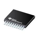
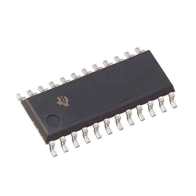
| 供应商器件封装 | 20-TSSOP |
| 元件数 | 1 |
| 其它名称 | 296-33940-5 |
| 包装 | 管件 |
| 单位重量 | 77 mg |
| 商标 | Texas Instruments |
| 安装类型 | 表面贴装 |
| 安装风格 | SMD/SMT |
| 封装 | Tube |
| 封装/外壳 | 20-TSSOP(0.173",4.40mm 宽) |
| 封装/箱体 | TSSOP-20 |
| 工作温度 | -40°C ~ 85°C |
| 工厂包装数量 | 70 |
| 最大工作温度 | + 85 C |
| 最小工作温度 | - 40 C |
| 极性 | Inverting |
| 标准包装 | 70 |
| 每元件位数 | 8 |
| 每芯片的通道数量 | 8 |
| 特性 | 三态 |
| 电压-电源 | 2 V ~ 6 V |
| 电流-输出高,低 | 7.8mA,7.8mA |
| 电流-静态(最大值) | 8µA |
| 电源电压-最大 | 6 V |
| 电源电压-最小 | 2 V |
| 电源电流 | 0.08 mA |
| 电路数 | 1 |
| 系列 | SN74HC540 |
| 输入数 | 8 |
| 输入线路数量 | 8 |
| 输出类型 | 3-State |
| 输出线路数量 | 8 |
| 逻辑电平-低 | 0.5 V ~ 1.8 V |
| 逻辑电平-高 | 1.5 V ~ 4.2 V |
| 逻辑类型 | 缓冲器/线路驱动器, 反相 |
| 逻辑系列 | HC |
| 高电平输出电流 | - 7.8 mA |


PDF Datasheet 数据手册内容提取
(cid:1)(cid:2)(cid:3)(cid:4)(cid:5)(cid:6)(cid:3)(cid:4)(cid:7)(cid:8) (cid:1)(cid:2)(cid:9)(cid:4)(cid:5)(cid:6)(cid:3)(cid:4)(cid:7) (cid:10)(cid:6)(cid:11)(cid:12)(cid:13) (cid:14)(cid:15)(cid:16)(cid:16)(cid:17)(cid:18)(cid:1) (cid:12)(cid:2)(cid:19) (cid:13)(cid:20)(cid:2)(cid:17) (cid:19)(cid:18)(cid:20)(cid:21)(cid:17)(cid:18)(cid:1) (cid:22)(cid:20)(cid:11)(cid:5) (cid:23)(cid:24)(cid:1)(cid:11)(cid:12)(cid:11)(cid:17) (cid:10)(cid:15)(cid:11)(cid:25)(cid:15)(cid:11)(cid:1) SCLS007D − MARCH 1984 − REVISED AUGUST 2003 (cid:1) Wide Operating Voltage Range of 2 V to 6 V SN54HC540...J OR W PACKAGE (cid:1) SN74HC540...DB, DW, N, NS, OR PW PACKAGE High-Current 3-State Outputs Drive Bus (TOP VIEW) Lines Directly or Up To 15 LSTTL Loads (cid:1) Low Power Consumption, 80-µA Max ICC OE1 1 20 VCC (cid:1) Typical tpd = 8 ns A1 2 19 OE2 (cid:1) ±6-mA Output Drive at 5 V A2 3 18 Y1 (cid:1) Low Input Current of 1 µA Max A3 4 17 Y2 A4 5 16 Y3 (cid:1) Data Flow-Through Pinout (All Inputs on A5 6 15 Y4 Opposite Side From Outputs) A6 7 14 Y5 A7 8 13 Y6 description/ordering information A8 9 12 Y7 These octal buffers and line drivers feature the GND 10 11 Y8 performance of the popular ’HC240 series and offer a pinout with inputs and outputs on opposite SN54HC540...FK PACKAGE (TOP VIEW) sides of the package. This arrangement greatly facilitates printed circuit board layout. 1 C2 2 1 E CE A A OV O The 3-state control gate is a 2-input NOR. If either output-enable (OE1 or OE2) input is high, all eight 3 2 1 20 19 A3 4 18 Y1 outputs are in the high-impedance state. The A4 5 17 Y2 ’HC540 devices provide inverted data at the A5 6 16 Y3 outputs. A6 7 15 Y4 A7 8 14 Y5 9 10 1112 13 8D 87 6 AN YY Y G ORDERING INFORMATION ORDERABLE TOP-SIDE TA PACKAGE† PART NUMBER MARKING PDIP − N Tube of 20 SN74HC540N SN74HC540N Tube of 25 SN74HC540DW SSOOIICC −− DDWW HHCC554400 Reel of 2000 SN74HC540DWR SOP − NS Reel of 2000 SN74HC540NSR HC540 −−4400°°CC ttoo 8855°°CC SSOP − DB Reel of 2000 SN74HC540DBR HC540 Tube of 70 SN74HC540PW TTSSSSOOPP −− PPWW Reel of 2000 SN74HC540PWR HHCC554400 Reel of 250 SN74HC540PWT CDIP − J Tube of 20 SNJ54HC540J SNJ54HC540J −−5555°CC ttoo 112255°CC CFP − W Tube of 85 SNJ54HC540W SNJ54HC540W LCCC − FK Tube of 55 SNJ54HC540FK SNJ54HC540FK †Package drawings, standard packing quantities, thermal data, symbolization, and PCB design guidelines are available at www.ti.com/sc/package. Please be aware that an important notice concerning availability, standard warranty, and use in critical applications of TexasInstruments semiconductor products and disclaimers thereto appears at the end of this data sheet. (cid:25)(cid:18)(cid:10)(cid:19)(cid:15)(cid:6)(cid:11)(cid:20)(cid:10)(cid:2) (cid:19)(cid:12)(cid:11)(cid:12) (cid:26)(cid:27)(cid:28)(cid:29)(cid:30)(cid:31)!"(cid:26)(cid:29)(cid:27) (cid:26)# $%(cid:30)(cid:30)&(cid:27)" !# (cid:29)(cid:28) ’%()(cid:26)$!"(cid:26)(cid:29)(cid:27) *!"&+ Copyright 2003, Texas Instruments Incorporated (cid:25)(cid:30)(cid:29)*%$"# $(cid:29)(cid:27)(cid:28)(cid:29)(cid:30)(cid:31) "(cid:29) #’&$(cid:26)(cid:28)(cid:26)$!"(cid:26)(cid:29)(cid:27)# ’&(cid:30) ",& "&(cid:30)(cid:31)# (cid:29)(cid:28) (cid:11)&-!# (cid:20)(cid:27)#"(cid:30)%(cid:31)&(cid:27)"# (cid:10)(cid:27) ’(cid:30)(cid:29)*%$"# $(cid:29)(cid:31)’)(cid:26)!(cid:27)" "(cid:29) 1(cid:20)(cid:13)(cid:24)(cid:25)(cid:18)(cid:16)(cid:24)(cid:23)2(cid:3)(cid:23)(cid:3)(cid:8) !)) ’!(cid:30)!(cid:31)&"&(cid:30)# !(cid:30)& "&#"&* #"!(cid:27)*!(cid:30)* .!(cid:30)(cid:30)!(cid:27)"/+ (cid:25)(cid:30)(cid:29)*%$"(cid:26)(cid:29)(cid:27) ’(cid:30)(cid:29)$&##(cid:26)(cid:27)0 *(cid:29)&# (cid:27)(cid:29)" (cid:27)&$&##!(cid:30)(cid:26))/ (cid:26)(cid:27)$)%*& %(cid:27))&## (cid:29)",&(cid:30).(cid:26)#& (cid:27)(cid:29)"&*+ (cid:10)(cid:27) !)) (cid:29)",&(cid:30) ’(cid:30)(cid:29)*%$"#(cid:8) ’(cid:30)(cid:29)*%$"(cid:26)(cid:29)(cid:27) "&#"(cid:26)(cid:27)0 (cid:29)(cid:28) !)) ’!(cid:30)!(cid:31)&"&(cid:30)#+ ’(cid:30)(cid:29)$&##(cid:26)(cid:27)0 *(cid:29)&# (cid:27)(cid:29)" (cid:27)&$&##!(cid:30)(cid:26))/ (cid:26)(cid:27)$)%*& "&#"(cid:26)(cid:27)0 (cid:29)(cid:28) !)) ’!(cid:30)!(cid:31)&"&(cid:30)#+ POST OFFICE BOX 655303 • DALLAS, TEXAS 75265 1
(cid:1)(cid:2)(cid:3)(cid:4)(cid:5)(cid:6)(cid:3)(cid:4)(cid:7)(cid:8) (cid:1)(cid:2)(cid:9)(cid:4)(cid:5)(cid:6)(cid:3)(cid:4)(cid:7) (cid:10)(cid:6)(cid:11)(cid:12)(cid:13) (cid:14)(cid:15)(cid:16)(cid:16)(cid:17)(cid:18)(cid:1) (cid:12)(cid:2)(cid:19) (cid:13)(cid:20)(cid:2)(cid:17) (cid:19)(cid:18)(cid:20)(cid:21)(cid:17)(cid:18)(cid:1) (cid:22)(cid:20)(cid:11)(cid:5) (cid:23)(cid:24)(cid:1)(cid:11)(cid:12)(cid:11)(cid:17) (cid:10)(cid:15)(cid:11)(cid:25)(cid:15)(cid:11)(cid:1) SCLS007D − MARCH 1984 − REVISED AUGUST 2003 FUNCTION TABLE (each buffer/driver) INPUTS OOUUTTPPUUTT OE1 OE2 A Y L L L H L L H L H X X Z X H X Z logic diagram (positive logic) 1 OE1 19 OE2 2 18 A1 Y1 To Seven Other Channels absolute maximum ratings over operating free-air temperature range (unless otherwise noted)† Supply voltage range, V . . . . . . . . . . . . . . . . . . . . . . . . . . . . . . . . . . . . . . . . . . . . . . . . . . . . . . . . . . −0.5 V to 7 V CC Input clamp current, I (V < 0 or V > V ) (see Note 1) . . . . . . . . . . . . . . . . . . . . . . . . . . . . . . . . . . . . ±20 mA IK I I CC Output clamp current, I (V < 0 or V > V ) (see Note 1) . . . . . . . . . . . . . . . . . . . . . . . . . . . . . . . . ±20 mA OK O O CC Continuous output current, I (V = 0 to V ) . . . . . . . . . . . . . . . . . . . . . . . . . . . . . . . . . . . . . . . . . . . . . . ±35 mA O O CC Continuous current through V or GND . . . . . . . . . . . . . . . . . . . . . . . . . . . . . . . . . . . . . . . . . . . . . . . . . . . ±70 mA CC Package thermal impedance, θJA (see Note 2): DB package . . . . . . . . . . . . . . . . . . . . . . . . . . . . . . . . . 70°C/W DW package . . . . . . . . . . . . . . . . . . . . . . . . . . . . . . . . . 58°C/W N package . . . . . . . . . . . . . . . . . . . . . . . . . . . . . . . . . . . 69°C/W NS package . . . . . . . . . . . . . . . . . . . . . . . . . . . . . . . . . 60°C/W PW package . . . . . . . . . . . . . . . . . . . . . . . . . . . . . . . . . 83°C/W Storage temperature range, T . . . . . . . . . . . . . . . . . . . . . . . . . . . . . . . . . . . . . . . . . . . . . . . . . . . −65°C to 150°C stg †Stresses beyond those listed under “absolute maximum ratings” may cause permanent damage to the device. These are stress ratings only, and functional operation of the device at these or any other conditions beyond those indicated under “recommended operating conditions” is not implied. Exposure to absolute-maximum-rated conditions for extended periods may affect device reliability. NOTES: 1. The input and output voltage ratings may be exceeded if the input and output current ratings are observed. 2. The package thermal impedance is calculated in accordance with JESD 51-7. 2 POST OFFICE BOX 655303 • DALLAS, TEXAS 75265
(cid:1)(cid:2)(cid:3)(cid:4)(cid:5)(cid:6)(cid:3)(cid:4)(cid:7)(cid:8) (cid:1)(cid:2)(cid:9)(cid:4)(cid:5)(cid:6)(cid:3)(cid:4)(cid:7) (cid:10)(cid:6)(cid:11)(cid:12)(cid:13) (cid:14)(cid:15)(cid:16)(cid:16)(cid:17)(cid:18)(cid:1) (cid:12)(cid:2)(cid:19) (cid:13)(cid:20)(cid:2)(cid:17) (cid:19)(cid:18)(cid:20)(cid:21)(cid:17)(cid:18)(cid:1) (cid:22)(cid:20)(cid:11)(cid:5) (cid:23)(cid:24)(cid:1)(cid:11)(cid:12)(cid:11)(cid:17) (cid:10)(cid:15)(cid:11)(cid:25)(cid:15)(cid:11)(cid:1) SCLS007D − MARCH 1984 − REVISED AUGUST 2003 recommended operating conditions (see Note 3) SN54HC540 SN74HC540 UUNNIITT MIN NOM MAX MIN NOM MAX VCC Supply voltage 2 5 6 2 5 6 V VCC = 2 V 1.5 1.5 VVIIHH HHiigghh--lleevveell iinnppuutt vvoollttaaggee VCC = 4.5 V 3.15 3.15 VV VCC = 6 V 4.2 4.2 VCC = 2 V 0.5 0.5 VVIILL LLooww--lleevveell iinnppuutt vvoollttaaggee VCC = 4.5 V 1.35 1.35 VV VCC = 6 V 1.8 1.8 VI Input voltage 0 VCC 0 VCC V VO Output voltage 0 VCC 0 VCC V VCC = 2 V 1000 1000 ∆∆tt//∆∆vv IInnppuutt ttrraannssiittiioonn rriissee//ffaallll ttiimmee VCC = 4.5 V 500 500 nnss VCC = 6 V 400 400 TA Operating free-air temperature −55 125 −40 85 °C NOTE 3: All unused inputs of the device must be held at VCC or GND to ensure proper device operation. Refer to the TI application report, Implications of Slow or Floating CMOS Inputs, literature number SCBA004. electrical characteristics over recommended operating free-air temperature range (unless otherwise noted) TA = 25°C SN54HC540 SN74HC540 PPAARRAAMMEETTEERR TTEESSTT CCOONNDDIITTIIOONNSS VVCCCC UUNNIITT MIN TYP MAX MIN MAX MIN MAX 2 V 1.9 1.998 1.9 1.9 IIOOHH == −−2200 µµAA 4.5 V 4.4 4.499 4.4 4.4 VVOOHH VVII == VVIIHH oorr VVIILL 6 V 5.9 5.999 5.9 5.9 VV IOH = −6 mA 4.5 V 3.98 4.3 3.7 3.84 IOH = −7.8 mA 6 V 5.48 5.8 5.2 5.34 2 V 0.002 0.1 0.1 0.1 IIOOLL == 2200 µµAA 4.5 V 0.001 0.1 0.1 0.1 VVOOLL VVII == VVIIHH oorr VVIILL 6 V 0.001 0.1 0.1 0.1 VV IOL = 6 mA 4.5 V 0.17 0.26 0.4 0.33 IOL = 7.8 mA 6 V 0.15 0.26 0.4 0.33 II VI = VCC or 0 6 V ±0.1 ±100 ±1000 ±1000 nA IOZ VO = VCC or 0 6 V ±0.01 ±0.5 ±10 ±5 µA ICC VI = VCC or 0, IO = 0 6 V 8 160 80 µA Ci 2 V to 6 V 3 10 10 10 pF POST OFFICE BOX 655303 • DALLAS, TEXAS 75265 3
(cid:1)(cid:2)(cid:3)(cid:4)(cid:5)(cid:6)(cid:3)(cid:4)(cid:7)(cid:8) (cid:1)(cid:2)(cid:9)(cid:4)(cid:5)(cid:6)(cid:3)(cid:4)(cid:7) (cid:10)(cid:6)(cid:11)(cid:12)(cid:13) (cid:14)(cid:15)(cid:16)(cid:16)(cid:17)(cid:18)(cid:1) (cid:12)(cid:2)(cid:19) (cid:13)(cid:20)(cid:2)(cid:17) (cid:19)(cid:18)(cid:20)(cid:21)(cid:17)(cid:18)(cid:1) (cid:22)(cid:20)(cid:11)(cid:5) (cid:23)(cid:24)(cid:1)(cid:11)(cid:12)(cid:11)(cid:17) (cid:10)(cid:15)(cid:11)(cid:25)(cid:15)(cid:11)(cid:1) SCLS007D − MARCH 1984 − REVISED AUGUST 2003 switching characteristics over recommended operating free-air temperature range, C = 50 pF L (unless otherwise noted) (see Figure 1) FFRROOMM TTOO TA = 25°C SN54HC540 SN74HC540 PPAARRAAMMEETTEERR (INPUT) (OUTPUT) VVCCCC MIN TYP MAX MIN MAX MIN MAX UUNNIITT 2 V 35 100 149 125 ttppdd AA YY 4.5 V 10 20 30 25 nnss 6 V 8 17 25 21 2 V 75 150 224 188 tteenn OOEE YY 4.5 V 15 30 45 38 nnss 6 V 13 26 38 32 2 V 40 150 224 188 ttddiiss OOEE YY 4.5 V 18 30 45 38 nnss 6 V 17 26 38 32 2 V 28 60 90 75 tttt YY 4.5 V 8 12 18 15 nnss 6 V 6 10 15 13 switching characteristics over recommended operating free-air temperature range, C = 150 pF L (unless otherwise noted) (see Figure 1) FFRROOMM TTOO TA = 25°C SN54HC540 SN74HC540 PPAARRAAMMEETTEERR (INPUT) (OUTPUT) VVCCCC MIN TYP MAX MIN MAX MIN MAX UUNNIITT 2 V 60 150 224 188 ttppdd AA YY 4.5 V 15 30 45 38 nnss 6 V 13 26 38 32 2 V 100 200 298 250 tteenn OOEE YY 4.5 V 20 40 60 50 nnss 6 V 17 34 51 43 2 V 45 210 315 265 tttt YY 4.5 V 17 42 63 53 nnss 6 V 13 36 53 45 operating characteristics, T = 25°C A PARAMETER TEST CONDITIONS TYP UNIT Cpd Power dissipation capacitance per buffer/driver No load 35 pF 4 POST OFFICE BOX 655303 • DALLAS, TEXAS 75265
(cid:1)(cid:2)(cid:3)(cid:4)(cid:5)(cid:6)(cid:3)(cid:4)(cid:7)(cid:8) (cid:1)(cid:2)(cid:9)(cid:4)(cid:5)(cid:6)(cid:3)(cid:4)(cid:7) (cid:10)(cid:6)(cid:11)(cid:12)(cid:13) (cid:14)(cid:15)(cid:16)(cid:16)(cid:17)(cid:18)(cid:1) (cid:12)(cid:2)(cid:19) (cid:13)(cid:20)(cid:2)(cid:17) (cid:19)(cid:18)(cid:20)(cid:21)(cid:17)(cid:18)(cid:1) (cid:22)(cid:20)(cid:11)(cid:5) (cid:23)(cid:24)(cid:1)(cid:11)(cid:12)(cid:11)(cid:17) (cid:10)(cid:15)(cid:11)(cid:25)(cid:15)(cid:11)(cid:1) SCLS007D − MARCH 1984 − REVISED AUGUST 2003 PARAMETER MEASUREMENT INFORMATION VCC PARAMETER RL CL S1 S2 Test S1 ten tPZH 1 kΩ 50o prF Open Closed From Output Point RL tPZL 150 pF Closed Open Under Test tPHZ Open Closed CL tdis 1 kΩ 50 pF (see Note A) S2 tPLZ Closed Open 50 pF tpd or tt −− or Open Open 150 pF LOAD CIRCUIT VCC Input 50% 50% 0 V tPLH tPHL In-Phase VOH 90% 90% Output 50% 50% 10% 10% VOL tr tf Output tPHL tPLH Control VCC VOH (Low-Level 50% 50% Out-of-Phase 90% 50% 50% 90% Enabling) 0 V Output 10% 10% VOL tPZL tPLZ tf tr Output ≈VCC ≈VCC Waveform 1 50% VOLTAGE WAVEFORMS PROPAGATION DELAY AND OUTPUT TRANSITION TIMES (See Note B) 10% VOL tPZH tPHZ VCC Output VOH 90% 90% 90% Input 50% 50% Waveform 2 50% 10% 10% 0 V (See Note B) ≈0 V tr tf VOLTAGE WAVEFORM VOLTAGE WAVEFORMS INPUT RISE AND FALL TIMES ENABLE AND DISABLE TIMES FOR 3-STATE OUTPUTS NOTES: A. CL includes probe and test-fixture capacitance. B. Waveform 1 is for an output with internal conditions such that the output is low except when disabled by the output control. Waveform 2 is for an output with internal conditions such that the output is high except when disabled by the output control. C. Phase relationships between waveforms were chosen arbitrarily. All input pulses are supplied by generators having the following characteristics: PRR ≤ 1 MHz, ZO = 50 Ω, tr = 6 ns, tf = 6 ns. D. The outputs are measured one at a time with one input transition per measurement. E. tPLZ and tPHZ are the same as tdis. F. tPZL and tPZH are the same as ten. G. tPLH and tPHL are the same as tpd. Figure 1. Load Circuit and Voltage Waveforms POST OFFICE BOX 655303 • DALLAS, TEXAS 75265 5
PACKAGE OPTION ADDENDUM www.ti.com 6-Feb-2020 PACKAGING INFORMATION Orderable Device Status Package Type Package Pins Package Eco Plan Lead/Ball Finish MSL Peak Temp Op Temp (°C) Device Marking Samples (1) Drawing Qty (2) (6) (3) (4/5) JM38510/65710BRA ACTIVE CDIP J 20 1 TBD Call TI N / A for Pkg Type -55 to 125 JM38510/ 65710BRA M38510/65710BRA ACTIVE CDIP J 20 1 TBD Call TI N / A for Pkg Type -55 to 125 JM38510/ 65710BRA SN54HC540J ACTIVE CDIP J 20 1 TBD Call TI N / A for Pkg Type -55 to 125 SN54HC540J SN74HC540DW ACTIVE SOIC DW 20 25 Green (RoHS NIPDAU Level-1-260C-UNLIM -40 to 85 HC540 & no Sb/Br) SN74HC540DWE4 ACTIVE SOIC DW 20 25 Green (RoHS NIPDAU Level-1-260C-UNLIM -40 to 85 HC540 & no Sb/Br) SN74HC540DWG4 ACTIVE SOIC DW 20 25 Green (RoHS NIPDAU Level-1-260C-UNLIM -40 to 85 HC540 & no Sb/Br) SN74HC540DWR ACTIVE SOIC DW 20 2000 Green (RoHS NIPDAU Level-1-260C-UNLIM -40 to 85 HC540 & no Sb/Br) SN74HC540DWRE4 ACTIVE SOIC DW 20 2000 Green (RoHS NIPDAU Level-1-260C-UNLIM -40 to 85 HC540 & no Sb/Br) SN74HC540N ACTIVE PDIP N 20 20 Pb-Free NIPDAU N / A for Pkg Type -40 to 85 SN74HC540N (RoHS) SN74HC540NE4 ACTIVE PDIP N 20 20 Pb-Free NIPDAU N / A for Pkg Type -40 to 85 SN74HC540N (RoHS) SN74HC540NSR ACTIVE SO NS 20 2000 Green (RoHS NIPDAU Level-1-260C-UNLIM -40 to 85 HC540 & no Sb/Br) SN74HC540PW ACTIVE TSSOP PW 20 70 Green (RoHS NIPDAU Level-1-260C-UNLIM -40 to 85 HC540 & no Sb/Br) SN74HC540PWR ACTIVE TSSOP PW 20 2000 Green (RoHS NIPDAU Level-1-260C-UNLIM -40 to 85 HC540 & no Sb/Br) SN74HC540PWRE4 ACTIVE TSSOP PW 20 2000 Green (RoHS NIPDAU Level-1-260C-UNLIM -40 to 85 HC540 & no Sb/Br) SN74HC540PWT ACTIVE TSSOP PW 20 250 Green (RoHS NIPDAU Level-1-260C-UNLIM -40 to 85 HC540 & no Sb/Br) SNJ54HC540J ACTIVE CDIP J 20 1 TBD Call TI N / A for Pkg Type -55 to 125 SNJ54HC540J (1) The marketing status values are defined as follows: ACTIVE: Product device recommended for new designs. Addendum-Page 1
PACKAGE OPTION ADDENDUM www.ti.com 6-Feb-2020 LIFEBUY: TI has announced that the device will be discontinued, and a lifetime-buy period is in effect. NRND: Not recommended for new designs. Device is in production to support existing customers, but TI does not recommend using this part in a new design. PREVIEW: Device has been announced but is not in production. Samples may or may not be available. OBSOLETE: TI has discontinued the production of the device. (2) RoHS: TI defines "RoHS" to mean semiconductor products that are compliant with the current EU RoHS requirements for all 10 RoHS substances, including the requirement that RoHS substance do not exceed 0.1% by weight in homogeneous materials. Where designed to be soldered at high temperatures, "RoHS" products are suitable for use in specified lead-free processes. TI may reference these types of products as "Pb-Free". RoHS Exempt: TI defines "RoHS Exempt" to mean products that contain lead but are compliant with EU RoHS pursuant to a specific EU RoHS exemption. Green: TI defines "Green" to mean the content of Chlorine (Cl) and Bromine (Br) based flame retardants meet JS709B low halogen requirements of <=1000ppm threshold. Antimony trioxide based flame retardants must also meet the <=1000ppm threshold requirement. (3) MSL, Peak Temp. - The Moisture Sensitivity Level rating according to the JEDEC industry standard classifications, and peak solder temperature. (4) There may be additional marking, which relates to the logo, the lot trace code information, or the environmental category on the device. (5) Multiple Device Markings will be inside parentheses. Only one Device Marking contained in parentheses and separated by a "~" will appear on a device. If a line is indented then it is a continuation of the previous line and the two combined represent the entire Device Marking for that device. (6) Lead/Ball Finish - Orderable Devices may have multiple material finish options. Finish options are separated by a vertical ruled line. Lead/Ball Finish values may wrap to two lines if the finish value exceeds the maximum column width. Important Information and Disclaimer:The information provided on this page represents TI's knowledge and belief as of the date that it is provided. TI bases its knowledge and belief on information provided by third parties, and makes no representation or warranty as to the accuracy of such information. Efforts are underway to better integrate information from third parties. TI has taken and continues to take reasonable steps to provide representative and accurate information but may not have conducted destructive testing or chemical analysis on incoming materials and chemicals. TI and TI suppliers consider certain information to be proprietary, and thus CAS numbers and other limited information may not be available for release. In no event shall TI's liability arising out of such information exceed the total purchase price of the TI part(s) at issue in this document sold by TI to Customer on an annual basis. OTHER QUALIFIED VERSIONS OF SN54HC540, SN74HC540 : •Catalog: SN74HC540 •Military: SN54HC540 NOTE: Qualified Version Definitions: •Catalog - TI's standard catalog product Addendum-Page 2
PACKAGE OPTION ADDENDUM www.ti.com 6-Feb-2020 •Military - QML certified for Military and Defense Applications Addendum-Page 3
PACKAGE MATERIALS INFORMATION www.ti.com 2-Oct-2019 TAPE AND REEL INFORMATION *Alldimensionsarenominal Device Package Package Pins SPQ Reel Reel A0 B0 K0 P1 W Pin1 Type Drawing Diameter Width (mm) (mm) (mm) (mm) (mm) Quadrant (mm) W1(mm) SN74HC540DWR SOIC DW 20 2000 330.0 24.4 10.8 13.3 2.7 12.0 24.0 Q1 SN74HC540NSR SO NS 20 2000 330.0 24.4 8.4 13.0 2.5 12.0 24.0 Q1 SN74HC540PWR TSSOP PW 20 2000 330.0 16.4 6.95 7.0 1.4 8.0 16.0 Q1 SN74HC540PWT TSSOP PW 20 250 330.0 16.4 6.95 7.1 1.6 8.0 16.0 Q1 PackMaterials-Page1
PACKAGE MATERIALS INFORMATION www.ti.com 2-Oct-2019 *Alldimensionsarenominal Device PackageType PackageDrawing Pins SPQ Length(mm) Width(mm) Height(mm) SN74HC540DWR SOIC DW 20 2000 367.0 367.0 45.0 SN74HC540NSR SO NS 20 2000 367.0 367.0 45.0 SN74HC540PWR TSSOP PW 20 2000 367.0 367.0 38.0 SN74HC540PWT TSSOP PW 20 250 367.0 367.0 38.0 PackMaterials-Page2
None
None
None
None
None
PACKAGE OUTLINE DW0020A SOIC - 2.65 mm max height SCALE 1.200 SOIC C 10.63 SEATING PLANE TYP 9.97 A PIN 1 ID 0.1 C AREA 18X 1.27 20 1 13.0 2X 12.6 11.43 NOTE 3 10 11 0.51 20X 7.6 0.31 2.65 MAX B 7.4 0.25 C A B NOTE 4 0.33 TYP 0.10 0.25 SEE DETAIL A GAGE PLANE 0.3 1.27 0 - 8 0.1 0.40 DETAIL A TYPICAL 4220724/A 05/2016 NOTES: 1. All linear dimensions are in millimeters. Dimensions in parenthesis are for reference only. Dimensioning and tolerancing per ASME Y14.5M. 2. This drawing is subject to change without notice. 3. This dimension does not include mold flash, protrusions, or gate burrs. Mold flash, protrusions, or gate burrs shall not exceed 0.15 mm per side. 4. This dimension does not include interlead flash. Interlead flash shall not exceed 0.43 mm per side. 5. Reference JEDEC registration MS-013. www.ti.com
EXAMPLE BOARD LAYOUT DW0020A SOIC - 2.65 mm max height SOIC 20X (2) SYMM 1 20 20X (0.6) 18X (1.27) SYMM (R0.05) TYP 10 11 (9.3) LAND PATTERN EXAMPLE SCALE:6X SOOPLEDNEINRG MASK METAL MSOELTDAEL RU NMDAESRK SOOPLEDNEINRG MASK 0.07 MAX 0.07 MIN ALL AROUND ALL AROUND NON SOLDER MASK SOLDER MASK DEFINED DEFINED SOLDER MASK DETAILS 4220724/A 05/2016 NOTES: (continued) 6. Publication IPC-7351 may have alternate designs. 7. Solder mask tolerances between and around signal pads can vary based on board fabrication site. www.ti.com
EXAMPLE STENCIL DESIGN DW0020A SOIC - 2.65 mm max height SOIC 20X (2) SYMM 1 20 20X (0.6) 18X (1.27) SYMM 10 11 (9.3) SOLDER PASTE EXAMPLE BASED ON 0.125 mm THICK STENCIL SCALE:6X 4220724/A 05/2016 NOTES: (continued) 8. Laser cutting apertures with trapezoidal walls and rounded corners may offer better paste release. IPC-7525 may have alternate design recommendations. 9. Board assembly site may have different recommendations for stencil design. www.ti.com
IMPORTANTNOTICEANDDISCLAIMER TI PROVIDES TECHNICAL AND RELIABILITY DATA (INCLUDING DATASHEETS), DESIGN RESOURCES (INCLUDING REFERENCE DESIGNS), APPLICATION OR OTHER DESIGN ADVICE, WEB TOOLS, SAFETY INFORMATION, AND OTHER RESOURCES “AS IS” AND WITH ALL FAULTS, AND DISCLAIMS ALL WARRANTIES, EXPRESS AND IMPLIED, INCLUDING WITHOUT LIMITATION ANY IMPLIED WARRANTIES OF MERCHANTABILITY, FITNESS FOR A PARTICULAR PURPOSE OR NON-INFRINGEMENT OF THIRD PARTY INTELLECTUAL PROPERTY RIGHTS. These resources are intended for skilled developers designing with TI products. You are solely responsible for (1) selecting the appropriate TI products for your application, (2) designing, validating and testing your application, and (3) ensuring your application meets applicable standards, and any other safety, security, or other requirements. These resources are subject to change without notice. TI grants you permission to use these resources only for development of an application that uses the TI products described in the resource. Other reproduction and display of these resources is prohibited. No license is granted to any other TI intellectual property right or to any third party intellectual property right. TI disclaims responsibility for, and you will fully indemnify TI and its representatives against, any claims, damages, costs, losses, and liabilities arising out of your use of these resources. TI’s products are provided subject to TI’s Terms of Sale (www.ti.com/legal/termsofsale.html) or other applicable terms available either on ti.com or provided in conjunction with such TI products. TI’s provision of these resources does not expand or otherwise alter TI’s applicable warranties or warranty disclaimers for TI products. Mailing Address: Texas Instruments, Post Office Box 655303, Dallas, Texas 75265 Copyright © 2020, Texas Instruments Incorporated