ICGOO在线商城 > 集成电路(IC) > 逻辑 - 缓冲器,驱动器,接收器,收发器 > SN74AS652DW
 Datasheet下载
- 型号: SN74AS652DW
- 制造商: Texas Instruments
- 库位|库存: xxxx|xxxx
- 要求:
| 数量阶梯 | 香港交货 | 国内含税 |
| +xxxx | $xxxx | ¥xxxx |
查看当月历史价格
查看今年历史价格
SN74AS652DW产品简介:
ICGOO电子元器件商城为您提供SN74AS652DW由Texas Instruments设计生产,在icgoo商城现货销售,并且可以通过原厂、代理商等渠道进行代购。 SN74AS652DW价格参考¥58.85-¥84.86。Texas InstrumentsSN74AS652DW封装/规格:逻辑 - 缓冲器,驱动器,接收器,收发器, Transceiver, Non-Inverting 1 Element 8 Bit per Element 3-State Output 24-SOIC。您可以下载SN74AS652DW参考资料、Datasheet数据手册功能说明书,资料中有SN74AS652DW 详细功能的应用电路图电压和使用方法及教程。
SN74AS652DW是德州仪器(Texas Instruments)生产的逻辑缓冲器、驱动器、接收器和收发器系列中的一款器件。它主要用于高速数据传输和信号调理,适用于多种应用场景。

 应用场景

1. 计算机与外设接口:
   SN74AS652DW常用于计算机系统中的外设接口,如键盘、鼠标、打印机等设备的通信。它可以提供必要的信号增强和电平转换,确保数据在不同电压级别的电路之间可靠传输。

2. 工业控制系统:
   在工业自动化领域,该器件可用于PLC(可编程逻辑控制器)、DCS(分布式控制系统)等设备中。它能够处理来自传感器、执行器和其他控制单元的信号,确保信号的完整性和可靠性,同时减少噪声干扰。

3. 通信设备:
   该器件适用于各种通信设备,如路由器、交换机、调制解调器等。它可以在不同的通信协议之间进行信号转换,确保数据在不同设备之间的稳定传输。

4. 消费电子产品:
   在消费电子领域,SN74AS652DW可以用于电视机、音响、游戏机等设备中。它能够处理音频和视频信号的传输,确保高质量的音视频输出。

5. 汽车电子系统:
   在汽车电子系统中,该器件可用于车载娱乐系统、导航系统、车身控制系统等。它可以处理来自各种传感器和执行器的信号,确保车辆内部各个系统的正常运行。

6. 医疗设备:
   在医疗设备中,SN74AS652DW可以用于心电图机、监护仪等设备中。它能够处理来自传感器的微弱信号,并将其放大和调理,以确保数据的准确性和可靠性。

 特性与优势

- 高速性能:支持高达20MHz的工作频率,适用于高速数据传输应用。
- 低功耗:采用先进的CMOS工艺,具有较低的静态电流消耗,适合电池供电设备。
- 高可靠性:具备较强的抗噪能力和ESD保护,能够在恶劣环境下稳定工作。
- 多路复用:支持多个输入输出通道,简化了电路设计并减少了所需的外部元件数量。

总之,SN74AS652DW凭借其高性能和可靠性,在多个领域得到了广泛应用,特别是在需要高速数据传输和信号调理的应用中表现尤为出色。
| 参数 | 数值 |
| 产品目录 | 集成电路 (IC)半导体 |
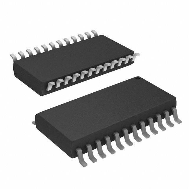
| 描述 | IC BUS TRANSCEIVER DUAL 24SOIC总线收发器 Octal Bus Trncvr/Reg W/3-State Otpt |
| 产品分类 | |
| 品牌 | Texas Instruments |
| 产品手册 | |
| 产品图片 |
|
| rohs | 符合RoHS无铅 / 符合限制有害物质指令(RoHS)规范要求 |
| 产品系列 | 逻辑集成电路,总线收发器,Texas Instruments SN74AS652DW74AS |
| 数据手册 | |
| 产品型号 | SN74AS652DW |
| 产品种类 | 总线收发器 |
| 传播延迟时间 | 9 ns |
| 低电平输出电流 | 48 mA |
| 供应商器件封装 | 24-SOIC |
| 元件数 | 1 |
| 其它名称 | 296-33815-5 |
| 功能 | Bus Transceiver / Register |
| 包装 | 管件 |
| 单位重量 | 624.400 mg |
| 商标 | Texas Instruments |
| 安装类型 | 表面贴装 |
| 安装风格 | SMD/SMT |
| 封装 | Tube |
| 封装/外壳 | 24-SOIC(0.295",7.50mm 宽) |
| 封装/箱体 | SOIC-24 |
| 工作温度 | 0°C ~ 70°C |
| 工厂包装数量 | 25 |
| 最大工作温度 | + 70 C |
| 最小工作温度 | 0 C |
| 极性 | Non-Inverting |
| 标准包装 | 25 |
| 每元件位数 | 8 |
| 每芯片的通道数量 | 8 |
| 电压-电源 | 4.5 V ~ 5.5 V |
| 电流-输出高,低 | 15mA,48mA |
| 电源电压-最大 | 5.5 V |
| 电源电压-最小 | 4.5 V |
| 电路数量 | 8 |
| 系列 | SN74AS652 |
| 输入电平 | TTL |
| 输出电平 | TTL |
| 输出类型 | 3-State |
| 逻辑类型 | Bipolar |
| 逻辑系列 | 74AS |
| 高电平输出电流 | - 15 mA |


- 商务部:美国ITC正式对集成电路等产品启动337调查
- 曝三星4nm工艺存在良率问题 高通将骁龙8 Gen1或转产台积电
- 太阳诱电将投资9.5亿元在常州建新厂生产MLCC 预计2023年完工
- 英特尔发布欧洲新工厂建设计划 深化IDM 2.0 战略
- 台积电先进制程称霸业界 有大客户加持明年业绩稳了
- 达到5530亿美元!SIA预计今年全球半导体销售额将创下新高
- 英特尔拟将自动驾驶子公司Mobileye上市 估值或超500亿美元
- 三星加码芯片和SET,合并消费电子和移动部门,撤换高东真等 CEO
- 三星电子宣布重大人事变动 还合并消费电子和移动部门
- 海关总署:前11个月进口集成电路产品价值2.52万亿元 增长14.8%


PDF Datasheet 数据手册内容提取
SN54ALS652, SN54ALS653, SN54AS651, SN54AS652 SN74ALS651A, SN74ALS652A, SN74ALS653, SN74ALS654, SN74AS651, SN74AS652 OCTAL BUS TRANSCEIVERS AND REGISTERS WITH 3-STATE OUTPUTS SDAS066G – DECEMBER 1983 – REVISED DECEMBER 2000 (cid:0) Bus Transceivers/Registers SN54ALS’, SN54AS’...JT PACKAGE (cid:0) SN74ALS’, SN74AS’...DW OR NT PACKAGE Independent Registers and Enables for A (TOP VIEW) and B Buses (cid:0) Multiplexed Real-Time and Stored Data CLKAB 1 24 VCC (cid:0) Choice of True or Inverting Data Paths SAB 2 23 CLKBA (cid:0) OEAB 3 22 SBA Choice of 3-State or Open-Collector A1 4 21 OEBA Outputs to A Bus A2 5 20 B1 A3 6 19 B2 DEVICE A OUTPUT B OUTPUT LOGIC A4 7 18 B3 SN74ALS651A, 3-State 3-State Inverting A5 8 17 B4 ’AS651 A6 9 16 B5 SN54ALS652, A7 10 15 B6 SN74ALS652A, 3-State 3-State True ’AS652 A8 11 14 B7 GND 12 13 B8 ’ALS653 Open Collector 3-State Inverting SN74ALS654 Open Collector 3-State True SN54ALS’, SN54AS’...FK PACKAGE description (TOP VIEW) B A These devices consist of bus-transceiver circuits, B A B AB K CK B D-type flip-flops, and control circuitry arranged for EA L C CL A OS C NV C S multiplexed transmission of data directly from the data bus or from the internal storage registers. 4 3 2 1 28 27 26 Output-enable (OEAB and OEBA) inputs are A1 5 25 OEBA provided to control the transceiver functions. A2 6 24 B1 Select-control (SAB and SBA) inputs are provided A3 7 23 B2 to select real-time or stored data transfer. The NC 8 22 NC circuitry used for select control eliminates the A4 9 21 B3 typical decoding glitch that occurs in a multiplexer A5 10 20 B4 during the transition between stored and real-time A6 11 19 B5 data. A low input level selects real-time data, and 12 1314 15 16 1718 a high input level selects stored data. Figure 1 7 8 D C 8 76 illustrates the four fundamental bus-management A A N N B BB G functions that can be performed with the octal bus transceivers and registers NC – No internal connection Data on the A or B data bus, or both, can be stored in the internal D-type flip-flops by low-to-high transitions at the appropriate clock (CLKAB or CLKBA) terminals, regardless of the select- or output-control terminals. When SAB and SBA are in the real-time transfer mode, it is possible to store data without using the internal D-type flip-flops by simultaneously enabling OEAB and OEBA. In this configuration, each output reinforces its input. When all other data sources to the two sets of bus lines are at high impedance, each set of bus lines remains at its last state. The -1 versions of the SN74ALS651A and SN74ALS652A are identical to the standard versions except that the recommended maximum I for the -1 versions is increased to 48 mA. There are no -1 versions of the OL SN54ALS652, SN54ALS653, SN74ALS653, and SN74ALS654. Please be aware that an important notice concerning availability, standard warranty, and use in critical applications of TexasInstruments semiconductor products and disclaimers thereto appears at the end of this data sheet. PRODUCTION DATA information is current as of publication date. Copyright 2000, Texas Instruments Incorporated Products conform to specifications per the terms of Texas Instruments standard warranty. Production processing does not necessarily include testing of all parameters. POST OFFICE BOX 655303 • DALLAS, TEXAS 75265 1
SN54ALS652, SN54ALS653, SN54AS651, SN54AS652 SN74ALS651A, SN74ALS652A, SN74ALS653, SN74ALS654, SN74AS651, SN74AS652 OCTAL BUS TRANSCEIVERS AND REGISTERS WITH 3-STATE OUTPUTS SDAS066G – DECEMBER 1983 – REVISED DECEMBER 2000 ORDERING INFORMATION ORDERABLE TOP-SIDE TA PACKAGE† PART NUMBER MARKING SN74ALS651ANT SN74ALS651ANT SN74ALS652ANT SN74ALS652ANT SN74ALS653NT SN74ALS653NT PPDDIIPP – NNTT TTuubbee SN74ALS654NT SN74ALS654NT SN74AS651NT SN74AS651NT SN74AS652NT SN74AS652NT Tube SN74ALS651ADW AALLSS665511AA Tape and reel SN74ALS651ADWR Tube SN74ALS652ADW 00°°CC ttoo 7700°°CC AALLSS665522AA Tape and reel SN74ALS652ADWR Tube SN74ALS653DW AALLSS665533 Tape and reel SN74ALS653DWR SSOOIICC – DDWW Tube SN74ALS654DW AALLSS665544 Tape and reel SN74ALS654DWR Tube SN74AS651DW AASS665511 Tape and reel SN74AS651DWR Tube SN74AS652DW AASS665522 Tape and reel SN74AS652DWR SNJ54ALS652JT SNJ54ALS652JT SNJ54ALS653JT SNJ54ALS653JT CCDDIIPP – JJTT TTuubbee SNJ54AS651JT SNJ54AS651JT SNJ54AS652JT SNJ54AS652JT –5555°°CC ttoo 112255°°CC SNJ54ALS652FK SNJ54ALS652FK SNJ54ALS653FK SNJ54ALS653FK LLCCCCCC – FFKK TTuubbee SNJ54AS651FK SNJ54AS651FK SNJ54AS652FK SNJ54AS652FK †Package drawings, standard packing quantities, thermal data, symbolization, and PCB design guidelines are available at www.ti.com/sc/package. 2 POST OFFICE BOX 655303 • DALLAS, TEXAS 75265
SN54ALS652, SN54ALS653, SN54AS651, SN54AS652 SN74ALS651A, SN74ALS652A, SN74ALS653, SN74ALS654, SN74AS651, SN74AS652 OCTAL BUS TRANSCEIVERS AND REGISTERS WITH 3-STATE OUTPUTS SDAS066G – DECEMBER 1983 – REVISED DECEMBER 2000 A B A B S S S S U U U U B B B B 3 21 1 23 2 22 3 21 1 23 2 22 OEAB OEBA CLKAB CLKBA SAB SBA OEAB OEBA CLKAB CLKBA SAB SBA L L X X X L H H X X L X REAL-TIME TRANSFER REAL-TIME TRANSFER BUS B TO BUS A BUS A TO BUS B A B A B S S S S U U U U B B B B 3 21 1 23 2 22 3 21 1 23 2 22 OEAB OEBA CLKAB CLKBA SAB SBA OEAB OEBA CLKAB CLKBA SAB SBA X H ↑ X X X H L H or L H or L H H L X X ↑ X X L H ↑ ↑ X X STORAGE FROM TRANSFER STORED DATA A, B, OR A AND B TO A AND/OR B Pin numbers shown are for the DW, JT, and NT packages. Figure 1. Bus-Management Functions POST OFFICE BOX 655303 • DALLAS, TEXAS 75265 3
SN54ALS652, SN54ALS653, SN54AS651, SN54AS652 SN74ALS651A, SN74ALS652A, SN74ALS653, SN74ALS654, SN74AS651, SN74AS652 OCTAL BUS TRANSCEIVERS AND REGISTERS WITH 3-STATE OUTPUTS SDAS066G – DECEMBER 1983 – REVISED DECEMBER 2000 Function Tables SN54ALS653, SN54AS651, SN74ALS651A, SN74ALS653, SN74AS651 INPUTS DATA I/O† OOPPEERRAATTIIOONN OORR FFUUNNCCTTIIOONN OEAB OEBA CLKAB CLKBA SAB SBA A1–A8 B1–B8 L H H or L H or L X X Input Input Isolation L H ↑ ↑ X X Input Input Store A and B data X H ↑ H or L X X Input Unspecified‡ Store A, hold B H H ↑ ↑ X‡ X Input Output Store A in both registers L X H or L ↑ X X Unspecified‡ Input Hold A, store B L L ↑ ↑ X X‡ Output Input Store B in both registers L L X X X L Output Input Real-time B data to A bus L L X H or L X H Output Input Stored B data to A bus H H X X L X Input Output Real-time A data to B bus H H H or L X H X Input Output Stored A data to B bus Stored A data to B bus and H L H or L H or L H H Output Output stored B data to A bus †The data output functions can be enabled or disabled by a variety of level combinations at OEAB or OEBA. Data input functions always are enabled; i.e., data at the bus terminals is stored on every low-to-high transition on the clock inputs. ‡Select control = L: clocks can occur simultaneously. Select control = H: clocks must be staggered to load both registers. SN54ALS652, SN54AS652, SN74ALS652A, SN74ALS654, SN74AS652 INPUTS DATA I/O† OOPPEERRAATTIIOONN OORR FFUUNNCCTTIIOONN OEAB OEBA CLKAB CLKBA SAB SBA A1–A8 B1–B8 L H H or L H or L X X Input Input Isolation L H ↑ ↑ X X Input Input Store A and B data X H ↑ H or L X X Input Unspecified‡ Store A, hold B H H ↑ ↑ X‡ X Input Output Store A in both registers L X H or L ↑ X X Unspecified‡ Input Hold A, store B L L ↑ ↑ X X‡ Output Input Store B in both registers L L X X X L Output Input Real-time B data to A bus L L X H or L X H Output Input Stored B data to A bus H H X X L X Input Output Real-time A data to B bus H H H or L X H X Input Output Stored A data to B bus Stored A data to B bus and H L H or L H or L H H Output Output stored B data to A bus †The data output functions can be enabled or disabled by a variety of level combinations at OEAB or OEBA. Data input functions always are enabled; i.e., data at the bus terminals is stored on every low-to-high transition on the clock inputs. ‡Select control = L: clocks can occur simultaneously. Select control = H: clocks must be staggered to load both registers. 4 POST OFFICE BOX 655303 • DALLAS, TEXAS 75265
SN54ALS652, SN54ALS653, SN54AS651, SN54AS652 SN74ALS651A, SN74ALS652A, SN74ALS653, SN74ALS654, SN74AS651, SN74AS652 OCTAL BUS TRANSCEIVERS AND REGISTERS WITH 3-STATE OUTPUTS SDAS066G – DECEMBER 1983 – REVISED DECEMBER 2000 logic symbols† SN54AS651, SN54ALS652, SN54AS652, SN74ALS651A, SN74AS651 SN74ALS652A, SN74AS652 21 21 OEBA EN1 [BA] OEBA EN1 [BA] 3 3 OEAB EN2 [AB] OEAB EN2 [AB] 23 23 CLKBA C4 CLKBA C4 22 22 SBA G5 SBA G5 1 1 CLKAB C6 CLKAB C6 2 2 SAB G7 SAB G7 20 20 4 ≥1 5 4D B1 4 ≥1 5 4D B1 A1 1 A1 1 5 1 5 1 6D 7 ≥1 6D 7 ≥1 2 2 1 7 1 7 5 19 5 19 A2 B2 A2 B2 6 18 6 18 A3 B3 A3 B3 7 17 7 17 A4 B4 A4 B4 8 16 8 16 A5 B5 A5 B5 9 15 9 15 A6 B6 A6 B6 10 14 10 14 A7 B7 A7 B7 11 13 11 13 A8 B8 A8 B8 SN54ALS653, SN74ALS653 SN74ALS654 21 21 OEBA EN1 [BA] OEBA EN1 [BA] 3 3 OEAB EN2 [AB] OEAB EN2 [AB] 23 23 CLKBA C4 CLKBA C4 22 22 SBA G5 SBA G5 1 1 CLKAB C6 CLKAB C6 2 2 SAB G7 SAB G7 20 20 4 ≥1 5 4D B1 4 ≥1 5 4D B1 A1 1 A1 1 5 1 5 1 6D 7 ≥1 6D 7 ≥1 2 2 1 7 1 7 5 19 5 19 A2 B2 A2 B2 6 18 6 18 A3 B3 A3 B3 7 17 7 17 A4 B4 A4 B4 8 16 8 16 A5 B5 A5 B5 9 15 9 15 A6 B6 A6 B6 10 14 10 14 A7 B7 A7 B7 11 13 11 13 A8 B8 A8 B8 †These symbols are in accordance with ANSI/IEEE Std 91-1984 and IEC Publication 617-12. Pin numbers shown are for the DW, JT, and NT packages. POST OFFICE BOX 655303 • DALLAS, TEXAS 75265 5
SN54ALS652, SN54ALS653, SN54AS651, SN54AS652 SN74ALS651A, SN74ALS652A, SN74ALS653, SN74ALS654, SN74AS651, SN74AS652 OCTAL BUS TRANSCEIVERS AND REGISTERS WITH 3-STATE OUTPUTS SDAS066G – DECEMBER 1983 – REVISED DECEMBER 2000 logic diagrams (positive logic) 21 OEBA SN54ALS653, SN54AS651, SN74ALS651A, SN74ALS653, SN74AS651 3 OEAB 23 CLKBA 22 SBA 1 CLKAB 2 SAB One of Eight Channels 1D C1 4 A1 20 B1 1D C1 To Seven Other Channels 21 OEBA SN54ALS652, SN54AS652, SN74ALS652A, SN74ALS654, SN74AS652 3 OEAB 23 CLKBA 22 SBA 1 CLKAB 2 SAB One of Eight Channels 1D C1 4 A1 20 B1 1D C1 To Seven Other Channels Pin numbers shown are for the DW, JT, and NT packages. 6 POST OFFICE BOX 655303 • DALLAS, TEXAS 75265
SN54ALS652, SN54ALS653, SN54AS651, SN54AS652 SN74ALS651A, SN74ALS652A, SN74ALS653, SN74ALS654, SN74AS651, SN74AS652 OCTAL BUS TRANSCEIVERS AND REGISTERS WITH 3-STATE OUTPUTS SDAS066G – DECEMBER 1983 – REVISED DECEMBER 2000 absolute maximum ratings over operating free-air temperature range (unless otherwise noted)† Supply voltage range, V . . . . . . . . . . . . . . . . . . . . . . . . . . . . . . . . . . . . . . . . . . . . . . . . . . . . . . . . . . –0.5 V to 7 V CC Input voltage range, V: Control inputs . . . . . . . . . . . . . . . . . . . . . . . . . . . . . . . . . . . . . . . . . . . . . . . . –0.5 V to 7 V I I/O ports . . . . . . . . . . . . . . . . . . . . . . . . . . . . . . . . . . . . . . . . . . . . . . . . . . . –0.5 V to 5.5 V Package thermal impedance, θ (see Note 1): DW package . . . . . . . . . . . . . . . . . . . . . . . . . . . . . . . . . 46°C/W JA NT package . . . . . . . . . . . . . . . . . . . . . . . . . . . . . . . . . 67°C/W Storage temperature range, T . . . . . . . . . . . . . . . . . . . . . . . . . . . . . . . . . . . . . . . . . . . . . . . . . . –65°C to 150°C stg †Stresses beyond those listed under “absolute maximum ratings” may cause permanent damage to the device. These are stress ratings only, and functional operation of the device at these or any other conditions beyond those indicated under “recommended operating conditions” is not implied. Exposure to absolute-maximum-rated conditions for extended periods may affect device reliability. NOTE 1: The package thermal impedance is calculated in accordance with JESD 51. recommended operating conditions SN74ALS651A UUNNIITT MIN NOM MAX VCC Supply voltage 4.5 5 5.5 V VIH High-level input voltage 2 V VIL Low-level input voltage 0.8 V IOH High-level output current –15 mA 24 IIOL LLooww-lleevveell oouuttppuutt ccuurrrreenntt 48‡ mmAA fclock Clock frequency 0 40 MHz CLKBA or CLKAB high 12.5 ttw PPuullssee dduurraattiioonn nnss CLKBA or CLKAB low 12.5 tsu Setup time before CLKAB↑ or CLKBA↑ A or B 10 ns th Hold time after CLKAB↑ or CLKBA↑ A or B 0 ns TA Operating free-air temperature 0 70 °C ‡Applies only to the SN74ALS651A-1 and only if VCC is maintained between 4.75 V and 5.25 V recommended operating conditions SN54ALS652 SN74ALS652A UUNNIITT MIN NOM MAX MIN NOM MAX VCC Supply voltage 4.5 5 5.5 4.5 5 5.5 V VIH High-level input voltage 2 2 V VIL Low-level input voltage 0.7 0.8 V IOH High-level output current –12 –15 mA 12 24 IIOL LLooww-lleevveell oouuttppuutt ccuurrrreenntt 48‡ mmAA fclock Clock frequency 0 35 0 40 MHz CLKBA or CLKAB high 14.5 12.5 ttw PPuullssee dduurraattiioonn nnss CLKBA or CLKAB low 14.5 12.5 tsu Setup time before CLKAB↑ or CLKBA↑ A or B 15 10 ns th Hold time after CLKAB↑ or CLKBA↑ A or B 5 0 ns TA Operating free-air temperature –55 125 0 70 °C ‡Applies only to the SN74ALS652A-1 and only if VCC is maintained between 4.75 V and 5.25 V POST OFFICE BOX 655303 • DALLAS, TEXAS 75265 7
SN54ALS652, SN54ALS653, SN54AS651, SN54AS652 SN74ALS651A, SN74ALS652A, SN74ALS653, SN74ALS654, SN74AS651, SN74AS652 OCTAL BUS TRANSCEIVERS AND REGISTERS WITH 3-STATE OUTPUTS SDAS066G – DECEMBER 1983 – REVISED DECEMBER 2000 electrical characteristics over recommended operating free-air temperature range (unless otherwise noted) SN74ALS651A PPAARRAAMMEETTEERR TTEESSTT CCOONNDDIITTIIOONNSS UUNNIITT MIN TYP† MAX VIK VCC = 4.5 V, II = –18 mA –1.2 V VCC = 4.5 V to 5.5 V, IOH = –0.4 mA VCC–2 VOH IOH = –3 mA 2.4 3.2 V VVCCCC == 44.55 VV IOH = –15 mA 2 IOL = 12 mA 0.25 0.4 VVCCCC == 44.55 VV VOL IOL = 24 mA 0.35 0.5 V VCC = 4.75 V, IOL = 48 mA (-1 versions) 0.35 0.5 Control inputs VCC = 5.5 V, VI = 7 V 0.1 IIII mmAA A or B ports VCC = 5.5 V, VI = 5.5 V 0.1 Control inputs 20 IIIH A or B ports‡ VVCC = 55.55 VV, VVI = 22.77 VV 20 µAA Control inputs –0.2 IIIL A or B ports‡ VVCC = 55.55 VV, VVI = 00.44 VV –0.2 mmAA IO§ VCC = 5.5 V, VO = 2.25 V –30 –112 mA Outputs high 42 68 ICC VCC = 5.5 V Outputs low 52 82 mA Outputs disabled 52 82 †All typical values are at VCC = 5 V, TA = 25°C. ‡For I/O ports, the parameters IIH and IIL include the off-state output current. §The output conditions have been chosen to produce a current that closely approximates one-half of the true short-circuit output current, IOS. 8 POST OFFICE BOX 655303 • DALLAS, TEXAS 75265
SN54ALS652, SN54ALS653, SN54AS651, SN54AS652 SN74ALS651A, SN74ALS652A, SN74ALS653, SN74ALS654, SN74AS651, SN74AS652 OCTAL BUS TRANSCEIVERS AND REGISTERS WITH 3-STATE OUTPUTS SDAS066G – DECEMBER 1983 – REVISED DECEMBER 2000 electrical characteristics over recommended operating free-air temperature range (unless otherwise noted) SN54ALS652 SN74ALS652A PPAARRAAMMEETTEERR TTEESSTT CCOONNDDIITTIIOONNSS UUNNIITT MIN TYP† MAX MIN TYP† MAX VIK VCC = 4.5 V, II = –18 mA –1.2 –1.2 V VCC = 4.5 V to 5.5 V, IOH = –0.4 mA VCC–2 VCC–2 IOH = –3 mA 2.4 3.2 2.4 3.2 VVOOHH VV VCC = 4.5 V IOH = –12 mA 2 IOH = –15 mA 2 IOL = 12 mA 0.25 0.4 0.25 0.4 VVCCCC == 44.55 VV VOL IOL = 24 mA 0.35 0.5 V VCC = 4.75 V, IOL = 48 mA (-1 versions) 0.35 0.5 Control inputs VCC = 5.5 V, VI = 7 V 0.1 0.1 IIII mmAA A or B ports VCC = 5.5 V, VI = 5.5 V 0.1 0.1 Control inputs 20 20 IIIH A or B ports‡ VVCC = 55.55 VV, VVI = 22.77 VV 20 20 µAA Control inputs –0.2 –0.2 IIIL A or B ports‡ VVCC = 55.55 VV, VVI = 00.44 VV –0.2 –0.2 mmAA IO§ VCC = 5.5 V, VO = 2.25 V –20 –112 –30 –112 mA Outputs high 47 76 47 76 ICC VCC = 5.5 V Outputs low 55 88 55 88 mA Outputs disabled 55 88 55 88 †All typical values are at VCC = 5 V, TA = 25°C. ‡For I/O ports, the parameters IIH and IIL include the off-state output current. §The output conditions have been chosen to produce a current that closely approximates one-half of the true short-circuit output current, IOS. POST OFFICE BOX 655303 • DALLAS, TEXAS 75265 9
SN54ALS652, SN54ALS653, SN54AS651, SN54AS652 SN74ALS651A, SN74ALS652A, SN74ALS653, SN74ALS654, SN74AS651, SN74AS652 OCTAL BUS TRANSCEIVERS AND REGISTERS WITH 3-STATE OUTPUTS SDAS066G – DECEMBER 1983 – REVISED DECEMBER 2000 switching characteristics (see Figure 2) VCC = 4.5 V to 5.5 V, CL = 50 pF, R1 = 500 Ω, FROM TO R2 = 500 Ω, PARAMETER UNIT (INPUT) (OUTPUT) TA = MIN to MAX† SN74ALS651A MIN MAX fmax 40 MHz tPLH 8 32 CCLLKKBBAA oorr CCLLKKAABB AA oorr BB nnss tPHL 5 17 tPLH 2 18 AA oorr BB BB oorr AA nnss tPHL 2 10 tPLH SBA or SAB‡ 8 38 AA oorr BB nnss tPHL (with A or B high) 6 21 tPLH SBA or SAB‡ 8 25 AA oorr BB nnss tPHL (with A or B low) 7 21 tPZH 3 20 OOEEBBAA AA nnss tPZL 5 18 tPHZ 2 9 OOEEBBAA AA nnss tPLZ 3 12 tPZH 3 22 OOEEAABB BB nnss tPZL 6 21 tPHZ 2 12 OOEEAABB BB nnss tPLZ 2 14 †For conditions shown as MIN or MAX, use the appropriate value specified under recommended operating conditions. ‡These parameters are measured with the internal output state of the storage register opposite that of the bus input. 10 POST OFFICE BOX 655303 • DALLAS, TEXAS 75265
SN54ALS652, SN54ALS653, SN54AS651, SN54AS652 SN74ALS651A, SN74ALS652A, SN74ALS653, SN74ALS654, SN74AS651, SN74AS652 OCTAL BUS TRANSCEIVERS AND REGISTERS WITH 3-STATE OUTPUTS SDAS066G – DECEMBER 1983 – REVISED DECEMBER 2000 switching characteristics (see Figure 2) VCC = 4.5 V to 5.5 V, CL = 50 pF, R1 = 500 Ω, FROM TO R2 = 500 Ω, PARAMETER UNIT (INPUT) (OUTPUT) TA = MIN to MAX† SN54ALS652 SN74ALS652A MIN MAX MIN MAX fmax 35 40 MHz tPLH 10 35 8 30 CCLLKKBBAA oorr CCLLKKAABB AA oorr BB nnss tPHL 5 20 5 17 tPLH 5 20 4 18 AA oorr BB BB oorr AA nnss tPHL 3 15 3 12 tPLH SSBBAA oorr SSAABB‡ 15 40 8 35 AA oorr BB nnss tPHL (with A or B high) 6 23 6 20 tPLH SSBBAA oorr SSAABB‡ 8 30 8 25 AA oorr BB nnss tPHL (with A or B low) 5 24 5 20 tPZH 3 20 3 17 OOEEBBAA AA nnss tPZL 5 22 5 18 tPHZ 1 12 1 10 OOEEBBAA AA nnss tPLZ 2 20 2 16 tPZH 8 25 3 22 OOEEAABB BB nnss tPZL 6 21 5 18 tPHZ 1 12 1 10 OOEEAABB BB nnss tPLZ 2 21 2 16 †For conditions shown as MIN or MAX, use the appropriate value specified under recommended operating conditions. ‡These parameters are measured with the internal output state of the storage register opposite that of the bus input. POST OFFICE BOX 655303 • DALLAS, TEXAS 75265 11
SN54ALS652, SN54ALS653, SN54AS651, SN54AS652 SN74ALS651A, SN74ALS652A, SN74ALS653, SN74ALS654, SN74AS651, SN74AS652 OCTAL BUS TRANSCEIVERS AND REGISTERS WITH 3-STATE OUTPUTS SDAS066G – DECEMBER 1983 – REVISED DECEMBER 2000 absolute maximum ratings over operating free-air temperature range (unless otherwise noted)† Supply voltage range, V . . . . . . . . . . . . . . . . . . . . . . . . . . . . . . . . . . . . . . . . . . . . . . . . . . . . . . . . . . –0.5 V to 7 V CC Input voltage range, V: Control inputs . . . . . . . . . . . . . . . . . . . . . . . . . . . . . . . . . . . . . . . . . . . . . . . . –0.5 V to 7 V I I/O ports . . . . . . . . . . . . . . . . . . . . . . . . . . . . . . . . . . . . . . . . . . . . . . . . . . . –0.5 V to 5.5 V Package thermal impedance, θ (see Note 1): DW package . . . . . . . . . . . . . . . . . . . . . . . . . . . . . . . . . 46°C/W JA NT package . . . . . . . . . . . . . . . . . . . . . . . . . . . . . . . . . 67°C/W Storage temperature range, T . . . . . . . . . . . . . . . . . . . . . . . . . . . . . . . . . . . . . . . . . . . . . . . . . . –65°C to 150°C stg †Stresses beyond those listed under “absolute maximum ratings” may cause permanent damage to the device. These are stress ratings only, and functional operation of the device at these or any other conditions beyond those indicated under “recommended operating conditions” is not implied. Exposure to absolute-maximum-rated conditions for extended periods may affect device reliability. NOTE 1: The package thermal impedance is calculated in accordance with JESD 51. recommended operating conditions SN54ALS653 SN74ALS653 UUNNIITT MIN NOM MAX MIN NOM MAX VCC Supply voltage 4.5 5 5.5 4.5 5 5.5 V VIH High-level input voltage 2 2 V VIL Low-level input voltage 0.7 0.8 V VOH High-level output voltage A ports 5.5 5.5 V IOH High-level output current B ports –12 –15 mA IOL Low-level output current 12 24 mA fclock Clock frequency 0 25 0 35 MHz CLKBA or CLKAB high 20 14.5 ttw PPuullssee dduurraattiioonn nnss CLKBA or CLKAB low 20 14.5 tsu Setup time before CLKAB↑ or CLKBA↑ A or B 15 10 ns th Hold time after CLKAB↑ or CLKBA↑ A or B 5 0 ns TA Operating free-air temperature –55 125 0 70 °C recommended operating conditions SN74ALS654 UUNNIITT MIN NOM MAX VCC Supply voltage 4.5 5 5.5 V VIH High-level input voltage 2 V VIL Low-level input voltage 0.8 V VOH High-level output voltage A ports 5.5 V IOH High-level output current B ports –15 mA IOL Low-level output current 24 mA fclock Clock frequency 0 35 MHz CLKBA or CLKAB high 14.5 ttw PPuullssee dduurraattiioonn nnss CLKBA or CLKAB low 14.5 tsu Setup time before CLKAB↑ or CLKBA↑ A or B 10 ns th Hold time after CLKAB↑ or CLKBA↑ A or B 0 ns TA Operating free-air temperature 0 70 °C 12 POST OFFICE BOX 655303 • DALLAS, TEXAS 75265
SN54ALS652, SN54ALS653, SN54AS651, SN54AS652 SN74ALS651A, SN74ALS652A, SN74ALS653, SN74ALS654, SN74AS651, SN74AS652 OCTAL BUS TRANSCEIVERS AND REGISTERS WITH 3-STATE OUTPUTS SDAS066G – DECEMBER 1983 – REVISED DECEMBER 2000 electrical characteristics over recommended operating free-air temperature range (unless otherwise noted) SN54ALS653 SN74ALS653 PPAARRAAMMEETTEERR TTEESSTT CCOONNDDIITTIIOONNSS UUNNIITT MIN TYP† MAX MIN TYP† MAX VIK VCC = 4.5 V, II = –18 mA –1.2 –1.2 V VCC = 4.5 V to 5.5 V, IOH = –0.4 mA VCC–2 VCC–2 IOH = –3 mA 2.4 3.2 2.4 3.2 VVOOHH BB ppoorrttss VV VCC = 4.5 V IOH = –12 mA 2 IOH = –15 mA 2 IOL = 12 mA 0.25 0.4 0.25 0.4 VVOOLL VVCCCC == 44.55 VV VV IOL = 24 mA 0.35 0.5 Control inputs VCC = 5.5 V, VI = 7 V 0.1 0.1 IIII mmAA A or B ports VCC = 5.5 V, VI = 5.5 V 0.1 0.1 Control inputs 20 20 IIIH A or B ports‡ VVCC = 55.55 VV, VVI = 22.77 VV 20 20 µAA Control inputs –0.2 –0.2 IIIL A or B ports‡ VVCC = 55.55 VV, VVI = 00.44 VV –0.2 –0.2 mmAA IOH A ports VCC = 4.5 V, VOH = 5.5 V 0.1 0.1 mA IO§ B ports VCC = 5.5 V, VO = 2.25 V –20 –112 –30 –112 mA Outputs high 47 76 47 76 ICC VCC = 5.5 V Outputs low 55 88 55 88 mA Outputs disabled 55 88 55 88 †All typical values are at VCC = 5 V, TA = 25°C. ‡For I/O ports, the parameters IIH and IIL include the off-state output current. §The output conditions have been chosen to produce a current that closely approximates one-half of the true short-circuit output current, IOS. POST OFFICE BOX 655303 • DALLAS, TEXAS 75265 13
SN54ALS652, SN54ALS653, SN54AS651, SN54AS652 SN74ALS651A, SN74ALS652A, SN74ALS653, SN74ALS654, SN74AS651, SN74AS652 OCTAL BUS TRANSCEIVERS AND REGISTERS WITH 3-STATE OUTPUTS SDAS066G – DECEMBER 1983 – REVISED DECEMBER 2000 electrical characteristics over recommended operating free-air temperature range (unless otherwise noted) SN74ALS654 PPAARRAAMMEETTEERR TTEESSTT CCOONNDDIITTIIOONNSS UUNNIITT MIN TYP† MAX VIK VCC = 4.5 V, II = –18 mA –1.2 V VCC = 4.5 V to 5.5 V, IOH = –0.4 mA VCC–2 VOH B ports IOH = –3 mA 2.4 3.2 V VVCCCC == 44.55 VV IOH = –15 mA 2 IOL = 12 mA 0.25 0.4 VVOOLL VVCCCC == 44.55 VV VV IOL = 24 mA 0.35 0.5 Control inputs VCC = 5.5 V, VI = 7 V 0.1 IIII mmAA A or B ports VCC = 5.5 V, VI = 5.5 V 0.1 Control inputs 20 IIIIHH A or B ports‡ VVCCCC == 55.55 VV, VVII == 22.77 VV 20 µµAA Control inputs –0.2 IIIILL A or B ports‡ VVCCCC == 55.55 VV, VVII == 00.44 VV –0.2 mmAA IOH A ports VCC = 4.5 V, VOH = 5.5 V 0.1 mA IO§ B ports VCC = 5.5 V, VO = 2.25 V –30 –112 mA Outputs high 47 76 ICC VCC = 5.5 V Outputs low 55 88 mA Outputs disabled 55 88 †All typical values are at VCC = 5 V, TA = 25°C. ‡For I/O ports, the parameters IIH and IIL include the off-state output current. §The output conditions have been chosen to produce a current that closely approximates one-half of the true short-circuit output current, IOS. 14 POST OFFICE BOX 655303 • DALLAS, TEXAS 75265
SN54ALS652, SN54ALS653, SN54AS651, SN54AS652 SN74ALS651A, SN74ALS652A, SN74ALS653, SN74ALS654, SN74AS651, SN74AS652 OCTAL BUS TRANSCEIVERS AND REGISTERS WITH 3-STATE OUTPUTS SDAS066G – DECEMBER 1983 – REVISED DECEMBER 2000 switching characteristics (see Figure 2) VCC = 4.5 V to 5.5 V, CL = 50 pF, RL = 680 Ω (A outputs), FROM TO R1 = R2 = 500 Ω (B outputs), PARAMETER UNIT (INPUT) (OUTPUT) TA = MIN to MAX† SN54ALS653 SN74ALS653 MIN MAX MIN MAX fmax 25 35 MHz tPLH 16 71 16 64 CCLLKKBBAA AA nnss tPHL 6 24 6 22 tPLH 10 35 10 30 CCLLKKAABB BB nnss tPHL 5 20 5 17 tPLH 5 20 5 18 AA BB nnss tPHL 1.5 18 2 15 tPLH 8 63 12 56 BB AA nnss tPHL 2 18 2 15 tPLH SBA‡ 12 68 19 62 AA nnss tPHL (with B high) 5 27 5 25 tPLH SBA‡ 12 68 19 62 AA nnss tPHL (with B low) 5 27 5 25 tPLH SAB‡ 8 30 15 35 BB nnss tPHL (with A high) 6 25 6 22 tPLH SAB‡ 12 40 8 25 BB nnss tPHL (with A low) 6 25 6 22 tPLH 6 35 6 30 OOEEBBAA AA nnss tPHL 6 27 6 24 tPZH 7 25 8 22 OOEEAABB BB nnss tPZL 6 25 6 22 tPHZ 1 16 1 14 OOEEAABB BB nnss tPLZ 2 21 2 16 †For conditions shown as MIN or MAX, use the appropriate value specified under recommended operating conditions. ‡These parameters are measured with the internal output state of the storage register opposite that of the bus input. POST OFFICE BOX 655303 • DALLAS, TEXAS 75265 15
SN54ALS652, SN54ALS653, SN54AS651, SN54AS652 SN74ALS651A, SN74ALS652A, SN74ALS653, SN74ALS654, SN74AS651, SN74AS652 OCTAL BUS TRANSCEIVERS AND REGISTERS WITH 3-STATE OUTPUTS SDAS066G – DECEMBER 1983 – REVISED DECEMBER 2000 switching characteristics (see Figure 2) VCC = 4.5 V to 5.5 V, CL = 50 pF, RL = 680 Ω (A outputs), FROM TO R1 = R2 = 500 Ω (B outputs), PARAMETER UNIT (INPUT) (OUTPUT) TA = MIN to MAX† SN74ALS654 MIN MAX fmax 35 MHz tPLH 16 64 CCLLKKBBAA AA nnss tPHL 6 22 tPLH 10 30 CCLLKKAABB BB nnss tPHL 5 17 tPLH 5 18 AA BB nnss tPHL 2 15 tPLH 12 56 BB AA nnss tPHL 2 21 tPLH SBA‡ 19 62 AA nnss tPHL (with B low) 5 25 tPLH SBA‡ 19 62 AA nnss tPHL (with B high) 5 25 tPLH SAB‡ 15 35 BB nnss tPHL (with A low) 6 22 tPLH SAB‡ 8 25 BB nnss tPHL (with A high) 6 22 tPLH 6 30 OOEEBBAA AA nnss tPHL 6 24 tPZH 6 22 OOEEAABB BB nnss tPZL 6 22 tPHZ 1 14 OOEEAABB BB nnss tPLZ 2 16 †For conditions shown as MIN or MAX, use the appropriate value specified under recommended operating conditions. ‡These parameters are measured with the internal output state of the storage register opposite that of the bus input. 16 POST OFFICE BOX 655303 • DALLAS, TEXAS 75265
SN54ALS652, SN54ALS653, SN54AS651, SN54AS652 SN74ALS651A, SN74ALS652A, SN74ALS653, SN74ALS654, SN74AS651, SN74AS652 OCTAL BUS TRANSCEIVERS AND REGISTERS WITH 3-STATE OUTPUTS SDAS066G – DECEMBER 1983 – REVISED DECEMBER 2000 absolute maximum ratings over operating free-air temperature range (unless otherwise noted)† Supply voltage range, V . . . . . . . . . . . . . . . . . . . . . . . . . . . . . . . . . . . . . . . . . . . . . . . . . . . . . . . . . . –0.5 V to 7 V CC Input voltage range, V: Control inputs . . . . . . . . . . . . . . . . . . . . . . . . . . . . . . . . . . . . . . . . . . . . . . . . –0.5 V to 7 V I I/O ports . . . . . . . . . . . . . . . . . . . . . . . . . . . . . . . . . . . . . . . . . . . . . . . . . . . –0.5 V to 5.5 V Package thermal impedance, θ (see Note 1): DW package . . . . . . . . . . . . . . . . . . . . . . . . . . . . . . . . . 46°C/W JA NT package . . . . . . . . . . . . . . . . . . . . . . . . . . . . . . . . . 67°C/W Storage temperature range, T . . . . . . . . . . . . . . . . . . . . . . . . . . . . . . . . . . . . . . . . . . . . . . . . . . –65°C to 150°C stg †Stresses beyond those listed under “absolute maximum ratings” may cause permanent damage to the device. These are stress ratings only, and functional operation of the device at these or any other conditions beyond those indicated under “recommended operating conditions” is not implied. Exposure to absolute-maximum-rated conditions for extended periods may affect device reliability. NOTE 1: The package thermal impedance is calculated in accordance with JESD 51. recommended operating conditions SN54AS651 SN74AS651 SN54AS652 SN74AS652 UNIT MIN NOM MAX MIN NOM MAX VCC Supply voltage 4.5 5 5.5 4.5 5 5.5 V VIH High-level input voltage 2 2 V VIL Low-level input voltage 0.8 0.8 V IOH High-level output current –12 –15 mA IOL Low-level output current 32 48 mA fclock Clock frequency 0* 75* 0 90 MHz CLKBA or CLKAB high 6* 5 ttw PPuullssee dduurraattiioonn nnss CLKBA or CLKAB low 7* 6 tsu Setup time before CLKAB↑ or CLKBA↑ A or B 7* 6 ns th Hold time after CLKAB↑ or CLKBA A or B 0* 0 ns TA Operating free-air temperature –55 125 0 70 °C *On products compliant to MIL-PRF-38535, this parameter is based on characterized data but is not production tested. POST OFFICE BOX 655303 • DALLAS, TEXAS 75265 17
SN54ALS652, SN54ALS653, SN54AS651, SN54AS652 SN74ALS651A, SN74ALS652A, SN74ALS653, SN74ALS654, SN74AS651, SN74AS652 OCTAL BUS TRANSCEIVERS AND REGISTERS WITH 3-STATE OUTPUTS SDAS066G – DECEMBER 1983 – REVISED DECEMBER 2000 electrical characteristics over recommended operating free-air temperature range (unless otherwise noted) SN54AS651 SN74AS651 PARAMETER TEST CONDITIONS SN54AS652 SN74AS652 UNIT MIN TYP† MAX MIN TYP† MAX VIK VCC = 4.5 V, II = –18 mA –1.2 –1.2 V VCC = 4.5 V to 5.5 V, IOH = –2 mA VCC–2 VCC–2 IOH = –3 mA 2.4 3.2 2.4 3.2 VVOOHH VV VCC = 4.5 V IOH = –12 mA 2 IOH = –15 mA 2 IOL = 32 mA 0.25 0.5 VVOOLL VVCCCC == 44.55 VV VV IOL = 48 mA 0.35 0.5 Control inputs VCC = 5.5 V, VI = 7 V 0.1 0.1 IIII mmAA A or B ports VCC = 5.5 V, VI = 5.5 V 0.1 0.1 Control inputs 20 20 IIIH A or B ports‡ VVCC = 55.55 VV, VVI = 22.77 VV 70 70 µAA Control input –0.5 –0.5 IIIL A or B ports‡ VVCC = 55.55 VV, VVI = 00.44 VV –0.75 –0.75 mmAA IO§ VCC = 5.5 V, VO = 2.25 V –30 –112 –30 –112 mA Outputs high 110 185 110 185 ′AS651 VCC = 5.5 V Outputs low 120 195 120 195 Outputs disabled 130 195 130 195 IICCCC mmAA Outputs high 120 195 120 195 ′AS652 VCC = 5.5 V Outputs low 130 211 130 211 Outputs disabled 130 211 130 211 †All typical values are at VCC = 5 V, TA = 25 °C. ‡For I/O ports, the parameters IIH and IIL include the off-state output current. §The output conditions have been chosen to produce a current that closely approximates one-half of the true short-circuit output current, IOS. 18 POST OFFICE BOX 655303 • DALLAS, TEXAS 75265
SN54ALS652, SN54ALS653, SN54AS651, SN54AS652 SN74ALS651A, SN74ALS652A, SN74ALS653, SN74ALS654, SN74AS651, SN74AS652 OCTAL BUS TRANSCEIVERS AND REGISTERS WITH 3-STATE OUTPUTS SDAS066G – DECEMBER 1983 – REVISED DECEMBER 2000 switching characteristics (see Figure 2) VCC = 4.5 V to 5.5 V, CL = 50 pF, R1 = 500 Ω, FROM TO R2 = 500 Ω, PARAMETER UNIT (INPUT) (OUTPUT) TA = MIN to MAX† SN54AS651 SN74AS651 MIN MAX MIN MAX fmax 75* 90 MHz tPLH 2 11 2 8.5 CCLLKKBBAA oorr CCLLKKAABB AA oorr BB nnss tPHL 2 10 2 9 tPLH 2 12 2 8 AA oorr BB BB oorr AA nnss tPHL 1 8 1 7 tPLH 2 15 2 11 SSBBAA oorr SSAABB‡‡ AA oorr BB nnss tPHL 2 11 2 9 tPZH 2 11 2 10 OOEEBBAA AA nnss tPZL 3 18 3 16 tPHZ 2 10 2 9 OOEEBBAA AA nnss tPLZ 2 10 2 9 tPZH 3 12 3 11 OOEEAABB BB nnss tPZL 3 20 3 16 tPHZ 2 11 2 10 OOEEAABB BB nnss tPLZ 2 12 2 11 *On products compliant to MIL-PRF-38535, this parameter is based on characterized data but is not production tested. †For conditions shown as MIN or MAX, use the appropriate value specified under recommended operating conditions. ‡These parameters are measured with the internal output state of the storage register opposite that of the bus input. POST OFFICE BOX 655303 • DALLAS, TEXAS 75265 19
SN54ALS652, SN54ALS653, SN54AS651, SN54AS652 SN74ALS651A, SN74ALS652A, SN74ALS653, SN74ALS654, SN74AS651, SN74AS652 OCTAL BUS TRANSCEIVERS AND REGISTERS WITH 3-STATE OUTPUTS SDAS066G – DECEMBER 1983 – REVISED DECEMBER 2000 switching characteristics (see Figure 2) VCC = 4.5 V TO 5.5 V, CL = 50 PF, R1 = 500 Ω, FROM TO R2 = 500 Ω, PARAMETER UNIT (INPUT) (OUTPUT) TA = MIN TO MAX† SN54AS652 SN74AS652 MIN MAX TYP MAX fmax 75* 90 MHz tPLH 2 11 2 8.5 CCLLKKBBAA oorr CCLLKKAABB AA oorr BB nnss tPHL 2 10 2 9 tPLH 2 12 2 9 AA oorr BB BB oorr AA nnss tPHL 1 8 1 7 tPLH 2 15 2 11 SSBBAA oorr SSAABB‡‡ AA oorr BB nnss tPHL 2 11 2 9 tPZH 2 11 2 10 OOEEBBAA AA nnss tPZL 3 18 3 16 tPHZ 2 10 2 9 OOEEBBAA AA nnss tPLZ 2 10 2 9 tPZH 3 12 3 11 OOEEAABB BB nnss tPZL 3 20 3 16 tPHZ 2 11 2 10 OOEEAABB BB nnss tPLZ 2 12 2 11 *On products compliant to MIL-PRF-38535, this parameter is based on characterized data but is not production tested. †For conditions shown as MIN or MAX, use the appropriate value specified under recommended operating conditions. ‡These parameters are measured with the internal output state of the storage register opposite that of the bus input. 20 POST OFFICE BOX 655303 • DALLAS, TEXAS 75265
SN54ALS652, SN54ALS653, SN54AS651, SN54AS652 SN74ALS651A, SN74ALS652A, SN74ALS653, SN74ALS654, SN74AS651, SN74AS652 OCTAL BUS TRANSCEIVERS AND REGISTERS WITH 3-STATE OUTPUTS SDAS066G – DECEMBER 1983 – REVISED DECEMBER 2000 PARAMETER MEASUREMENT INFORMATION 7 V VCC SWITCH POSITION TABLE Open S1 TEST S1 RL tPLH Open R1 = 500 Ω tPHL Open From Output Test Point From Output Test Point tPZH Open Under Test Under Test CL = 50 pF R2 = 500 Ω tPZL Closed CL = 50 pF (see Note A) tPHZ Open (see Note A) tPLZ Closed LOAD CIRCUIT LOAD CIRCUIT FOR 3-STATE OUTPUTS FOR OPEN-COLLECTOR OUTPUTS 3.5 V Timing 3.5 V High-Level 1.3 V 1.3 V Input 1.3 V Pulse 0.3 V 0.3 V tw tsu th 3.5 V 3.5 V Data Low-Level Input 1.3 V 1.3 V Pulse 1.3 V 1.3 V 0.3 V 0.3 V VOLTAGE WAVEFORMS VOLTAGE WAVEFORMS SETUP AND HOLD TIMES PULSE DURATION 3.5 V Output 1.3 V 1.3 V Control 3.5 V 0.3 V Input 1.3 V 1.3 V tPZL 0.3 V tPLZ 3.5 V tPLH tPHL In-Phase VOH WSa1v eCfolorsme d1 1.3 V Output 1.3 V 1.3 V (see Note B) VOL VOL tPHZ 0.3 V tPLH tPZH tPHL VOH VOH Waveform 2 Out-of-Phase 1.3 V 1.3 V S1 Open 1.3 V 0.3 V Output VOL (see Note B) 0 V VOLTAGE WAVEFORMS VOLTAGE WAVEFORMS PROPAGATION DELAY TIMES ENABLE AND DISABLE TIMES, 3-STATE OUTPUTS NOTES: A. CL includes probe and jig capacitance. B. Waveform 1 is for an output with internal conditions such that the output is low except when disabled by the output control. Waveform 2 is for an output with internal conditions such that the output is high except when disabled by the output control. C. All input pulses are supplied by generators having the following characteristics: PRR ≤ 1 MHz, Zo = 50 Ω, tr ≤ 2 ns, tf≤ 2 ns. D. The outputs are measured one at a time with one transition per measurement. Figure 2. Load Circuits and Voltage Waveforms POST OFFICE BOX 655303 • DALLAS, TEXAS 75265 21
PACKAGE OPTION ADDENDUM www.ti.com 6-Feb-2020 PACKAGING INFORMATION Orderable Device Status Package Type Package Pins Package Eco Plan Lead/Ball Finish MSL Peak Temp Op Temp (°C) Device Marking Samples (1) Drawing Qty (2) (6) (3) (4/5) 5962-88673013A ACTIVE LCCC FK 28 1 TBD POST-PLATE N / A for Pkg Type -55 to 125 5962- 88673013A SNJ54ALS 652FK 5962-8867301LA ACTIVE CDIP JT 24 1 TBD Call TI N / A for Pkg Type -55 to 125 5962-8867301LA SNJ54ALS652JT 5962-8868701LA ACTIVE CDIP JT 24 1 TBD Call TI N / A for Pkg Type -55 to 125 5962-8868701LA SNJ54AS652JT 5962-89687013A ACTIVE LCCC FK 28 1 TBD POST-PLATE N / A for Pkg Type -55 to 125 5962- 89687013A SNJ54ALS 653FK 5962-8968701LA ACTIVE CDIP JT 24 1 TBD Call TI N / A for Pkg Type -55 to 125 5962-8968701LA SNJ54ALS653JT SN54ALS652JT ACTIVE CDIP JT 24 1 TBD Call TI N / A for Pkg Type -55 to 125 SN54ALS652JT SN54AS652JT ACTIVE CDIP JT 24 1 TBD Call TI N / A for Pkg Type -55 to 125 SN54AS652JT SN74ALS652A-1DW ACTIVE SOIC DW 24 25 Green (RoHS NIPDAU Level-1-260C-UNLIM 0 to 70 ALS652A-1 & no Sb/Br) SN74ALS652ADW ACTIVE SOIC DW 24 25 Green (RoHS NIPDAU Level-1-260C-UNLIM 0 to 70 ALS652A & no Sb/Br) SN74ALS652ADWR ACTIVE SOIC DW 24 2000 Green (RoHS NIPDAU Level-1-260C-UNLIM 0 to 70 ALS652A & no Sb/Br) SN74ALS653DW ACTIVE SOIC DW 24 25 Green (RoHS NIPDAU Level-1-260C-UNLIM 0 to 70 ALS653 & no Sb/Br) SN74ALS653DWE4 ACTIVE SOIC DW 24 25 Green (RoHS NIPDAU Level-1-260C-UNLIM 0 to 70 ALS653 & no Sb/Br) SN74ALS653DWR ACTIVE SOIC DW 24 2000 Green (RoHS NIPDAU Level-1-260C-UNLIM 0 to 70 ALS653 & no Sb/Br) SN74ALS654DW ACTIVE SOIC DW 24 25 Green (RoHS NIPDAU Level-1-260C-UNLIM 0 to 70 ALS654 & no Sb/Br) SN74ALS654DWR ACTIVE SOIC DW 24 2000 Green (RoHS NIPDAU Level-1-260C-UNLIM 0 to 70 ALS654 & no Sb/Br) SN74AS652DW ACTIVE SOIC DW 24 25 Green (RoHS NIPDAU Level-1-260C-UNLIM 0 to 70 AS652 & no Sb/Br) Addendum-Page 1
PACKAGE OPTION ADDENDUM www.ti.com 6-Feb-2020 Orderable Device Status Package Type Package Pins Package Eco Plan Lead/Ball Finish MSL Peak Temp Op Temp (°C) Device Marking Samples (1) Drawing Qty (2) (6) (3) (4/5) SNJ54ALS652FK ACTIVE LCCC FK 28 1 TBD POST-PLATE N / A for Pkg Type -55 to 125 5962- 88673013A SNJ54ALS 652FK SNJ54ALS652JT ACTIVE CDIP JT 24 1 TBD Call TI N / A for Pkg Type -55 to 125 5962-8867301LA SNJ54ALS652JT SNJ54ALS653FK ACTIVE LCCC FK 28 1 TBD POST-PLATE N / A for Pkg Type -55 to 125 5962- 89687013A SNJ54ALS 653FK SNJ54ALS653JT ACTIVE CDIP JT 24 1 TBD Call TI N / A for Pkg Type -55 to 125 5962-8968701LA SNJ54ALS653JT SNJ54AS652JT ACTIVE CDIP JT 24 1 TBD Call TI N / A for Pkg Type -55 to 125 5962-8868701LA SNJ54AS652JT (1) The marketing status values are defined as follows: ACTIVE: Product device recommended for new designs. LIFEBUY: TI has announced that the device will be discontinued, and a lifetime-buy period is in effect. NRND: Not recommended for new designs. Device is in production to support existing customers, but TI does not recommend using this part in a new design. PREVIEW: Device has been announced but is not in production. Samples may or may not be available. OBSOLETE: TI has discontinued the production of the device. (2) RoHS: TI defines "RoHS" to mean semiconductor products that are compliant with the current EU RoHS requirements for all 10 RoHS substances, including the requirement that RoHS substance do not exceed 0.1% by weight in homogeneous materials. Where designed to be soldered at high temperatures, "RoHS" products are suitable for use in specified lead-free processes. TI may reference these types of products as "Pb-Free". RoHS Exempt: TI defines "RoHS Exempt" to mean products that contain lead but are compliant with EU RoHS pursuant to a specific EU RoHS exemption. Green: TI defines "Green" to mean the content of Chlorine (Cl) and Bromine (Br) based flame retardants meet JS709B low halogen requirements of <=1000ppm threshold. Antimony trioxide based flame retardants must also meet the <=1000ppm threshold requirement. (3) MSL, Peak Temp. - The Moisture Sensitivity Level rating according to the JEDEC industry standard classifications, and peak solder temperature. (4) There may be additional marking, which relates to the logo, the lot trace code information, or the environmental category on the device. (5) Multiple Device Markings will be inside parentheses. Only one Device Marking contained in parentheses and separated by a "~" will appear on a device. If a line is indented then it is a continuation of the previous line and the two combined represent the entire Device Marking for that device. (6) Lead/Ball Finish - Orderable Devices may have multiple material finish options. Finish options are separated by a vertical ruled line. Lead/Ball Finish values may wrap to two lines if the finish value exceeds the maximum column width. Addendum-Page 2
PACKAGE OPTION ADDENDUM www.ti.com 6-Feb-2020 Important Information and Disclaimer:The information provided on this page represents TI's knowledge and belief as of the date that it is provided. TI bases its knowledge and belief on information provided by third parties, and makes no representation or warranty as to the accuracy of such information. Efforts are underway to better integrate information from third parties. TI has taken and continues to take reasonable steps to provide representative and accurate information but may not have conducted destructive testing or chemical analysis on incoming materials and chemicals. TI and TI suppliers consider certain information to be proprietary, and thus CAS numbers and other limited information may not be available for release. In no event shall TI's liability arising out of such information exceed the total purchase price of the TI part(s) at issue in this document sold by TI to Customer on an annual basis. OTHER QUALIFIED VERSIONS OF SN54ALS653, SN54AS652, SN74ALS653, SN74AS652 : •Catalog: SN74ALS653, SN74AS652 •Military: SN54ALS653, SN54AS652 NOTE: Qualified Version Definitions: •Catalog - TI's standard catalog product •Military - QML certified for Military and Defense Applications Addendum-Page 3
PACKAGE MATERIALS INFORMATION www.ti.com 14-Feb-2019 TAPE AND REEL INFORMATION *Alldimensionsarenominal Device Package Package Pins SPQ Reel Reel A0 B0 K0 P1 W Pin1 Type Drawing Diameter Width (mm) (mm) (mm) (mm) (mm) Quadrant (mm) W1(mm) SN74ALS652ADWR SOIC DW 24 2000 330.0 24.4 10.75 15.7 2.7 12.0 24.0 Q1 SN74ALS653DWR SOIC DW 24 2000 330.0 24.4 10.75 15.7 2.7 12.0 24.0 Q1 SN74ALS654DWR SOIC DW 24 2000 330.0 24.4 10.75 15.7 2.7 12.0 24.0 Q1 PackMaterials-Page1
PACKAGE MATERIALS INFORMATION www.ti.com 14-Feb-2019 *Alldimensionsarenominal Device PackageType PackageDrawing Pins SPQ Length(mm) Width(mm) Height(mm) SN74ALS652ADWR SOIC DW 24 2000 350.0 350.0 43.0 SN74ALS653DWR SOIC DW 24 2000 350.0 350.0 43.0 SN74ALS654DWR SOIC DW 24 2000 350.0 350.0 43.0 PackMaterials-Page2
MECHANICAL DATA MCER004A – JANUARY 1995 – REVISED JANUARY 1997 JT (R-GDIP-T**) CERAMIC DUAL-IN-LINE 24 LEADS SHOWN A PINS ** 24 28 DIM 24 13 1.280 1.460 A MAX (32,51) (37,08) B A MIN 1.240 1.440 (31,50) (36,58) 0.300 0.291 B MAX (7,62) (7,39) 1 12 0.070 (1,78) 0.245 0.285 B MIN 0.030 (0,76) (6,22) (7,24) 0.320 (8,13) 0.100 (2,54) MAX 0.015 (0,38) MIN 0.290 (7,37) 0.200 (5,08) MAX Seating Plane 0.130 (3,30) MIN 0.023 (0,58) 0.015 (0,38) 0°–15° 0.014 (0,36) 0.100 (2,54) 0.008 (0,20) 4040110/C 08/96 NOTES: A. All linear dimensions are in inches (millimeters). B. This drawing is subject to change without notice. C. This package can be hermetically sealed with a ceramic lid using glass frit. D. Index point is provided on cap for terminal identification. E. Falls within MIL STD 1835 GDIP3-T24, GDIP4-T28, and JEDEC MO-058 AA, MO-058 AB • POST OFFICE BOX 655303 DALLAS, TEXAS 75265
None
None
IMPORTANTNOTICEANDDISCLAIMER TI PROVIDES TECHNICAL AND RELIABILITY DATA (INCLUDING DATASHEETS), DESIGN RESOURCES (INCLUDING REFERENCE DESIGNS), APPLICATION OR OTHER DESIGN ADVICE, WEB TOOLS, SAFETY INFORMATION, AND OTHER RESOURCES “AS IS” AND WITH ALL FAULTS, AND DISCLAIMS ALL WARRANTIES, EXPRESS AND IMPLIED, INCLUDING WITHOUT LIMITATION ANY IMPLIED WARRANTIES OF MERCHANTABILITY, FITNESS FOR A PARTICULAR PURPOSE OR NON-INFRINGEMENT OF THIRD PARTY INTELLECTUAL PROPERTY RIGHTS. These resources are intended for skilled developers designing with TI products. You are solely responsible for (1) selecting the appropriate TI products for your application, (2) designing, validating and testing your application, and (3) ensuring your application meets applicable standards, and any other safety, security, or other requirements. These resources are subject to change without notice. TI grants you permission to use these resources only for development of an application that uses the TI products described in the resource. Other reproduction and display of these resources is prohibited. No license is granted to any other TI intellectual property right or to any third party intellectual property right. TI disclaims responsibility for, and you will fully indemnify TI and its representatives against, any claims, damages, costs, losses, and liabilities arising out of your use of these resources. TI’s products are provided subject to TI’s Terms of Sale (www.ti.com/legal/termsofsale.html) or other applicable terms available either on ti.com or provided in conjunction with such TI products. TI’s provision of these resources does not expand or otherwise alter TI’s applicable warranties or warranty disclaimers for TI products. Mailing Address: Texas Instruments, Post Office Box 655303, Dallas, Texas 75265 Copyright © 2020, Texas Instruments Incorporated