ICGOO在线商城 > 集成电路(IC) > 接口 - 信号缓冲器,中继器,分配器 > SN65LVPE501RGET
 Datasheet下载
- 型号: SN65LVPE501RGET
- 制造商: Texas Instruments
- 库位|库存: xxxx|xxxx
- 要求:
| 数量阶梯 | 香港交货 | 国内含税 |
| +xxxx | $xxxx | ¥xxxx |
查看当月历史价格
查看今年历史价格
SN65LVPE501RGET产品简介:
ICGOO电子元器件商城为您提供SN65LVPE501RGET由Texas Instruments设计生产,在icgoo商城现货销售,并且可以通过原厂、代理商等渠道进行代购。 SN65LVPE501RGET价格参考。Texas InstrumentsSN65LVPE501RGET封装/规格:接口 - 信号缓冲器,中继器,分配器, Buffer, ReDriver 2 Channel 5Gbps 24-VQFN (4x4)。您可以下载SN65LVPE501RGET参考资料、Datasheet数据手册功能说明书,资料中有SN65LVPE501RGET 详细功能的应用电路图电压和使用方法及教程。
SN65LVPE501RGET是德州仪器(Texas Instruments)推出的一款高性能信号缓冲器/中继器,属于接口类器件,主要用于高速差分信号的整形与传输。该芯片支持高达10 Gbps的数据速率,适用于PCI Express(PCIe)、SAS/SATA、USB 3.0等高速串行通信接口。

其主要应用场景包括:在服务器、存储设备和高端计算机主板中,用于补偿PCB走线或连接线缆引起的信号衰减,延长信号传输距离,提升信号完整性;在背板系统或多板互连结构中,作为信号中继器,恢复因长距离传输而劣化的高速差分信号,确保数据可靠传输;也可用于FPGA、ASIC之间的高速互连设计中,增强信号驱动能力,改善时序裕量。

SN65LVPE501RGET具备低功耗、低抖动和高增益均衡特性,支持交流耦合输入输出,兼容多种高速协议,并具有自动速率检测功能,无需外部配置,使用灵活。其采用小型化VQFN封装,适合高密度布局的现代电子系统。

综上,该器件广泛应用于数据中心、通信设备、工业自动化及高性能计算等领域,是保障高速信号稳定传输的关键组件。
| 参数 | 数值 |
| 产品目录 | 集成电路 (IC)半导体 |
| 描述 | IC REDRIVER PCIE 2CH 24VQFN接口-信号缓冲器、中继器 Dual Ch x1 PCI Exp Gen II Redrvr/Equal |
| 产品分类 | |
| 品牌 | Texas Instruments |
| 产品手册 | |
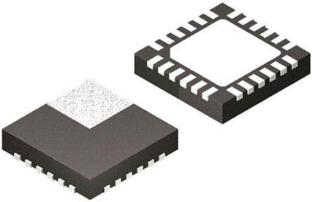
| 产品图片 |
|
| rohs | 符合RoHS无铅 / 符合限制有害物质指令(RoHS)规范要求 |
| 产品系列 | 接口 IC,接口-信号缓冲器、中继器,Texas Instruments SN65LVPE501RGET- |
| 数据手册 | |
| 产品型号 | SN65LVPE501RGET |
| Tx/Rx类型 | * |
| 产品种类 | 接口-信号缓冲器、中继器 |
| 传播延迟时间 | 280 ps |
| 供应商器件封装 | 24-VQFN (4x4) |
| 其它名称 | 296-27572-1 |
| 包装 | 剪切带 (CT) |
| 商标 | Texas Instruments |
| 安装类型 | 表面贴装 |
| 安装风格 | SMD/SMT |
| 封装 | Reel |
| 封装/外壳 | 24-VFQFN 裸露焊盘 |
| 封装/箱体 | VQFN-24 |
| 工作温度 | -40°C ~ 85°C |
| 工作电源电压 | 3 V to 3.6 V |
| 工厂包装数量 | 250 |
| 应用 | PCIe |
| 延迟时间 | 280ps |
| 数据速率(最大值) | 5Gbps |
| 标准包装 | 1 |
| 电压-电源 | 3 V ~ 3.6 V |
| 电容-输入 | - |
| 电流-电源 | 101mA |
| 类型 | 缓冲器, 转接驱动器 |
| 系列 | SN65LVPE501 |
| 输入 | CML |
| 输出 | CML |
| 通道数 | 2 |


PDF Datasheet 数据手册内容提取
SN65LVPE501 www.ti.com SLLSE30A –MAY2010–REVISEDMAY2012 Dual Channel x1 PCIe Redriver/Equalizer CheckforSamples:SN65LVPE501 FEATURES • ExcellentJitterandLossCompensation 1 Capability: • SingleLanePCIeEqualizer/Redriver – 30"of6milStriplineonFR4 • SupportforBothPCIeGenI(2.5Gbps)and GenII(5.0Gbps)Speed • SmallFootPrint–24Pin4 ×4QFNPackage • SelectableEqualization,De-emphasisand • HighProtectionAgainstESDTransient OutputSwingControl – HBM:3,000V • IntegratedTermination – CDM:1,500V • Hot-PlugCapable – MM:200V • ReceiverDetect APPLICATIONS • LowPower: – 330mW(TYP),V =3.3V • PCMB,DockingStations,Backplaneand CC CabledApplication • AutoLowPowerModes: – 5mW(TYP)WhennoConnectionDetected – 70mW(TYP)WheninAuto-LowPower Mode DESCRIPTION The SN65LVPE501 is a dual channel, single lane PCIe redriver and signal conditioner supporting data rates of upto5.0Gbps.ThedevicecomplieswithPCIespecrevision2.1. ProgrammableEQ,De-EmphasisandAmplitudeSwing The SN65LVPE501 is designed to minimize the signal degradation effects such as crosstalk and inter-symbol interference (ISI) that limits the interconnect distance between two devices. The input stage of each channel offers selectable equalization settings that can be programmed to match loss in the channel. The differential outputs provide selectable de-emphasis to compensate for the anticipated distortion PCIe signal will experience. Level of de-emphasis will depend on the length of interconnect and its characteristics. Both equalization and de- emphasislevelsarecontrolledbythesettingofsignalcontrolpinsEQ1,EQ2andDE1,DE2. To provide additional control of signal integrity in extended backplane applications LVPE501 provides independentoutputamplitudecontrolforeachchannel.SeeTable2forsettingdetails. DevicePowerOn Device initiates internal power-on reset after V has stabilized. External reset can also be applied at anytime by CC toggling RST pin. External reset is recommended after every device power-up. When RST is driven high, the devicesamplesthestateofEN_RXD,ifitissetHdeviceentersRx.Detectstatewhereeachchannelwillperform Rx.Detectfunction(asdescribedinPCIespec).IfEN_RXDissetL,automaticRXdetectfunctionisdisabledand bothchannelsareenabledwiththeirterminationsettoZ . DC_RX ReceiverDetection While EN_RXD pin is H and device is not in sleep mode (RST is H), SN65LVPE501 performs RX.Detect on both channels indefinitely until remote termination is detected on both channels. Automatic Rx detection feature can beforcedoffbydrivingEN_RXDlow.InthisstatebothchannelsinputterminationaresettoZ . DC_RX 1 Pleasebeawarethatanimportantnoticeconcerningavailability,standardwarranty,anduseincriticalapplicationsof TexasInstrumentssemiconductorproductsanddisclaimerstheretoappearsattheendofthisdatasheet. PRODUCTIONDATAinformationiscurrentasofpublicationdate. Copyright©2010–2012,TexasInstrumentsIncorporated Products conform to specifications per the terms of the Texas Instruments standard warranty. Production processing does not necessarilyincludetestingofallparameters.
SN65LVPE501 SLLSE30A –MAY2010–REVISEDMAY2012 www.ti.com Thesedeviceshavelimitedbuilt-inESDprotection.Theleadsshouldbeshortedtogetherorthedeviceplacedinconductivefoam duringstorageorhandlingtopreventelectrostaticdamagetotheMOSgates. DESCRIPTION CONTINUED Sleep(Shut_Down)Mode This is low power state triggered by RST = L. In sleep mode receiver termination resistor for each of the two channelsisswitchedtoZ of>50KΩ andtransmittersarepulledtoHi-Zstate.Devicepowerisreduced RX-HIGH_IMP to<1mW(TYP).TogetdeviceoutofsleepmodeRSTistoggledL-H. ElectricalIdleSupport AlinkisinanelectricalidlestatewhentheTX±voltageisheldatasteadyconstantvaluelikethecommonmode voltage. SN65LVPE501 detects an electrical idle state when RX± input voltage of the associated channel falls below V min. After detection of an electrical idle state in a given channel the device asserts electrical idle EID_TH state in its corresponding TX. When RX± voltage exceeds V max, normal device operation is restored and EID_TH outputstartspassinginputsignal.Electricalidleexitandentrytimeisspecifiedat≤6ns. Electricalidlesupportisindependentforeachchannel. PowerSaveFeatures Thedevicesupportsthreepowersavemodesasdescribedbelow. 1. Sleep(Shut_Down)Mode This mode can be enabled from any state (Rx detect or active) by driving RST L. In this state both channels havetheirterminationsettoZ andoutputsareatHi-Z.Devicepoweris1mW(MAX) RX-HIGH_IMP+ 2. AutoLowPowerMode This mode is enabled when PS pin is tied H and device is in active mode. In this mode anytime Vin falls diff_pp below selected V for a given channel and stays below V for >1µs (TYP), the associated CH will EID_TH EID_TH enter auto low power (ALP) mode where power/CH will be reduced to <1/3rd of normal operating power/CH or about 70mW under typical voltage of 3.3V when ALP conditions are met for both channels. A CH will exit ALP mode whenever Vin exceeds max V for that channel. Exit latency is 30ns max. To use this diff_pp EID_TH mode link latency will need to account for the ALP exit time for N_FTS. ALP mode is handled by each channel independently based on its input differential signal level. This mode can be disabled by leaving PS asNCortyingPStoGNDvia4.7kΩ. 3. CableDisconnectMode This mode is activated when RST is H, EN_RXD = H, and no termination is detected by either channel. Device is in the Rx.Detect state whereby it is continuously performing Rx.Detect on both channels. In this statetotalpowerconsumedbydeviceistypically<3%ofnormalactivepower.Or <10mW(MAX). BeaconSupport With its broadband design, the SN65LVPE501 supports low frequency Beacon signal (as defined by PCIe 2.1 spec) used to indicate wake-up event to the system by a downstream device when in L2 power state. All requirements for a beacon signal as specified in PCI Express specification 2.1 must be met for device to pass beaconsignals. DevicPower The SN65LVPE501 is designed to operate from a single 3.3V supply. Always practice proper supply sequencing procedure. Apply V first before any input control pin signals are applied to the device. Power-down sequence CC isinreverseorder. 2 Copyright©2010–2012,TexasInstrumentsIncorporated
SN65LVPE501 www.ti.com SLLSE30A –MAY2010–REVISEDMAY2012 PCIe Instrumentation Chassis compliant /I/O expansion box/ Docking Station cable Server/PC/Notebook Midplane I/O Module R x1 I/O Hub I/O Module x1 R x1 uP I/O Module R ® R SN75LVPE501 Figure1. SN65LVPE501TypicalApplications Copyright©2010–2012,TexasInstrumentsIncorporated 3
SN65LVPE501 SLLSE30A –MAY2010–REVISEDMAY2012 www.ti.com RST Detect RX1+ TX1+ n o ati min Receiver/ CHANNEL1 Driver er Equalizer T al u RX1- D TX1- EQ1 EQ EQ2 CNTRL VBB_TX DE1 DEMP CNTRL DE2 TX2+ n RX2+ o ati n Driver CHANNEL2 Receiver/ mi Equalizer er T al u TX2- D RX2- VBB_TX OS Detect Cntrl. RST OS1 OS2 Figure2. DataFlowBlockDiagram Split System Upstream Board Downstream Board PCIe R RC PCIe Cable EN_RXD CPRSNT# Enclosed System System Board PCIe R RC EN_RXD Mezzanine Card Figure3. TypicalImplementation 4 Copyright©2010–2012,TexasInstrumentsIncorporated
SN65LVPE501 www.ti.com SLLSE30A –MAY2010–REVISEDMAY2012 Table1.PinDescription PIN NUMBER NAME I/OTYPE DESCRIPTION HIGHSPEEDDIFFERENTIALI/OPINS 8 RX1+ I,CML 9 RX1– I,CML Non-invertingandinvertingCMLdifferentialinputforCH1andCH2.Thesepinsaretiedtoan 20 RX2+ I,CML internalvoltagebiasbydualterminationresistorcircuit. 19 RX2– I,CML 23 TX1+ O,CML 22 TX1– O,CML Non-invertingandinvertingCMLdifferentialoutputforCH1andCH2.Thesepinsare 11 TX2+ O,CML internallytiedtovoltagebiasbyterminationresistors. 12 TX2– O,CML DEVICECONTROLPIN(1) 5 EN_RXD I,LVCMOS SetsdeviceoperationmodesperTable2.InternallypulledtoVCC 14 PS I,LVCMOS Selectauto-lowpowersavemodeperTable2.InternallypulledtoGND 7 RST I,LVCMOS Resetdevice,inputactiveLow.InternallypulledtoVCC 24 RSVD I,LVCMOS Reservedforfactorytest.MustbeconnectedtoGND SIGNALCONTROLPINS(2) 3,16 DE1,DE2 I,LVCMOS Selectsde-emphasissettingsforCH1andCH2perTable2.InternallytiedtoV /2 CC 2,17 EQ1,EQ2 I,LVCMOS SelectsequalizationsettingsforCH1andCH2perTable2.InternallytiedtoV /2 CC 4,15 OS1,OS2 I,LVCMOS SelectsoutputamplitudeforCH1andCH2perTable2.InternallytiedtoV /2 CC POWERPINS 1,13 VCC Power Positivesupplyshouldbe3.3V±10% 6,10,18,21 GND Power Supplyground (1) WhennotusedcanbeleftasNCorconnectedtoV /GNDvia4.7kΩresistor. CC (2) InternallybiasedtoV /2with>200kΩpullup/pulldown.When3-statepinsareleftasNCboardleakageatthepinpadmustbe<1µA CC otherwisedrivetoV /2toassertmid-levelstate. CC Copyright©2010–2012,TexasInstrumentsIncorporated 5
SN65LVPE501 SLLSE30A –MAY2010–REVISEDMAY2012 www.ti.com Table2.SignalControlPinSetting TRANSITIONBITAMPLITUDE OSx (TYPmVpp) NC 1000 0 875 1 1100 DEx(1) OSx(1)=NC OSx(1)=0 OSx(1)=1 NC –3.7dB –2.5dB –4.6dB 0 –6.4dB –5.5dB –6.6dB 1 –9.4dB –9.5dB –8.7dB EQx(1) EQUALIZATIONdB (AtGenIISpeed) NC 0 0 7 1 15 EN_RXD DEVICEFUNCTION SetinputterminationtoZ 0 DC_RX anddisableRx.Detect PerformRx.Detect(default, 1 internallypulledtoVcc) RST DEVICEFUNCTION Deviceinquiescentstateand 0 inputssettoHi-Z Devicenotinshut_downmode 1 (default,internallypulledtoVcc) PS DEVICEFUNCTION Auto-lowpowermodedisabled 0 (default,internallypulledtoGND) 1 Auto-lowpowermodeenabled (1) AppliestoChannel1andChannel2at2.5GHz. 6 Copyright©2010–2012,TexasInstrumentsIncorporated
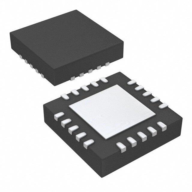
SN65LVPE501 www.ti.com SLLSE30A –MAY2010–REVISEDMAY2012 3.3 V TOPVIEW GND EN_RXD OS1 DE1 EQ1 VCC 6 1 RST 7 SN65LVPE501 24 RSVD 0.1 µF RX1+ TX1+ 0.1 µF CH1 0.1 µF RX1– TX1– 0.1 µF OST GND (muTsth beerm saoll dPearded to GND CE H GND plane) VI E D 0.1 µF TX2+ RX2+ 0.1 µF CH2 0.1 µF TX2– 12 19 RX2– 0.1 µF 13 18 VCC PS OS2 DE2 EQ1 GND 3.3 V (1) This is a reference example and it is not intended to represent the best configuration; every designer should select theEQandDEsettingsthatbetterfitsthesystemneeds.AllDEx,EQxandOSxpinsdefaulttoNC. (2) TherecommendedvalueforalltheresistorsshownintheFigureis4.9KΩ. (3) ForterminalsOSx,DEx,andEQx,populateonlypull-uporonlypull-downaccordingtothedesiredsetting. Figure4. ReferenceDeviceImplementation Copyright©2010–2012,TexasInstrumentsIncorporated 7
SN65LVPE501 SLLSE30A –MAY2010–REVISEDMAY2012 www.ti.com BOTTOM VIEW VCC EQ1 DE1 OS1EN_RXDGND 1 6 SN65LVPE501 RSVD 24 7 RST TX1+ RX1+ CH1 TX1- RX1- Thermal Pad GND (must be soldered to GND GND plane) RX2+ TX2+ CH2 RX2- 19 12 TX2- 18 13 GND EQ2 DE2 OS2 PS VCC TOPVIEW GND EN_RXD OS1 DE1 EQ1 VCC 6 1 SN65LVPE501 RST 7 24 RSVD RX1+ TX1+ CH1 RX1- TX1- Thermal Pad (must be soldered to GND GND GND plane) TX2+ CH2 RX2+ CH2 CH2 TX2- 12 19 RX2- 13 18 VCC PS OS2 DE2 EQ2 GND Figure5. Flow-ThroughPin-Out ORDERINGINFORMATION(1) PARTNUMBER PARTMARKING PCAKAGE SN65LVPE501RGER LVPE501 24-pinRGEReel(large) SN65LVPE501RGET LVPE501 24-pinRGEReel(small) (1) Forthemostcurrentpackageandorderinginformation,seethePackageOptionAddendumattheendofthisdocument,orseetheTI websiteatwww.ti.com. 8 Copyright©2010–2012,TexasInstrumentsIncorporated
SN65LVPE501 www.ti.com SLLSE30A –MAY2010–REVISEDMAY2012 ABSOLUTE MAXIMUM RATINGS overoperatingfree-airtemperaturerange(unlessotherwisenoted)(1) UNIT/VALUES SupplyVoltageRange(2) V –0.5Vto4V CC DifferentialI/O –0.5Vto4V VoltageRange ControlI/O –0.5VtoV +0.5 CC (HumanBodyModel)QSS009-105(JESD22-A114B) ±3000V ElectrostaticDischarge (ChargedDeviceModel)QSS009-147(JESD22-C101-A) ±1500V (MachineModel)JESD22-A115-A ±200V Continuouspowerdissipation SeeThermalInformationTable (1) Stressesbeyondthoselistedunderabsolutemaximumratingsmaycausepermanentdamagetothedevice.Thesearestressratings onlyandfunctionaloperationofthedeviceattheseoranyconditionsbeyondthoseindicatedunderrecommendedoperatingconditions isnotimplied.Exposuretoabsolute-maximum-ratedconditionsforextendedperiodsmayaffectdevicereliability. (2) Allvoltagevalues,exceptdifferentialvoltages,arewithrespecttonetworkgroundterminal. THERMAL INFORMATION SN65LVPE501 THERMALMETRIC(1) RGE UNITS 24PINS θ Junction-to-ambientthermalresistance(2) 46 JA θ Junction-to-case(top)thermalresistance (3) 42 JC(TOP) θ Junction-to-boardthermalresistance (4) 13 JB °C/W ψ Junction-to-topcharacterizationparameter (5) 0.5 JT ψ Junction-to-boardcharacterizationparameter (6) 9 JB θ Junction-to-case(bottom)thermalresistance (7) 4 JC(BOTTOM) (1) Formoreinformationabouttraditionalandnewthermalmetrics,seetheICPackageThermalMetricsapplicationreport,SPRA953. (2) Thejunction-to-ambientthermalresistanceundernaturalconvectionisobtainedinasimulationonaJEDEC-standard,high-Kboard,as specifiedinJESD51-7,inanenvironmentdescribedinJESD51-2a. (3) Thejunction-to-case(top)thermalresistanceisobtainedbysimulatingacoldplatetestonthepackagetop.NospecificJEDEC- standardtestexists,butaclosedescriptioncanbefoundintheANSISEMIstandardG30-88. (4) Thejunction-to-boardthermalresistanceisobtainedbysimulatinginanenvironmentwitharingcoldplatefixturetocontrolthePCB temperature,asdescribedinJESD51-8. (5) Thejunction-to-topcharacterizationparameter,ψ ,estimatesthejunctiontemperatureofadeviceinarealsystemandisextracted JT fromthesimulationdataforobtainingθ ,usingaproceduredescribedinJESD51-2a(sections6and7). JA (6) Thejunction-to-boardcharacterizationparameter,ψ ,estimatesthejunctiontemperatureofadeviceinarealsystemandisextracted JB fromthesimulationdataforobtainingθ ,usingaproceduredescribedinJESD51-2a(sections6and7). JA (7) Thejunction-to-case(bottom)thermalresistanceisobtainedbysimulatingacoldplatetestontheexposed(power)pad.Nospecific JEDECstandardtestexists,butaclosedescriptioncanbefoundintheANSISEMIstandardG30-88. Copyright©2010–2012,TexasInstrumentsIncorporated SubmitDocumentationFeedback 9 ProductFolderLink(s):SN65LVPE501
SN65LVPE501 SLLSE30A –MAY2010–REVISEDMAY2012 www.ti.com RECOMMENDED OPERATING CONDITIONS overoperatingfree-airtemperaturerange(unlessotherwisenoted) MIN TYP MAX UNIT V SupplyVoltage 3 3.3 3.6 V CC C ACCouplingCapacitor 75 200 nF COUPLING Operatingfree-airtemperature –40 85 °C ELECTRICAL CHARACTERISTICS overoperatingfree-airtemperaturerange(unlessotherwisenoted) PARAMETER TESTCONDITIONS MIN TYP MAX UNIT DEVICEPARAMETERS(underrecommendedoperatingconditions,unlessotherwisenoted) RST,DEx,EQx,OSx=NC,EN_RXD=NC,K28.5patternat5Gbps, ICC VID=1000mVp-p 101 120 ICCidle SupplyCurrent PS=1;Whenauto-lowpowerconditionsaremet 21 26 mA ICCshut-down RST=GND 0.2 1 ICCRX.Detect RST,EN_RXD=NC 2 MaximumDataRate 5 Gbps AutoLPENTRY AutoLowPowerEntryTime ElectricalIdleatInput,RefertoFigure9 1.0 1.3 µs AutoLPEXIT AutoLowPowerExitTime Afterfirstsignalactivity,RefertoFigure9 15 30 ns RxDetectStartEvent,Vcc=Stable tPU PowerUpTime RST,EN_RXD=H 15 30 µs Sleep(shut-down)ModeEntry tDIS Time RSTH→L;EN_RXD=X 1 µs TENB Sleep(shut-down)ModeExitTime RSTL→H;EN_RXD=H,StartofExdetectevent 10 µs CONTROLLOGIC(underrecommendedoperatingconditions,unlessotherwisenoted) VIH HighlevelInputVoltage 1.4 VCC V VIL LowLevelInputVoltage –0.3 0.5 V VHYS InputHysteresis 150 mV OSx,EQx,DEx=VCC 30 IIH HighLevelInputCurrent µA EN_RXD,RST=VCC 1 OSx,EQx,DEx=GND –30 IIL LowLevelInputCurrent PS=GND –1 µA EN_RXD,RST=GND –20 RECEIVERAC/DC(underrecommendedoperatingconditions,unlessotherwisenoted) Vindiff_pp RX1,RX2InputVoltageSwing ACcoupleddifferentialsignal 100 1200 mVp-p VCM_RX RX1,RX2CommonModeVoltage 0 3.6 V RX1,RX2ACPeakcommon VinCOM_P modevoltage 150 mVP ZDC_RX DCsingleendedimpedance 40 50 60 Ω Zdiff_RX DCDifferentialInputimpedance 80 100 120 Ω DeviceinsleepmodeRxterminationnotpowered;Measuredwith ZRX_High_IMP+ DCInputHighImpedance respecttoGNDover200mVmax 50 74 kΩ VEID_TH ElectricalIdleDetectThreshold Measuredatreceiverpin(seeFigure7) 65 84 175 mVpp 50MHz–1.25GHz 10 dB RLRX-DIFF DifferentialReturnLoss Operatingtemperature0°Cto85°C 8 1.25GHz–2.5GHz dB Operatingtemperature–40°Cto85°C 7 RLRX-CM CommonModeReturnLoss 50MHz–2.5GHz 10 dB 10 SubmitDocumentationFeedback Copyright©2010–2012,TexasInstrumentsIncorporated ProductFolderLink(s):SN65LVPE501
SN65LVPE501 www.ti.com SLLSE30A –MAY2010–REVISEDMAY2012 ELECTRICAL CHARACTERISTICS (continued) overoperatingfree-airtemperaturerange(unlessotherwisenoted) PARAMETER TESTCONDITIONS MIN TYP MAX UNIT TRANSMITTERAC/DC(underrecommendedoperatingconditions,unlessotherwisenoted) RL=100Ω±1%,DEx,OS=NC,TransitionBit 800 1000 1200 VTXDIFF_PP RL=100Ω±1%,DEx=NC,OSx=GNDTransitionBit 875 mV RL=100Ω±1%,DEx=NC,OSx=VCCTransitionBit 1100 Differentialpeak-to-peakOutput RL=100Ω±1%,DEx=NC,OSx=0,1,NC 655 Voltage Non-TransitionBit VTXDIFF_NTB_PP RNLon=-1T0r0aΩns±iti1o%n,BDitEx=0,OSx=0,1,NC 495 mV RL=100Ω±1%,DEx=1,OSx=0,1, 350 NCNon-TransitionBit DEx,OSx=NC,See Operatingtemperature0°Cto85°C –3.0 –3.7 –4.0 Figure11; dB (forOS1,2=1and0see Operatingtemperature–40°Cto85°C –3.0 –3.7 –4.2 De-EmphasisLevel Table2) DEx=0,OSx=NC –6.4 dB DEx=1,OSx=NC –9.4 TDE De-EmphasisWidth At5Gbps 0.8 UI Zdiff_TX DCDifferentialImpedance Definedduringsignaling 80 100 120 Ω Operatingtemperature0°Cto85°C 10 f=50MHz–1.25GHz. Operatingtemperature–40°Cto85°C 9.5 RLdiff_TX DifferentialReturnLoss dB Operatingtemperature0°Cto85°C 6 f=1.25GHz–2.5GHz, Operatingtemperature–40°Cto85°C 5.5 RLCM_TX CommonModeReturnLoss f=50MHz–2.5GHz 10 dB ITX_SC TXshortcircuitcurrent TX±shortedtoGND 60 90 mA TransmitterDCcommon-mode VTX_CM_DC voltage AllowedDCCMvoltageatTXpins 2.1 2.65 3.1 V TXACcommonmodevoltageat VTX_CM_AC2 GENIIspeed 26 100 mVpp Max(Vd++Vd–)/2–Min(Vd++Vd–)/2 TXACcommonmodevoltageat VTX_CM_AC1 GENIspeed 2 20 mV AbsoluteDeltaDCCMvoltage VTX_CM_DeltaL0-L0s duringactiveandidlestates |VTX_CM_DC[L0]–VTX_CM_DC[L0s]|,PS=L 0 100 mV VDeTltXa_CM-DC-Line- AbebtswoeluetneDD+elatandofDD–CCMvoltage |VTX_CM_DC-D+[L0]–VTX_CM_DC-D-[L0]| 0 25 mV Electricalidledifferentialpeak VTX_idle_diff-AC-p outputvoltage |VTX-Idle-D+–VTX-Idle-D–|HPfilteredtoremoveanyDCcomponent 0 1 10 mVpp DCElectricalidledifferential VTX_idle_diff-DC outputvoltage |VTX_idle-D+–VTX_idle-D–|LPfilteredtoremoveanyACcomponent 3.5 mV Voltagechangetoallowreceiver Vdetect detect Positivevoltagetosensereceiver 600 mV DEx=NC,OS=NC(CH0andCH1)20%-80%ofdifferentialvoltage tR,tF OutputRise/Falltime attheoutput;VID>1000mVpp 30 53 ps DEx=NC,OS=NC(CH0andCH1)20%-80%ofdifferentialvoltage tRF_MM OutputRise/Falltimemismatch attheoutput 1 20 ps DEx=NC(CH0andCH1).Propagationdelaybetween50%levelat Tdiff_LH,Tdiff_HL DifferentialPropagationDelay inputandoutput.SeeFigure6 280 330 ps tidleEntrytidleExit Idleentryandexittimes SeeFigure7 4 6 ns TxEQUALIZATIONatGENIISpeed(underrecommencedoperatingconditions) AtpointAinFigure10(2) 30 50 TTX-TJ(1) TotalJitter AtpointBinFigure10(2) 25 80 pspp AtpointAinFigure10(2) 16 30 TTX-DJ DeterministicJitter AtpointBinFigure10(2) 11 60 pspp (1) IncludesRJat10-12 (2) RefertoFigure10with±K28.5patternat5Gbps,–3.5dBDEfromsourceAWG. Copyright©2010–2012,TexasInstrumentsIncorporated SubmitDocumentationFeedback 11 ProductFolderLink(s):SN65LVPE501
SN65LVPE501 SLLSE30A –MAY2010–REVISEDMAY2012 www.ti.com IN T T diff_LH diff_HL OUT Figure6. PropagationDelay verticalspacer IN+ VEID_TH VCM IN- tidleExit tidleEntry OUT+ V CM OUT- Figure7. IdleModeExitandEntryDelay verticalspacer 80% 20% tr tf Figure8. OutputRiseandFallTimes verticalspacer RX_1,2+ VCM RX RX_1,2- t idleEntry AutoLP EXIT TX_1,2+ VCM TX TX_1,2- AutoLPENTRY Power Saving Mode Figure9. AutoLowPowerModeTiming(whenenabled) 12 SubmitDocumentationFeedback Copyright©2010–2012,TexasInstrumentsIncorporated ProductFolderLink(s):SN65LVPE501
SN65LVPE501 www.ti.com SLLSE30A –MAY2010–REVISEDMAY2012 Jitter Measurement A B 25"6mil 5"6mil Stripline Stripline 1 AWG* 2 B A AWG* A = Device pin + 2" Jitter B = End of trace on test board Measurement Figure10. JitterMeasurementSetup verticalspacer 1-bit 1to N bits 1-bit 1to N bits t DE DEx=NC -3.7dB -6.4dB DEx=0 -9.4dB DEx=1 VTXDIFF_NTB_P-P VTXDIFF_TB_P-P t DE Figure11. OutputDe-EmphasisLevelsOSx=NC Typical Eye Diagram and Performance Curves at Output InputSignalCharacteristics:DataRate=5Gbps,V =1000mVpp,DE=-3.5dB,Pattern=K28.5 ID DeviceOperatingConditions:VCC=3.3V,Temp=25°C DeviceEQsettings(EQ/DE/OS)adjustedforbesteyeperformance Copyright©2010–2012,TexasInstrumentsIncorporated SubmitDocumentationFeedback 13 ProductFolderLink(s):SN65LVPE501
SN65LVPE501 SLLSE30A –MAY2010–REVISEDMAY2012 www.ti.com Output Trace Length Held Constant and Input Trace Length Varied Figure12. InputTrace=4Inches,6mil,andMeasuredatOutputTrace=4Inches verticalspacer Figure13. InputTrace=20Inches,6mil,andMeasuredatOutputTrace=4Inches 14 SubmitDocumentationFeedback Copyright©2010–2012,TexasInstrumentsIncorporated ProductFolderLink(s):SN65LVPE501
SN65LVPE501 www.ti.com SLLSE30A –MAY2010–REVISEDMAY2012 Figure14. InputTrace=32Inches,6mil,andMeasuredatOutputTrace=4Inches verticalspacer Figure15. InputTrace=44Inches,6mil,andMeasuredatOutputTrace=4Inches Copyright©2010–2012,TexasInstrumentsIncorporated SubmitDocumentationFeedback 15 ProductFolderLink(s):SN65LVPE501
SN65LVPE501 SLLSE30A –MAY2010–REVISEDMAY2012 www.ti.com Variable Trace Lengths at Input and Output Figure16. InputTrace=28Inches,6mil,andMeasuredatOutputTrace=24Inches verticalspacer Figure17. InputTrace=44Inches,6mil,andMeasuredatOutputTrace=24Inches 16 SubmitDocumentationFeedback Copyright©2010–2012,TexasInstrumentsIncorporated ProductFolderLink(s):SN65LVPE501
SN65LVPE501 www.ti.com SLLSE30A –MAY2010–REVISEDMAY2012 REVISION HISTORY ChangesfromOriginal(May2010)toRevisionA Page • AddedFigure4 ..................................................................................................................................................................... 7 Copyright©2010–2012,TexasInstrumentsIncorporated SubmitDocumentationFeedback 17 ProductFolderLink(s):SN65LVPE501
PACKAGE OPTION ADDENDUM www.ti.com 6-Feb-2020 PACKAGING INFORMATION Orderable Device Status Package Type Package Pins Package Eco Plan Lead/Ball Finish MSL Peak Temp Op Temp (°C) Device Marking Samples (1) Drawing Qty (2) (6) (3) (4/5) SN65LVPE501RGER ACTIVE VQFN RGE 24 3000 Green (RoHS NIPDAU Level-2-260C-1 YEAR -40 to 85 LVPE501 & no Sb/Br) SN65LVPE501RGET ACTIVE VQFN RGE 24 250 Green (RoHS NIPDAU Level-2-260C-1 YEAR -40 to 85 LVPE501 & no Sb/Br) (1) The marketing status values are defined as follows: ACTIVE: Product device recommended for new designs. LIFEBUY: TI has announced that the device will be discontinued, and a lifetime-buy period is in effect. NRND: Not recommended for new designs. Device is in production to support existing customers, but TI does not recommend using this part in a new design. PREVIEW: Device has been announced but is not in production. Samples may or may not be available. OBSOLETE: TI has discontinued the production of the device. (2) RoHS: TI defines "RoHS" to mean semiconductor products that are compliant with the current EU RoHS requirements for all 10 RoHS substances, including the requirement that RoHS substance do not exceed 0.1% by weight in homogeneous materials. Where designed to be soldered at high temperatures, "RoHS" products are suitable for use in specified lead-free processes. TI may reference these types of products as "Pb-Free". RoHS Exempt: TI defines "RoHS Exempt" to mean products that contain lead but are compliant with EU RoHS pursuant to a specific EU RoHS exemption. Green: TI defines "Green" to mean the content of Chlorine (Cl) and Bromine (Br) based flame retardants meet JS709B low halogen requirements of <=1000ppm threshold. Antimony trioxide based flame retardants must also meet the <=1000ppm threshold requirement. (3) MSL, Peak Temp. - The Moisture Sensitivity Level rating according to the JEDEC industry standard classifications, and peak solder temperature. (4) There may be additional marking, which relates to the logo, the lot trace code information, or the environmental category on the device. (5) Multiple Device Markings will be inside parentheses. Only one Device Marking contained in parentheses and separated by a "~" will appear on a device. If a line is indented then it is a continuation of the previous line and the two combined represent the entire Device Marking for that device. (6) Lead/Ball Finish - Orderable Devices may have multiple material finish options. Finish options are separated by a vertical ruled line. Lead/Ball Finish values may wrap to two lines if the finish value exceeds the maximum column width. Important Information and Disclaimer:The information provided on this page represents TI's knowledge and belief as of the date that it is provided. TI bases its knowledge and belief on information provided by third parties, and makes no representation or warranty as to the accuracy of such information. Efforts are underway to better integrate information from third parties. TI has taken and continues to take reasonable steps to provide representative and accurate information but may not have conducted destructive testing or chemical analysis on incoming materials and chemicals. TI and TI suppliers consider certain information to be proprietary, and thus CAS numbers and other limited information may not be available for release. In no event shall TI's liability arising out of such information exceed the total purchase price of the TI part(s) at issue in this document sold by TI to Customer on an annual basis. Addendum-Page 1
PACKAGE OPTION ADDENDUM www.ti.com 6-Feb-2020 Addendum-Page 2
PACKAGE MATERIALS INFORMATION www.ti.com 22-Jan-2015 TAPE AND REEL INFORMATION *Alldimensionsarenominal Device Package Package Pins SPQ Reel Reel A0 B0 K0 P1 W Pin1 Type Drawing Diameter Width (mm) (mm) (mm) (mm) (mm) Quadrant (mm) W1(mm) SN65LVPE501RGER VQFN RGE 24 3000 330.0 12.4 4.25 4.25 1.15 8.0 12.0 Q2 SN65LVPE501RGET VQFN RGE 24 250 180.0 12.4 4.25 4.25 1.15 8.0 12.0 Q2 PackMaterials-Page1
PACKAGE MATERIALS INFORMATION www.ti.com 22-Jan-2015 *Alldimensionsarenominal Device PackageType PackageDrawing Pins SPQ Length(mm) Width(mm) Height(mm) SN65LVPE501RGER VQFN RGE 24 3000 367.0 367.0 35.0 SN65LVPE501RGET VQFN RGE 24 250 210.0 185.0 35.0 PackMaterials-Page2
GENERIC PACKAGE VIEW RGE 24 VQFN - 1 mm max height PLASTIC QUAD FLATPACK - NO LEAD Images above are just a representation of the package family, actual package may vary. Refer to the product data sheet for package details. 4204104/H
PACKAGE OUTLINE RGE0024C VQFN - 1 mm max height PLASTIC QUAD FLATPACK- NO LEAD A 4.1 B 3.9 4.1 PIN 1 INDEX AREA 3.9 1 MAX C SEATING PLANE 0.05 0.00 2X 2.5 0.08 C 2.1±0.1 (0.2) TYP 7 12 20X 0.5 6 13 2X 25 SYMM 2.5 1 18 0.30 PIN 1 ID 24X 0.18 (OPTIONAL) 24 19 0.1 C A B SYMM 0.50 0.05 C 24X 0.30 4224376 A 072018 NOTES: 1. All linear dimensions are in millimeters. Any dimensions in parenthesis are for reference only. Dimensioning and tolerancing per ASME Y14.5M. 2. This drawing is subject to change without notice. 3. The package thermal pad must be soldered to the printed circuit board for thermal and mechanical performance. www.ti.com
EXAMPLE BOARD LAYOUT RGE0024C VQFN - 1 mm max height PLASTIC QUAD FLATPACK- NO LEAD (3.8) ( 2.1) 24 19 24X (0.6) 24X (0.24) 1 18 20X (0.5) 25 SYMM (3.8) 2X (0.8) (Ø0.2) VIA TYP 6 13 (R0.05) 7 12 2X(0.8) SYMM LAND PATTERN EXAMPLE SCALE: 20X 0.07 MAX 0.07 MIN ALL AROUND METAL ALL AROUND SOLDER MASK OPENING SOLDER MASK METAL UNDER OPENING SOLDER MASK NON SOLDER MASK DEFINED SOLDER MASK (PREFERRED) DEFINED SOLDER MASK DETAILS 4224376 A 072018 NOTES: (continued) 4. This package is designed to be soldered to a thermal pad on the board. For more information, see Texas Instruments literature number SLUA271 (www.ti.comlitslua271) . 5. Solder mask tolerances between and around signal pads can vary based on board fabrication site. www.ti.com
EXAMPLE STENCIL DESIGN RGE0024C VQFN - 1 mm max height PLASTIC QUAD FLATPACK- NO LEAD (0.19) 4X ( 0.94) 24 19 24X (0.58) 24X (0.24) 1 18 20X (0.5) SYMM (3.8) (0.57) TYP 6 13 (R0.05) TYP 25 METAL TYP 7 12 (0.57) TYP SYMM SOLDER PASTE EXAMPLE BASED ON 0.125 mm THICK STENCIL EXPOSED PAD 80 PRINTED COVERAGE BY AREA SCALE: 20X 4224376 A 072018 NOTES: (continued) 6. Laser cutting apertures with trapezoidal walls and rounded corners may offer better paste release. IPC-7525 may have alternate design recommendations.. www.ti.com
IMPORTANTNOTICEANDDISCLAIMER TI PROVIDES TECHNICAL AND RELIABILITY DATA (INCLUDING DATASHEETS), DESIGN RESOURCES (INCLUDING REFERENCE DESIGNS), APPLICATION OR OTHER DESIGN ADVICE, WEB TOOLS, SAFETY INFORMATION, AND OTHER RESOURCES “AS IS” AND WITH ALL FAULTS, AND DISCLAIMS ALL WARRANTIES, EXPRESS AND IMPLIED, INCLUDING WITHOUT LIMITATION ANY IMPLIED WARRANTIES OF MERCHANTABILITY, FITNESS FOR A PARTICULAR PURPOSE OR NON-INFRINGEMENT OF THIRD PARTY INTELLECTUAL PROPERTY RIGHTS. These resources are intended for skilled developers designing with TI products. You are solely responsible for (1) selecting the appropriate TI products for your application, (2) designing, validating and testing your application, and (3) ensuring your application meets applicable standards, and any other safety, security, or other requirements. These resources are subject to change without notice. TI grants you permission to use these resources only for development of an application that uses the TI products described in the resource. Other reproduction and display of these resources is prohibited. No license is granted to any other TI intellectual property right or to any third party intellectual property right. TI disclaims responsibility for, and you will fully indemnify TI and its representatives against, any claims, damages, costs, losses, and liabilities arising out of your use of these resources. TI’s products are provided subject to TI’s Terms of Sale (www.ti.com/legal/termsofsale.html) or other applicable terms available either on ti.com or provided in conjunction with such TI products. TI’s provision of these resources does not expand or otherwise alter TI’s applicable warranties or warranty disclaimers for TI products. Mailing Address: Texas Instruments, Post Office Box 655303, Dallas, Texas 75265 Copyright © 2020, Texas Instruments Incorporated