ICGOO在线商城 > 集成电路(IC) > 接口 - 信号缓冲器,中继器,分配器 > P82B96PW
 Datasheet下载
- 型号: P82B96PW
- 制造商: Texas Instruments
- 库位|库存: xxxx|xxxx
- 要求:
| 数量阶梯 | 香港交货 | 国内含税 |
| +xxxx | $xxxx | ¥xxxx |
查看当月历史价格
查看今年历史价格
P82B96PW产品简介:
ICGOO电子元器件商城为您提供P82B96PW由Texas Instruments设计生产,在icgoo商城现货销售,并且可以通过原厂、代理商等渠道进行代购。 P82B96PW价格参考。Texas InstrumentsP82B96PW封装/规格:接口 - 信号缓冲器,中继器,分配器, Buffer, ReDriver 1 Channel 400kHz 8-TSSOP。您可以下载P82B96PW参考资料、Datasheet数据手册功能说明书,资料中有P82B96PW 详细功能的应用电路图电压和使用方法及教程。
Texas Instruments 的 P82B96PW 是一款信号缓冲器/线路驱动器,属于接口类器件,主要用于增强和扩展数字信号的传输能力。该器件常用于 I²C 总线系统中,作为缓冲器或中继器,以提高总线的负载驱动能力和信号完整性。

其主要应用场景包括:

1. I²C 总线扩展:P82B96PW 可用于扩展 I²C 总线的通信距离,提升总线驱动能力,适用于多从设备连接或长距离布线的场合。

2. 工业自动化系统:在复杂的工业环境中,用于增强信号稳定性,防止因负载过大或噪声干扰导致的通信错误。

3. 通信设备:如网络交换设备、服务器管理系统中,用于提升 I²C 接口的可靠性和驱动能力。

4. 消费类电子产品:在需要多个 I²C 设备连接的嵌入式系统中,用作缓冲隔离,防止总线过载。

5. 汽车电子系统:用于车载控制模块之间的通信接口增强,确保在恶劣电气环境下仍能稳定工作。

该器件支持宽电压范围,具备热插拔保护功能,适合各种需要增强 I²C 信号驱动能力的应用场景。
| 参数 | 数值 |
| 产品目录 | 集成电路 (IC)半导体 |
| 描述 | IC REDRIVER I2C 1CH 8TSSOP缓冲器和线路驱动器 Dual Bidirectional Bus Buffer |
| 产品分类 | |
| 品牌 | Texas Instruments |
| 产品手册 | |
| 产品图片 |
|
| rohs | 符合RoHS无铅 / 符合限制有害物质指令(RoHS)规范要求 |
| 产品系列 | 逻辑集成电路,缓冲器和线路驱动器,Texas Instruments P82B96PW- |
| 数据手册 | |
| 产品型号 | P82B96PW |
| Tx/Rx类型 | I²C 逻辑 |
| 产品种类 | 缓冲器和线路驱动器 |
| 传播延迟时间 | 5 ns |
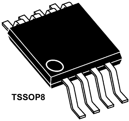
| 供应商器件封装 | 8-TSSOP |
| 其它名称 | 296-33486-5 |
| 包装 | 管件 |
| 单位重量 | 39 mg |
| 商标 | Texas Instruments |
| 安装类型 | 表面贴装 |
| 安装风格 | SMD/SMT |
| 封装 | Tube |
| 封装/外壳 | 8-TSSOP(0.173",4.40mm 宽) |
| 封装/箱体 | TSSOP-8 |
| 工作温度 | -40°C ~ 85°C |
| 工厂包装数量 | 150 |
| 应用 | I²C |
| 延迟时间 | - |
| 数据速率(最大值) | 400kHz |
| 最大工作温度 | + 85 C |
| 最小工作温度 | - 40 C |
| 标准包装 | 150 |
| 电压-电源 | 2 V ~ 15 V |
| 电容-输入 | 4pF |
| 电流-电源 | 4mA |
| 电源电压-最大 | 18 V |
| 电源电压-最小 | - 0.3 V |
| 电源电流 | 0.9 mA |
| 类型 | 缓冲器, 转接驱动器 |
| 系列 | P82B96 |
| 输入 | 2 线式总线 |
| 输出 | 2 线式总线 |
| 通道数 | 1 |
| 逻辑类型 | Bidirectional Bus Buffers |
| 逻辑系列 | P82B96 |


- 商务部:美国ITC正式对集成电路等产品启动337调查
- 曝三星4nm工艺存在良率问题 高通将骁龙8 Gen1或转产台积电
- 太阳诱电将投资9.5亿元在常州建新厂生产MLCC 预计2023年完工
- 英特尔发布欧洲新工厂建设计划 深化IDM 2.0 战略
- 台积电先进制程称霸业界 有大客户加持明年业绩稳了
- 达到5530亿美元!SIA预计今年全球半导体销售额将创下新高
- 英特尔拟将自动驾驶子公司Mobileye上市 估值或超500亿美元
- 三星加码芯片和SET,合并消费电子和移动部门,撤换高东真等 CEO
- 三星电子宣布重大人事变动 还合并消费电子和移动部门
- 海关总署:前11个月进口集成电路产品价值2.52万亿元 增长14.8%


PDF Datasheet 数据手册内容提取
Product Sample & Technical Tools & Support & Folder Buy Documents Software Community P82B96 SCPS144C–MAY2006–REVISEDMAY2015 2 P82B96 I C Compatible Dual Bidirectional Bus Buffer 1 Features 3 Description • OperatingPower-SupplyVoltageRange The P82B96 device is a bus buffer that supports 1 bidirectional data transfer between an I2C bus and a of2Vto15V range of other bus configurations with different • CanInterfaceBetweenI2CBusesOperatingat voltageandcurrentlevels. DifferentLogicLevels(2Vto15V) One of the advantages of the P82B96 is that it • LongerCablesbyallowingbuscapacitanceof supports longer cables/traces and allows for more 400pFonMainSide(Sx/Sy)and4000pFon devices per I2C bus because it can isolate bus TransmissionSide(Tx/Ty) capacitance such that the total loading (devices and • OutputsontheTransmissionSide(Tx/Ty)Have trace lengths) of the new bus or remote I2C nodes HighCurrentSinkCapabilityforDrivingLow- are not apparent to other I2C buses (or nodes). The ImpedanceorHigh-CapacitiveBuses restrictions on the number of I2C devices in a system due to capacitance, or the physical separation • InterfaceWithOptoelectricalIsolatorsandSimilar betweenthem,aregreatlyimproved. DevicesThatNeedUnidirectionalInputand OutputSignalPathsbySplittingI2CBusSignals The device is able to provide galvanic isolation IntoPairsofForward(Tx/Ty)andReverse(Rx/Ry) (optocoupling) or use balanced transmission lines Signals (twisted pairs), because separate directional Tx and Rx signals are provided. The Tx and Rx signals may • 400-kHzFastI2CBusOperationOveratLeast be connected directly (without causing bus latching), 20MetersofWire to provide an bidirectional signal line with I2C • Latch-UpPerformanceExceeds100mAPer properties (open-drain driver). Likewise, the Ty and JESD78,ClassII Rysignalsmayalsobeconnectedtogethertoprovide an bidirectional signal line with I2C properties (open- • ESDProtectionExceedsJESD22 drain driver). This allows for a simple communication design,savingdesigntimeandcosts. 2 Applications • HDMIDDC DeviceInformation(1) • LongI2CCommunication PARTNUMBER PACKAGE BODYSIZE(NOM) • GalvanicI2CIsolation SOIC(8) 4.90mm×3.91mm • IndustrialCommunications VSSOP(8) 3.00mm×3.00mm P82B96 PDIP(8) 9.81mm×6.35mm TSSOP(8) 3.00mm×4.40mm (1) For all available packages, see the orderable addendum at theendofthedatasheet. Long-DistanceI2CCommunications MainEnclosure Remote-ControlEnclosure 12V 12V 3.3–5V 3.3–5V LongCables SCL SCL 3.3–5V 12V 3.3–5V SDA SDA P82B96 P82B96 1 An IMPORTANT NOTICE at the end of this data sheet addresses availability, warranty, changes, use in safety-critical applications, intellectualpropertymattersandotherimportantdisclaimers.PRODUCTIONDATA.
P82B96 SCPS144C–MAY2006–REVISEDMAY2015 www.ti.com Table of Contents 1 Features.................................................................. 1 9 DetailedDescription............................................ 13 2 Applications........................................................... 1 9.1 Overview.................................................................13 3 Description............................................................. 1 9.2 FunctionalBlockDiagram.......................................13 4 RevisionHistory..................................................... 2 9.3 FeatureDescription.................................................14 9.4 DeviceFunctionalModes........................................14 5 Description(continued)......................................... 3 10 ApplicationandImplementation........................ 15 6 PinConfigurationandFunctions......................... 4 10.1 ApplicationInformation..........................................15 7 Specifications......................................................... 5 10.2 TypicalApplications..............................................17 7.1 AbsoluteMaximumRatings .....................................5 11 PowerSupplyRecommendations..................... 21 7.2 ESDRatings..............................................................5 12 Layout................................................................... 21 7.3 RecommendedOperatingConditions.......................5 7.4 ThermalInformation..................................................5 12.1 LayoutGuidelines.................................................21 7.5 ElectricalCharacteristics:V =2.3Vto2.7V........6 12.2 LayoutExample....................................................21 CC 7.6 ElectricalCharacteristics:V =3Vto3.6V...........7 13 DeviceandDocumentationSupport................. 22 CC 7.7 ElectricalCharacteristics:V =4.5Vto5.5V........8 13.1 CommunityResources..........................................22 CC 7.8 ElectricalCharacteristics:V =15V.......................9 13.2 Trademarks...........................................................22 CC 7.9 SwitchingCharacteristics........................................10 13.3 ElectrostaticDischargeCaution............................22 7.10 TypicalCharacteristics..........................................11 13.4 Glossary................................................................22 8 ParameterMeasurementInformation................12 14 Mechanical,Packaging,andOrderable Information........................................................... 22 4 Revision History ChangesfromRevisionB(July2007)toRevisionC Page • AddedPinConfigurationandFunctionssection,ESDRatingstable,FeatureDescriptionsection,DeviceFunctional Modes,ApplicationandImplementationsection,PowerSupplyRecommendationssection,Layoutsection,Device andDocumentationSupportsection,andMechanical,Packaging,andOrderableInformationsection .............................. 1 • ChangedV pinstoVCCpinsinpinoutdiagrams................................................................................................................ 4 CC 2 SubmitDocumentationFeedback Copyright©2006–2015,TexasInstrumentsIncorporated ProductFolderLinks:P82B96
P82B96 www.ti.com SCPS144C–MAY2006–REVISEDMAY2015 5 Description (continued) Two or more Sx or Sy I/Os must not be connected to each other on the same node. The P82B96 design does not support this configuration. Bidirectional I2C signals do not have a direction control pin so, instead, slightly different logic low-voltage levels are used at Sx/Sy to avoid latching of this buffer. A standard I2C low applied at theRx/RyofaP82B96ispropagatedtoSx/Syasabufferedlowwithaslightlyhighervoltagelevel.Ifthisspecial buffered low is applied to the Sx/Sy of another P82B96, the second P82B96 does not recognize it as a standard I2C bus low and does not propagate it to its Tx/Ty output. The Sx/Sy side of P82B96 may not be connected to similarbuffersthatrelyonspeciallogicthresholdsfortheiroperation. The Sx/Sy side of the P82B96 is intended for I2C logic voltage levels of I2C master and slave devices or Tx/Rx signals of a second P82B96, if required. If Rx and Tx are connected, Sx can function as either the SDA or SCL line. Similarly, if Ry and Ty are connected, Sy can function as either the SDA or SCL line. There are no restrictions on the interconnection of the Tx/Rx and Ty/Ry I/O pins to other P82B96s, for example in a star or multi-point configuration (multiple P82B96 devices share the same Tx/Rx and Ty/Ry nodes) with the Tx/Rx and Ty/RyI/Opinsonthecommonbus,andtheSx/Sysideconnectedtotheline-cardslavedevices. In any design, the Sx pins of different devices should never be linked, because the resulting system would be verysusceptibletoinducednoiseandwouldnotsupportallI2Coperatingmodes. Copyright©2006–2015,TexasInstrumentsIncorporated SubmitDocumentationFeedback 3 ProductFolderLinks:P82B96
P82B96 SCPS144C–MAY2006–REVISEDMAY2015 www.ti.com 6 Pin Configuration and Functions PPackage 8-PinPDIP DPackage (TopView) 8-PinSOIC (TopView) Sx 1 8 VCC Sx 1 8 VCC Rx 2 7 Sy Rx 2 7 Sy Tx 3 6 Ry Tx 3 6 Ry GND 4 5 Ty GND 4 5 Ty DGKPackage PWPackage 8-PinVSSOP 8-PinTSSOP (TopView) (TopView) Sx 1 8 VCC Sx 1 8 VCC Rx 2 7 Sy Rx 2 7 Sy Tx 3 6 Ry Tx 3 6 Ry GND 4 5 Ty GND 4 5 Ty PinFunctions PIN I/O DESCRIPTION NO. NAME 1 Sx I/O SerialdatabusorSDA.ConnecttoV ofI2Cmasterthroughapullupresistor. CC 2 Rx I Receivesignal.ConnecttoV ofP82B96throughapullupresistor. CC 3 Tx O Transmitsignal.ConnecttoV ofP82B96throughapullupresistor. CC 4 GND — Ground 5 Ty O Transmitsignal.ConnecttoV ofP82B96throughapullupresistor. CC 6 Ry I Receivesignal.ConnecttoV ofP82B96throughapullupresistor. CC 7 Sy I/O SerialclockbusorSCL.ConnecttoV ofI2Cmasterthroughapullupresistor. CC 8 VCC I Supplyvoltage 4 SubmitDocumentationFeedback Copyright©2006–2015,TexasInstrumentsIncorporated ProductFolderLinks:P82B96
P82B96 www.ti.com SCPS144C–MAY2006–REVISEDMAY2015 7 Specifications 7.1 Absolute Maximum Ratings overoperatingfree-airtemperaturerange(unlessotherwisenoted)(1) MIN MAX UNIT V SupplyvoltageonVCCpin –0.3 18 V CC SxorSy(SDAorSCL) –0.3 18 V Voltageonbufferedinput V I RxorRy –0.3 18 SxorSy(SDAorSCL) –0.3 18 V Voltageonbufferedoutput V O TxorTy –0.3 18 SxorSy 250 I Continuousoutputcurrent mA O TxorTy 250 I ContinuouscurrentthroughVCCorGND 250 mA CC T Operatingfree-airtemperature –40 85 °C A T Storagetemperature –55 125 °C stg (1) StressesbeyondthoselistedunderAbsoluteMaximumRatingsmaycausepermanentdamagetothedevice.Thesearestressratings only,andfunctionaloperationofthedeviceattheseoranyotherconditionsbeyondthoseindicatedunderRecommendedOperating Conditionsisnotimplied.Exposuretoabsolute-maximum-ratedconditionsforextendedperiodsmayaffectdevicereliability. 7.2 ESD Ratings VALUE UNIT HumanBodyModel(HBM),perANSI/ESDA/JEDECJS-001(1) ±3500 Charged-DeviceModel(CDM),perJEDECspecificationJESD22- ±1000 V(ESD) Electrostaticdischarge C101(2) V MachineModel(MM),perJEDECspecificationJESD22-A115-A ±200 (1) JEDECdocumentJEP155statesthat500-VHBMallowssafemanufacturingwithastandardESDcontrolprocess. (2) JEDECdocumentJEP157statesthat250-VCDMallowssafemanufacturingwithastandardESDcontrolprocess. 7.3 Recommended Operating Conditions MIN MAX UNIT V Supplyvoltage 2 15 V CC Sx,Sy V ,V =1V,V ,V ≤0.42V 3 Sx Sy Rx Ry I Low-leveloutputcurrent mA OL Tx,Ty V ,V =0.4V,V ,V =0.4V 30 Sx Sy Tx Ty Sx,Sy V ,V =0.4V 15 Tx Ty V Maximuminput/outputvoltagelevel V IOmax Tx,Ty V ,V =0.4V 15 Sx Sy V Low-levelinputvoltagedifference Sx,Sy 0.4 V ILdiff T Operatingfree-airtemperature –40 85 °C A 7.4 Thermal Information P82B96 THERMALMETRIC(1) D(SOIC) DGK(VSSOP) P(PDIP) PW(TSSOP) UNIT 8PINS 8PINS 8PINS 8PINS R Junction-to-ambientthermalresistance 109.1 174.3 53.5 173.5 °C/W θJA R Junction-to-case(top)thermalresistance 61.6 63 44.4 57.6 °C/W θJC(top) R Junction-to-boardthermalresistance 48.6 94.2 30.6 101.8 °C/W θJB ψ Junction-to-topcharacterizationparameter 19.6 8.1 22.9 5.3 °C/W JT ψ Junction-to-boardcharacterizationparameter 48.2 92.8 30.5 100.2 °C/W JB (1) Formoreinformationabouttraditionalandnewthermalmetrics,seetheSemiconductorandICPackageThermalMetricsapplication report,SPRA953. Copyright©2006–2015,TexasInstrumentsIncorporated SubmitDocumentationFeedback 5 ProductFolderLinks:P82B96
P82B96 SCPS144C–MAY2006–REVISEDMAY2015 www.ti.com 7.5 Electrical Characteristics: V = 2.3 V to 2.7 V CC V =2.3Vto2.7V,voltagesarespecifiedwithrespecttoGND(unlessotherwisenoted) CC TEST TA=25°C TA=–40°Cto85°C PARAMETER UNIT CONDITIONS MIN TYP(1) MAX MIN MAX Temperaturecoefficientof ΔV/ΔT Sx,Sy –2 mV/°C IN inputthresholds I ,I =3mA 0.8 0.88 1 See (2) Sx Sy V Low-leveloutputvoltage Sx,Sy V OL I ,I =0.2mA 0.67 0.73 0.79 See (2) Sx Sy Temperaturecoefficientof ΔV/ΔTOUT outputlowlevels(3) Sx,Sy ISx,ISy=0.2mA –1.8 mV/°C I Quiescentsupplycurrent Sx=Sy=V 0.9 1.8 2 mA CC CC Additionalsupplycurrent ΔI Tx,Ty 1.7 2.75 3 mA CC perpinlow Dynamicoutputsink V ,V >2V, capabilityonI2Cbus VSx,VSy=low 7 18 5.5 mA Rx Ry I Sx,Sy IOS LeakagecurrentonI2Cbus VSx,VSy=2.5V, 0.1 1 1 μA V ,V =high Rx Ry V ,V >1V, Dynamicoutputsink Tx Ty Tx,Ty V ,V =lowon 60 100 60 mA capabilityonbufferedbus I2SCxbuSsy=0.4V I IOT V ,V =V = Leakagecurrent Tx Ty CC 2.5V, 0.1 1 1 μA onbufferedbus V ,V =high Sx Sy InputcurrentfromI2Cbus Sx,Sy Buslow,VRx, –1 1 V =high Ry Inputcurrent Buslow,V , I Rx –1 1 μA I frombufferedbus V =0.4V Ry Rx,Ry Leakagecurrent V ,V =V 1 1.5 onbufferedbusinput Rx Ry CC Inputlogiclevelhigh threshold(4) 0.65 0.7 See (2) onnormalI2Cbus Sx,Sy Inputlogiclevellow threshold(4) 0.6 0.65 See (2) onnormalI2Cbus V Inputthreshold V IT 0.58x 0.58x Inputlogiclevelhigh V V CC CC 0.5x Rx,Ry Inputthreshold V CC 0.42x 0.42x Inputlogiclevellow V V CC CC (V outputlow Sx Input/outputlogiclevel at3mA)– VIOdiff difference(5) Sx,Sy (V inputhighmax) 100 150 100 mV Sx forI2Capplications Sx,Syarelow,V CC V voltageatwhichall Sx,Sy ramping,voltageon V CC 1 1 V IOrel busesarereleased Tx,Ty Tx,Tylowereduntil released Temperaturecoefficientofrelease ΔV/ΔT –4 mV/°C REL voltage C Inputcapacitance Rx,Ry 2.5 4 4 pF in (1) TypicalvalueisatV =2.5V,T =25°C CC A (2) SeetheTypicalCharacteristicssectionofthisdatasheet. (3) Theoutputlogiclowdependsonthesinkcurrent. (4) Theinputlogicthresholdisindependentofthesupplyvoltage. (5) Theminimumvaluerequirementforpullupcurrent,200μA,ensuresthattheminimumvalueforV outputlowalwaysexceedsthe SX minimumV inputhighleveltoeliminateanypossibilityoflatching.Thespecifieddifferenceisspecifiedbydesignwithinanydevice. Sx WhilethetolerancesonabsolutelevelsallowasmallprobabilitythatthelowfromoneSxoutputisrecognizedbyanSxinputofanother P82B96,thishasnoconsequencesfornormalapplications. 6 SubmitDocumentationFeedback Copyright©2006–2015,TexasInstrumentsIncorporated ProductFolderLinks:P82B96
P82B96 www.ti.com SCPS144C–MAY2006–REVISEDMAY2015 7.6 Electrical Characteristics: V = 3 V to 3.6 V CC V =3Vto3.6V,voltagesarespecifiedwithrespecttoGND(unlessotherwisenoted) CC T =25°C T =–40°Cto85°C A A PARAMETER TESTCONDITIONS UNIT MIN TYP(1) MAX MIN MAX Temperature ΔV/ΔT coefficientof Sx,Sy –2 mV/°C IN inputthresholds Low-leveloutput ISx,ISy=3mA 0.8 0.88 1 See (2) V Sx,Sy V OL voltage I ,I =0.2mA 0.67 0.73 0.79 See (2) Sx Sy Temperature coefficientof ΔV/ΔT Sx,Sy I ,I =0.2mA –1.8 mV/°C OUT outputlow Sx Sy levels(3) I Quiescentsupplycurrent Sx=Sy=V 0.9 1.8 2 mA CC CC Additionalsupply ΔI currentperpin Tx,Ty 1.7 2.75 3 mA CC low Dynamicoutput sinkcapability V ,V >2V,V ,V =low 7 18 5.7 mA Sx Sy Rx Ry I onI2Cbus Sx,Sy IOS Leakagecurrent V ,V =5V, onI2Cbus VSx,VSy=high 0.1 1 1 μA Rx Ry Dynamicoutput V ,V >1V, Tx Ty sinkcapability V ,V =lowonI2Cbus= 60 100 60 mA Sx Sy I onbufferedbus Tx,Ty 0.4V IOT Leakagecurrent V ,V =V =3.3V, Tx Ty CC 0.1 1 1 μA onbufferedbus V ,V =high Sx Sy Inputcurrent fromI2Cbus Sx,Sy Buslow,VRx,VRy=high –1 1 Inputcurrent Buslow,V ,V =0.4V –1 1 I frombufferedbus Rx Ry μA I Leakagecurrent Rx,Ry onbufferedbus V ,V =V 1 1.5 Rx Ry CC input Itnhpreusthloogldic(4-)leovnelnhoirgmhalI2Cbus 0.65 0.7 See (2) Sx,Sy Itnhpreusthloogldic(4-)leovnelnloorwmalI2Cbus 0.6 0.65 See (2) V Inputthreshold 0.58x V IT Inputlogiclevelhigh 0.58xV V CC CC Rx,Ry Inputthreshold 0.5xV CC 0.42x 0.42x Inputlogiclevellow V V CC CC (V outputlowat3mA)– VIOdiff Ilenvpeult/doiufftepruetnlcoeg(i5c) Sx,Sy (VSSxxinputhighmax)forI2C 100 150 100 mV applications V voltageat Sx,Syarelow,V ramping, CC Sx,Sy CC V whichallbuses voltageonTx,Tylowereduntil 1 1 V IOrel Tx,Ty arereleased released Temperaturecoefficientof ΔV/ΔT –4 mV/°C REL releasevoltage C Inputcapacitance Rx,Ry 2.5 4 4 pF in (1) TypicalvalueisatV =3.3V,T =25°C CC A (2) SeetheTypicalCharacteristicssectionofthisdatasheet. (3) Theoutputlogiclowdependsonthesinkcurrent. (4) Theinputlogicthresholdisindependentofthesupplyvoltage. (5) Theminimumvaluerequirementforpullupcurrent,200μA,ensuresthattheminimumvalueforV outputlowalwaysexceedsthe SX minimumV inputhighleveltoeliminateanypossibilityoflatching.Thespecifieddifferenceisspecifiedbydesignwithinanydevice. Sx WhilethetolerancesonabsolutelevelsallowasmallprobabilitythatthelowfromoneSxoutputisrecognizedbyanSxinputofanother P82B96,thishasnoconsequencesfornormalapplications. Copyright©2006–2015,TexasInstrumentsIncorporated SubmitDocumentationFeedback 7 ProductFolderLinks:P82B96
P82B96 SCPS144C–MAY2006–REVISEDMAY2015 www.ti.com 7.7 Electrical Characteristics: V = 4.5 V to 5.5 V CC V =4.5Vto5.5V,voltagesarespecifiedwithrespecttoGND(unlessotherwisenoted) CC T =25°C T =–40°Cto85°C A A PARAMETER TESTCONDITIONS UNIT MIN TYP(1) MAX MIN MAX Temperature ΔV/ΔT coefficientofinput Sx,Sy –2 mV/°C IN thresholds Low-leveloutput ISx,ISy=3mA 0.8 0.88 1 See (2) V Sx,Sy V OL voltage I ,I =0.2mA 0.67 0.73 0.79 See (2) Sx Sy Temperature coefficientof ΔV/ΔT Sx,Sy I ,I =0.2mA –1.8 mV/°C OUT outputlow Sx Sy levels(3) I Quiescentsupplycurrent Sx=Sy=V 0.9 1.8 2 mA CC CC Additionalsupply ΔI current Tx,Ty 1.7 2.75 3 mA CC perpinlow Dynamicoutput V ,V >2V, sinkcapability Sx Sy 7 18 6 mA I onI2Cbus Sx,Sy VRx,VRy=low IOS Leakagecurrent V ,V =5V, onI2Cbus VSx,VSy=high 0.1 1 1 μA Rx Ry Dynamicoutput V ,V >1V, Tx Ty sinkcapability V ,V =lowonI2Cbus= 60 100 60 mA Sx Sy I onbufferedbus Tx,Ty 0.4V IOT Leakagecurrent V ,V =V =5V, Tx Ty CC 0.1 1 1 μA onbufferedbus V ,V =high Sx Sy Inputcurrent fromI2Cbus Sx,Sy Buslow,VRx,VRy=high –1 1 Inputcurrent Buslow,V ,V =0.4V –1 1 I frombufferedbus Rx Ry μA I Leakagecurrent Rx,Ry onbufferedbus V ,V =V 1 1.5 Rx Ry CC input Inputlogic-levelhigh threshold(4) 0.65 0.7 See (2) onnormalI2Cbus Sx,Sy Inputlogic-levellow threshold(4) 0.6 0.65 See (2) onnormalI2Cbus V Inputthreshold V IT 0.58x Inputlogiclevelhigh 0.58xV V CC CC Rx,Ry Inputthreshold 0.5xV CC 0.42x 0.42x Inputlogiclevellow V V CC CC (V outputlowat3mA)– VIOdiff Ilenvpeult/doiufftepruetnlcoeg(i5c) Sx,Sy (VSSxxinputhighmax)forI2C 100 150 100 mV applications V voltageat Sx,Syarelow,V CC Sx,Sy CC V whichallbuses ramping,voltageonTx,Ty 1 1 V IOrel Tx,Ty arereleased lowereduntilreleased (1) TypicalvalueisatV =5V,T =25°C CC A (2) SeetheTypicalCharacteristicssectionofthisdatasheet. (3) Theoutputlogiclowdependsonthesinkcurrent. (4) Theinputlogicthresholdisindependentofthesupplyvoltage. (5) Theminimumvaluerequirementforpullupcurrent,200μA,ensuresthattheminimumvalueforV outputlowalwaysexceedsthe SX minimumV inputhighleveltoeliminateanypossibilityoflatching.Thespecifieddifferenceisspecifiedbydesignwithinanydevice. Sx WhilethetolerancesonabsolutelevelsallowasmallprobabilitythatthelowfromoneSxoutputisrecognizedbyanSxinputofanother P82B96,thishasnoconsequencesfornormalapplications. 8 SubmitDocumentationFeedback Copyright©2006–2015,TexasInstrumentsIncorporated ProductFolderLinks:P82B96
P82B96 www.ti.com SCPS144C–MAY2006–REVISEDMAY2015 Electrical Characteristics: V = 4.5 V to 5.5 V (continued) CC V =4.5Vto5.5V,voltagesarespecifiedwithrespecttoGND(unlessotherwisenoted) CC T =25°C T =–40°Cto85°C A A PARAMETER TESTCONDITIONS UNIT MIN TYP(1) MAX MIN MAX Temperaturecoefficientof ΔV/ΔT –4 mV/°C REL releasevoltage C Inputcapacitance Rx,Ry 2.5 4 4 pF in 7.8 Electrical Characteristics: V = 15 V CC V =15V,voltagesarespecifiedwithrespecttoGND(unlessotherwisenoted) CC T =25°C T =–40°Cto85°C A A PARAMETER TESTCONDITIONS UNIT MIN TYP(1) MAX MIN MAX Temperature ΔV/ΔT coefficientof Sx,Sy –2 mV/°C IN inputthresholds Low-leveloutput ISx,ISy=3mA 0.8 0.88 1 See (2) V Sx,Sy V OL voltage I ,I =0.2mA 0.67 0.73 0.79 See (2) Sx Sy Temperature coefficientof ΔV/ΔT Sx,Sy I ,I =0.2mA –1.8 mV/°C OUT outputlow Sx Sy levels(3) Quiescentsupply I Sx=Sy=V 0.9 1.8 2 mA CC current CC Additionalsupply ΔI current Tx,Ty 1.7 2.75 3 mA CC perpinlow Dynamicoutput V ,V >2V, sinkcapability Sx Sy 7 18 6.5 mA I onI2Cbus Sx,Sy VRx,VRy=low IOS Leakagecurrent V ,V =15V, onI2Cbus VSx,VSy=high 0.1 1 1 μA Rx Ry Dynamicoutput V ,V >1V, Tx Ty sinkcapability V ,V =lowonI2Cbus 60 100 60 mA Sx Sy I onbufferedbus Tx,Ty =0.4V IOT Leakagecurrent V ,V =V =15V, Tx Ty CC 0.1 1 1 μA onbufferedbus V ,V =high Sx Sy Inputcurrent fromI2Cbus Sx,Sy Buslow,VRx,VRy=high –1 1 Inputcurrent Buslow,V ,V =0.4V –1 1 I frombufferedbus Rx Ry μA I Leakagecurrent Rx,Ry onbufferedbus V ,V =V 1 1.5 Rx Ry CC input Inputlogic-levelhigh threshold(4) 0.65 0.7 See (2) onnormalI2Cbus Sx,Sy Inputlogic-levelhigh threshold(4) 0.6 0.65 See (2) onnormalI2Cbus V Inputthreshold V IT 0.58x Inputlogiclevelhigh 0.58xV V CC CC Rx,Ry Inputthreshold 0.5xV CC 0.42x 0.42x Inputlogiclevellow V V CC CC (1) TypicalvalueisatV =15V,T =25°C CC A (2) SeetheTypicalCharacteristicssectionofthisdatasheet. (3) Theoutputlogiclowdependsonthesinkcurrent. (4) Theinputlogicthresholdisindependentofthesupplyvoltage. Copyright©2006–2015,TexasInstrumentsIncorporated SubmitDocumentationFeedback 9 ProductFolderLinks:P82B96
P82B96 SCPS144C–MAY2006–REVISEDMAY2015 www.ti.com Electrical Characteristics: V = 15 V (continued) CC V =15V,voltagesarespecifiedwithrespecttoGND(unlessotherwisenoted) CC T =25°C T =–40°Cto85°C A A PARAMETER TESTCONDITIONS UNIT MIN TYP(1) MAX MIN MAX (V outputlowat3mA)– Input/outputlogic Sx VIOdiff leveldifference(5) Sx,Sy (I2VCSxaipnppluictahtiiognhsmax)for 100 150 100 mV V voltageat Sx,Syarelow,V CC Sx,Sy CC V whichallbuses ramping,voltageonTx, 1 1 V IOrel Tx,Ty arereleased Tylowereduntilreleased Temperaturecoefficientof ΔV/ΔT –4 mV/°C REL releasevoltage C Inputcapacitance Rx,Ry 2.5 4 4 pF in (5) Theminimumvaluerequirementforpullupcurrent,200μA,ensuresthattheminimumvalueforV outputlowalwaysexceedsthe SX minimumV inputhighleveltoeliminateanypossibilityoflatching.Thespecifieddifferenceisspecifiedbydesignwithinanydevice. Sx WhilethetolerancesonabsolutelevelsallowasmallprobabilitythatthelowfromoneSxoutputisrecognizedbyanSxinputofanother P82B96,thishasnoconsequencesfornormalapplications. 7.9 Switching Characteristics V =5V,T =25°C,nocapacitiveloads,voltagesarespecifiedwithrespecttoGND(unlessotherwisenoted) CC A FROM TO PARAMETER TESTCONDITIONS TYP UNIT (INPUT) (OUTPUT) R pullup=160Ω, Bufferdelaytimeonfalling V (orV )=inputswitching V (orV )outputfalling Tx tpzl input thSrxesholdSy 50T%x ofVTy (1) CTx=7pF+board 70 ns LOAD tracecapacitance R pullup=160Ω, Bufferdelaytimeonrising V (orV )=inputswitching V (orV )output Tx tplz input thSrxesholdSy reTaxchingT5y0%ofV (2) CTx=7pF+board 90 ns LOAD tracecapacitance R pullup=1500Ω, Bufferdelaytimeonfalling V (orV )=inputswitching V (orV )outputfalling Sx tpzl input thRrexsholdRy 50S%x ofVSy (3) CTx=7pF+board 250 ns LOAD tracecapacitance R pullup=1500Ω, Bufferdelaytimeonrising V (orV )=inputswitching V (orV )output Sx tplz input thRrexsholdRy reSaxchingS5y0%ofV (4) CTx=7pF+board 270 ns LOAD tracecapacitance (1) ThefalltimeofV from5Vto2.5Vinthetestisapproximately15ns. Tx (2) TherisetimeofV from0Vto2.5Vinthetestisapproximately20ns. Tx (3) ThefalltimeofV from5Vto2.5Vinthetestisapproximately50ns. Sx (4) TherisetimeofV from0.9Vto2.5Vinthetestisapproximately70ns. Sx 10 SubmitDocumentationFeedback Copyright©2006–2015,TexasInstrumentsIncorporated ProductFolderLinks:P82B96
P82B96 www.ti.com SCPS144C–MAY2006–REVISEDMAY2015 7.10 Typical Characteristics 1000 1200 Maximum Maximum 1000 mV 800 Typical mV Typical – – 800 VOL 600 VOL Minimum Minimum 600 400 400 -50 –25 0 25 50 75 100125 -50 –25 0 25 50 75 100125 Tj– °C Tj– °C Figure1.VOLatSxvsJunctionTemperature,IOL=0.2mA Figure2.VOLatSxvsJunctionTemperature,IOL=3mA 1000 1000 800 800 V V m m – 600 – 600 VIL(max) 400 VIH(min) 400 200 200 -50 –25 0 25 50 75 100125 -50 –25 0 25 50 75 100125 Tj– °C Tj– °C Figure3.VIL(max)atSxvsJunctionTemperature Figure4.VIH(min)atSxvsJunctionTemperature 1400 1200 V m – 1000 VCC(max) 800 600 400 -50 –25 0 25 50 75 100125 T – °C j Figure5.V vsJunctionTemperature CC(max) Copyright©2006–2015,TexasInstrumentsIncorporated SubmitDocumentationFeedback 11 ProductFolderLinks:P82B96
P82B96 SCPS144C–MAY2006–REVISEDMAY2015 www.ti.com 8 Parameter Measurement Information VCC VCC VIN VOUT R = 160 to 1500W S1 PULSE L DUT GENERATOR GND C = Probe and jig capacitance RT (sLee Note A) TEST S1 tPLZ/tPZL VCC TEST CIRCUIT FOR OPEN-DRAIN OUTPUT V CC Sx or Sy 0.6V 0V t t PZL PLZ V CC Tx orTy 0.5´V CC V OL VOLTAGEWAVEFORMS PROPAGATION DELAY AND OUTPUTTRANSITIONTIMES A. C includesprobeandjigcapacitance. L B. Allinputsaresuppliedbygeneratorshavingthefollowingcharacteristics:PRR≤10MHz,Z =50Ω,t/t ≤30ns. O r f Figure6. TestCircuitandVoltageWaveforms 12 SubmitDocumentationFeedback Copyright©2006–2015,TexasInstrumentsIncorporated ProductFolderLinks:P82B96
P82B96 www.ti.com SCPS144C–MAY2006–REVISEDMAY2015 9 Detailed Description 9.1 Overview TheP82B96isabusbufferthatsupportsbidirectionaldatatransferbetweenanI2Cbusandarangeofotherbus configurationswithdifferentvoltageandcurrentlevels. OneoftheadvantagesoftheP82B96isthatitsupportslongercables/tracesandallowsformoredevicesperI2C bus because it can isolate bus capacitance such that the total loading (devices and trace lengths) of the new bus or remote I2C nodes are not apparent to other I2C buses (or nodes). The restrictions on the number of I2C devicesinasystemduetocapacitance,orthephysicalseparationbetweenthem,aregreatlyimproved. The P82B96 is able to provide galvanic isolation (optocoupling) or use balanced transmission lines (twisted pairs), because separate directional Tx and Rx signals are provided. The Tx and Rx signals may be connected directly (without causing bus latching), to provide an bidirectional signal line with I2C properties (open-drain driver). Likewise, the Ty and Ry signals may also be connected together to provide an bidirectional signal line with I2C properties (open-drain driver). This allows for a simple communication design, saving design time and costs. Two or more Sx or Sy I/Os must not be connected to each other on the same node. The P82B96 design does not support this configuration. Bidirectional I2C signals do not have a direction control pin so, instead, slightly different logic low-voltage levels are used at Sx/Sy to avoid latching of this buffer. A standard I2C low applied at theRx/RyofaP82B96ispropagatedtoSx/Syasabufferedlowwithaslightlyhighervoltagelevel.Ifthisspecial buffered low is applied to the Sx/Sy of another P82B96, the second P82B96 does not recognize it as a standard I2C bus low and does not propagate it to its Tx/Ty output. The Sx/Sy side of P82B96 may not be connected to similarbuffersthatrelyonspeciallogicthresholdsfortheiroperation. The Sx/Sy side of the P82B96 is intended for I2C logic voltage levels of I2C master and slave devices or Tx/Rx signals of a second P82B96, if required. If Rx and Tx are connected, Sx can function as either the SDA or SCL line. Similarly, if Ry and Ty are connected, Sy can function as either the SDA or SCL line. There are no restrictions on the interconnection of the Tx/Rx and Ty/Ry I/O pins to other P82B96s, for example in a star or multi-point configuration (multiple P82B96 devices share the same Tx/Rx and Ty/Ry nodes) with the Tx/Rx and Ty/RyI/Opinsonthecommonbus,andtheSx/Sysideconnectedtotheline-cardslavedevices. In any design, the Sx pins of different devices should never be linked, because the resulting system would be verysusceptibletoinducednoiseandwouldnotsupportallI2Coperatingmodes. 9.2 Functional Block Diagram VCC (2–15 V) 8 Sx(SDA) 1 3 Tx(TxD,SDA) 2 Rx(RxD,SDA) 7 5 Sy(SCL) Ty(TxD,SCL) 6 Ry(RxD,SCL) P82B96 4 GND Copyright©2006–2015,TexasInstrumentsIncorporated SubmitDocumentationFeedback 13 ProductFolderLinks:P82B96
P82B96 SCPS144C–MAY2006–REVISEDMAY2015 www.ti.com 9.3 Feature Description 9.3.1 SxandSy The I2C pins, Sx and Sy, are designed to interface directly with an I2C bus. The logic threshold-voltage levels on the I2C bus are independent of the supply V . The maximum I2C bus supply voltage is 15 V, and the specified CC staticsinkcurrentis3mA. Sx and Sy have two identical buffers. Each buffer is made up of two logic signal paths. The first one, named Tx or Ty, is a forward path from the I2C interface pin, which drives the buffered bus. The second one, named Rx or Ry,isareversesignalpathfromthebufferedbusinputtodrivetheI2Cbusinterface. There are two purposes for these paths: to sense the voltage state of the I2C pin (Sx or Sy) and transmit this state to Tx or Ty, respectively, and to detect the state of the Rx or Ry and pull the I2C pin low when Rx or Ry is low. 9.3.2 TxandTy Tx and Ty are open-collector outputs without ESD protection diodes to V . Each pin may be connected through CC apullupresistortoasupplyvoltageinexcessofV ,aslongasthe15-Vratingisnotexceeded.TxandTyhave CC a larger current-sinking capability than a standard I2C device and can sink a static current of greater than 30 mA. Theyalsohavedynamicpulldowncapabilityof100-mA,typically. A logic low is transmitted to Tx or Ty only when the voltage at the I2C pin (Sx or Sy) is less than 0.6 V. A logic low at Rx or Ry causes the I2C bus (Sx or Sy) to be pulled to a logic low level in accordance with I2C requirements (maximum 1.5 V in 5-V applications), but not low enough to be looped back to the Tx or Ty output andcausethebuffertolatchlow. TheminimumlowlevelthattheP82B96canachieveontheI2CbusbyalowatRxorRytypicallyis0.8V. If V fails, neither the I2C pins nor the Tx or Ty outputs are held low. Their open-collector configuration allows CC them to be pulled up to the rated maximum of 15 V without V present. The input configuration on Sx, Sy, Rx, CC and Ry also presents no loading of external signals when V is not present. This ensures that communication CC onthemainI2CbuscancontinueiftheP82B96hasnosupply. The effective input capacitance of any signal pin, measured by its effect on bus rise times, is less than 4 pF for allbusvoltagesandsupplyvoltages,includingV =0V. CC 9.3.3 LongCableLength The P82B96 supports 400 pF on the main I2C bus (Sx/Sy side) and up to 4000 pF on the transmission side (Tx/Ty). This allows for longer cables to be used due to the significant increase in capacitance allowed by the device. 9.4 Device Functional Modes The P82B96 begins functioning once V reaches 2 V. When V is low, the P82B96 does not hold the Sx/Sy CC CC pinslow,whichensuresI2CcommunicationcancontinuebetweenotherdevicesonthebuswhiletheV islow. CC 14 SubmitDocumentationFeedback Copyright©2006–2015,TexasInstrumentsIncorporated ProductFolderLinks:P82B96
P82B96 www.ti.com SCPS144C–MAY2006–REVISEDMAY2015 10 Application and Implementation NOTE Information in the following applications sections is not part of the TI component specification, and TI does not warrant its accuracy or completeness. TI’s customers are responsible for determining suitability of components for their purposes. Customers should validateandtesttheirdesignimplementationtoconfirmsystemfunctionality. 10.1 Application Information 10.1.1 CalculatingSystemDelaysandBus-ClockFrequencyforFastModeSystem Figure 7 through Figure 9 show the P82B96 used to drive extended bus wiring, with relatively large capacitance (up to 4000 pF), linking two Fast mode I2C bus nodes. It includes simplified expressions for making the relevant timing calculations for 3.3-/5-V operation. It may be necessary to decrease the nominal SCL frequency below 400 kHz, because the buffers and the wiring introduce timing delays. In most cases, the actual bus frequency is lowerthanthenominalmastertiming,duetobit-wisestretchingoftheclockperiods. LocalMasterBus Buffered Expansion Bus Remote Slave Bus VCCM VCCB VCCS Rm Rb Rs SCL SCL MASTER SLAVE Sx Tx/Rx Tx/Rx Sx P82B96 P82B96 I2C I2C Cm = Master Bus Cb = Buffered Bus Cs = Slave Bus Capacitance Wiring Capacitance Capacitance GND FallingedgeofSCLatmasterisdelayedbythebuffersandbusfalltimes. Effective Delay of SCLat Slave = 255 + 17 V + (2.5 + 4×10⁹Cb) V (ns) CCM CCB C = F, V = Volts Figure7. LinkingTwoI2CBusNodesOveraLongCable,MastertoSlave Local Master Bus Buffered Expansion Bus V V CCM CCB Rm Rb SCL MASTER Sx Tx/Rx P82B96 Tx/Rx I2C Cm = Master Bus Cb = Buffered Bus Capacitance Wiring Capacitance GND Rising edge of SCLat master is delayed (clock stretch) by buffer and bus rise times. Effective delay of SCLat master = 270 + RmCm + 0.7RbCb (ns) C = F, R =Ω Figure8. MasterI2CNodeConnectiontoP82B96 Copyright©2006–2015,TexasInstrumentsIncorporated SubmitDocumentationFeedback 15 ProductFolderLinks:P82B96
P82B96 SCPS144C–MAY2006–REVISEDMAY2015 www.ti.com Application Information (continued) LocalMasterBus Buffered Expansion Bus Remote Slave Bus VCCM VCCB VCCS MASTER SDA Rm Rb Rs SDA SLAVE Sx P82B96 Tx/Rx Tx/Rx P82B96 Sx I2C I2C Cm = Master Bus Cb = Buffered Bus Cs = Slave Bus Capacitance Wiring Capacitance Capacitance GND Rising edge of SDAat slave is delayed by the buffers and bus rise times. Effective delay of SDAat master = 270 + 0.2RsCs + 0.7(RbCb + RmCm) (ns) C = F, R =Ω Figure9. LinkingTwoI2CBusNodesOveraLongCable,SlavetoMaster Thedelayfactorsinvolvedincalculationoftheallowedbusspeedare: • The propagation delay of the master signal through the buffers and wiring to the slave. The important delay is thatofthefallingedgeofSCL,becausethisedgerequeststhedataorACKfromaslave. • The effective stretching of the nominal low period of SCL at the master, caused by the buffer and bus rise times. • The propagation delay of the slave response signal through the buffers and wiring back to the master. The important delay is that of a rising edge in the SDA signal. Rising edges always are slower and, therefore, are delayed by a longer time than falling edges. (The rising edges are limited by the passive pullup, while falling edgesactivelyaredriven.) The timing requirement in any I2C system is that a slave’s data response (which is provided in response to a falling edge of SCL) must be received at the master before the end of the corresponding low period of SCL as it appears on the bus wiring at the master. Because all slaves, as a minimum, satisfy the worst-case timing requirements of a 400-kHz part, they must provide their response within the minimum allowed clock low period of 1300ns.Therefore,insystemsthatintroduceadditionaldelays,itisnecessaryonlytoextendthatminimumclock low period by any effective delay of the slave response. The effective delay of the slave's response equals the total delays in SCL falling edge from the master reaching the slave (A) minus the effective delay (stretch) of the SCLrisingedge(B)plustotaldelaysintheslaveresponsedata,carriedonSDA,andreachingthemaster(C). The master microcontroller should be programmed to produce a nominal SCL low period of (1300 + A – B + C) ns and should be programmed to produce the nominal minimum SCL high period of 600 ns. Then, a check should be made to ensure the cycle time is not shorter than the minimum 2500 ns. If foundtobenecessary,increaseeitherclockperiod. Duetoclockstretching,theSCLcycletimealwaysislongerthan(600+1300+A+C)ns. 10.1.1.1 SampleCalculations ThemasterbushasanRmCmproductof100nsandV =5V. CCM The buffered bus has a capacitance of 1 nF and a pullup resistor of 160 Ω to 5 V, giving an RbCb product of 160ns.TheslavebusalsohasanRsCsproductof100ns. The master low period should be programmed to be ≥(1300 + 372.5 – 482 + 472) ns, which calculates to ≥1662.5ns. The master high period may be programmed to the minimum 600 ns. The nominal master clock period is ≥(1662.5+600)ns=2262.5ns,equivalenttoafrequencyof442kHz. The actual bus-clock period, including the 482-ns clock stretch effect, is below (nominal+stretch)=(2262.5+482)nsor≥2745ns,equivalenttoanallowablefrequencyof364kHz. 16 SubmitDocumentationFeedback Copyright©2006–2015,TexasInstrumentsIncorporated ProductFolderLinks:P82B96
P82B96 www.ti.com SCPS144C–MAY2006–REVISEDMAY2015 10.2 Typical Applications 10.2.1 DrivingRibbonorFlatTelephoneCables +VCableDrive V V CC1 CC2 R2 R2 R2 R2 VCC R1 R1 R1 R1 VCC Rx Rx SCL Sx Tx Tx Sx SCL Ty Ty I2C I2C SLAVE(S) MASTER SDA Sy Ry Ry Sy SDA Cable P82B96 P82B96 C2 C2 Propagation Delay = 5 ns/m C2 C2 GND GND BAT54A BAT54A Figure10. DrivingRibbonorFlatTelephoneCables 10.2.1.1 DesignRequirements Inthisapplication,theP82B96isusedtodrivearibboncable.Thefollowingareassumedtobetrue • Sy/SxsideofI2Cbusisataknownvoltagefrom3.3Vto5V • Tx/TyandRx/RysideofI2Cbusisataknownvoltagefrom2Vto15V • SCLClockSpeed<=400kHz 10.2.1.2 DetailedDesignProcedure Table1.BusCapabilities MASTERSCL +V CABLE CABLE PULSE BUS MAXIMUM VCC1 CABLE VCC2 R1 R2 C2 LENGTH CABLE DELAY DURATION CLOCK SLAVE (V) (V) (V) (Ω) (kΩ) (pF) (m) CAPACITANCE (ns) (ns) SPEED RESPONSE (kHz) DELAY HIGH LOW 5 12 5 750 2.2 400 250 (1) 1250 600 4000 120 (2) 5 12 5 750 2.2 220 100 (1) 500 600 2600 185 (2) 3.3 5 3.3 330 1 220 25 1nF 125 600 1500 390 (2) 3.3 5 3.3 330 1 100 3 120pF 15 600 1000 500 600ns (1) Notapplicable;calculationsaredelaybased. (2) Normal400-kHzbusspecification When the master SCL high and low periods can be programmed separately, the timings can allow for bus delays. The low period should be programmed to achieve the minimum 1300 ns plus the net delay in the slave response data signal caused by bus and buffer delays. The longest data delay is the sum of the delay of the falling edge of SCL from master to slave and the delay of the rising edge of SDA from slave data to master. The actual SCL frequency is lower than calculated from the programmed clock periods because the buffer stretches the programmed SCL low period. In the example for the 25-m cable in Table 1, the clock is stretched 400 ns, the falling edge of SCL is delayed 490 ns, and the SDA rising edge is delayed 570 ns. The required additional low period is (490 + 570) = 1060 ns and the I2C bus specifications already include an allowance for a worst-case bus rise time (0% to 70%) of 425 ns. The bus rise time can be 300 ns (30% to 70%), which means it can be 425 ns (0% to 70%). The 25-m cable delay times include all rise and fall times. Therefore, the device only needs to be programmed with an additional (1060 – 400 – 425) = 235 ns, making a total programmed low period 1535 ns. The programmed low is stretched by 400 ns to yield an actual bus low time of 1935 ns, which, allowing the minimumhighperiodof600ns,yieldsacycleperiodof2535nsor394kHz. Copyright©2006–2015,TexasInstrumentsIncorporated SubmitDocumentationFeedback 17 ProductFolderLinks:P82B96
P82B96 SCPS144C–MAY2006–REVISEDMAY2015 www.ti.com Note in both the 100-m and 250-m examples, the capacitive loading on the I2C buses at each end is within the maximum allowed Standard mode loading of 400 pF, but exceeds the Fast mode limit. This is an example of a hybrid mode, because it relies on the response delays of Fast mode parts, but uses (allowable) Standard mode bus loadings with rise times that contribute significantly to the system delays. The cables cause large propagation delays. Therefore, these systems must operate well below the 400-kHz limit, but illustrate how they still can exceed the 100-kHz limit, provided all parts are capable of Fast mode operation. The fastest example illustrates how the 400-kHz limit can be exceeded, provided master and slave parts have delay specifications smaller than the maximum allowed. Many TI slaves have delays shorter than 600 ns, but none have that specified. 10.2.1.3 ApplicationCurve 6 Input Output 5 4 V) e ( ud 3 plit m A 2 1 0 D001 Figure11. PropagationDelayThroughP82B96With400-KHzData 10.2.2 GalvanicIsolation Figure12showshowtheP82B96canbeusedtogalvanicallyisolateanI2Cbus.Thisisachievedwiththeuseof optocouplers to provide the isolation, and wiring the Rx/Ry and Tx/Ty pins to the appropriate diodes to allow for bidirectionaloperation. V V CC1 CC R4 R2 R5 R3 I2C SDA 5 V Rx (SDA) R1 I2C SDA Tx (SDA) 1/2P82B96 Figure12. GalvanicIsolationofI2CNodes 18 SubmitDocumentationFeedback Copyright©2006–2015,TexasInstrumentsIncorporated ProductFolderLinks:P82B96
P82B96 www.ti.com SCPS144C–MAY2006–REVISEDMAY2015 10.2.3 Long-DistanceI2C Figure 13 shows how the P82B96 can be used for long-distance I2C communications over a twisted pair. Tx and Rx share the same node and connect to one wire of a twisted pair, and Ty and Ry share the same node and connect to another twisted pair. One twisted pair should have 1 wire tied to V and the other twisted pair should CC haveoneofthewirestiedtoGND. MainEnclosure Remote-ControlEnclosure 12V 12V 3.3–5V 3.3–5V LongCables SCL SCL 3.3–5V 12V 3.3–5V SDA SDA P82B96 P82B96 Figure13. Long-DistanceI2CCommunications 10.2.4 ExtendI2C/DDCBusWithShort-CircuitProtection Figure 14 shows how a master I2C bus can be protected against short circuits or failures in applications that involve plug/socket connections and long cables that may become damaged. A simple circuit is added to monitor the SDA bus and, if its low time exceeds the design value, disconnect the master bus. P82B96 frees all of its I/Os if its supply is removed, so one option is to connect its V to the output of a logic gate from, for example, CC the LVC family. The SDA and SCL lines could be timed, and V disabled through the gate, if a line exceeds a CC design value of the low period. If the supply voltage of logic gates restricts the choice of V supply, the low-cost CC discrete circuit in Figure 14 can be used. If the SDA line is held low, the 100-nF capacitor charges, and Ry is pulledtowardV .WhenitexceedsV /2,RysetsSyhigh,whicheffectivelyreleasesit. CC CC Inthisexample,theSCLlineismadeunidirectionalbytyingRxtoV .ThestateofthebufferedSCLlinecannot CC affect the master clock line, which is allowed when clock stretching is not required. It is simple to add an additional transistor or diode to control the Rx input in the same way as Ry, when necessary. The +V cable drive can be any voltage up to 15 V, and the bus may be run at a lower impedance by selecting pullup resistors for a staticsinkcurrentupto30mA.V andV maybechosentosuittheconnecteddevices.BecauseDDCuses CC1 CC2 relatively low speeds (<100 kHz), the cable length is not restricted to 20 m by the I2C signaling, but it may be limitedbythevideosignaling. Figure 10 and Table 1 show that P82B96 can achieve high clock rates over long cables. While calculating with lumped wiring capacitance yields reasonable approximations to actual timing; even 25 m of cable is better treated using transmission line theory. Flat ribbon cables connected as shown, with the bus signals on the outer edge, have a characteristic impedance in the range 100–200 Ω. For simplicity, they cannot be terminated in their characteristic impedance, but a practical compromise is to use the minimum pullup allowed for P82B96 and place half this termination at each end of the cable. When each pullup is less than 330 Ω, the rising-edge waveforms have their first voltage step level above the logic threshold at Rx, and cable timing calculations can be based on the fast rise/fall times of resistive loading, plus simple one-way propagation delays. When the pullup is larger, but less than 750 Ω, the threshold at Rx is crossed after one signal reflection. So, at the sending end, it is crossed after two times the one-way propagation delay and, at the receiving end, after three times that propagation delay. For flat cables with partial plastic dielectric insulation (by using outer cores) the one-way propagation delays are about 5 ns/m. The 10% to 90% rise and fall times on the cable are from 20 ns and 50 ns, so their delay contributions are small. There is ringing on falling edges that can be damped, if required, using Schottkydiodes. Copyright©2006–2015,TexasInstrumentsIncorporated SubmitDocumentationFeedback 19 ProductFolderLinks:P82B96
P82B96 SCPS144C–MAY2006–REVISEDMAY2015 www.ti.com VCC1V +VCableDrive F n W +VCableDrive VCC 100 100k VCC VCC2 Rx B84C7B 3-mto20-mCables Rx Sx Tx Tx Sx SCL SCL I2C/DDC Ty I2C/DDC Master I2C/DDC Ry Slave 4700W Ry Ty Sy SDA SDA Sy 470kW P82B96 BC P82B96 847B 470kW GND Monitor/FlatTV GND PC/TVReceiver/DecoderBox R G B VideoSignals Figure14. ExtendingDDCBus 10.2.5 VoltageTranslation Figure15showshowtheP82B96canbeusedforI2CVoltageTranslation. V (2–15V) CC 5 V Tx R1 I2C (SDA) SDA SDA (New Levels) Rx (SDA) 1/2P82B96 Figure15. InterfacingI2CBusWithDifferentLogicLevels 20 SubmitDocumentationFeedback Copyright©2006–2015,TexasInstrumentsIncorporated ProductFolderLinks:P82B96
P82B96 www.ti.com SCPS144C–MAY2006–REVISEDMAY2015 11 Power Supply Recommendations VCC accepts supply voltages from 2 V up to 15 V. The GND pin must be tied to ground. TI recommends that decouplingcapacitorwithavalueofapproximately100nFbeplacednearVCC. 12 Layout 12.1 Layout Guidelines TherecommendeddecouplingcapacitorsshouldbeplacedasclosetotheVCCpinoftheP82B96aspossible. 12.2 Layout Example Figure 16 is an example layout for the typical application seen in the Long-Distance I2C section, using the DGK package. L L = VIA to GND Plane V o o C c c C a a l S l S D C 0603 Cap A L Sx VCC Rx Sy Tx Ry GND Ty C C a a b b le le S S D C A L Figure16. LayoutExample Copyright©2006–2015,TexasInstrumentsIncorporated SubmitDocumentationFeedback 21 ProductFolderLinks:P82B96
P82B96 SCPS144C–MAY2006–REVISEDMAY2015 www.ti.com 13 Device and Documentation Support 13.1 Community Resources The following links connect to TI community resources. Linked contents are provided "AS IS" by the respective contributors. They do not constitute TI specifications and do not necessarily reflect TI's views; see TI's Terms of Use. TIE2E™OnlineCommunity TI'sEngineer-to-Engineer(E2E)Community.Createdtofostercollaboration amongengineers.Ate2e.ti.com,youcanaskquestions,shareknowledge,exploreideasandhelp solveproblemswithfellowengineers. DesignSupport TI'sDesignSupport QuicklyfindhelpfulE2Eforumsalongwithdesignsupporttoolsand contactinformationfortechnicalsupport. 13.2 Trademarks E2EisatrademarkofTexasInstruments. Allothertrademarksarethepropertyoftheirrespectiveowners. 13.3 Electrostatic Discharge Caution Thesedeviceshavelimitedbuilt-inESDprotection.Theleadsshouldbeshortedtogetherorthedeviceplacedinconductivefoam duringstorageorhandlingtopreventelectrostaticdamagetotheMOSgates. 13.4 Glossary SLYZ022—TIGlossary. Thisglossarylistsandexplainsterms,acronyms,anddefinitions. 14 Mechanical, Packaging, and Orderable Information The following pages include mechanical, packaging, and orderable information. This information is the most current data available for the designated devices. This data is subject to change without notice and revision of thisdocument.Forbrowser-basedversionsofthisdatasheet,refertotheleft-handnavigation. 22 SubmitDocumentationFeedback Copyright©2006–2015,TexasInstrumentsIncorporated ProductFolderLinks:P82B96
PACKAGE OPTION ADDENDUM www.ti.com 6-Feb-2020 PACKAGING INFORMATION Orderable Device Status Package Type Package Pins Package Eco Plan Lead/Ball Finish MSL Peak Temp Op Temp (°C) Device Marking Samples (1) Drawing Qty (2) (6) (3) (4/5) P82B96D ACTIVE SOIC D 8 75 Green (RoHS NIPDAU Level-1-260C-UNLIM -40 to 85 PG96 & no Sb/Br) P82B96DG4 ACTIVE SOIC D 8 75 Green (RoHS NIPDAU Level-1-260C-UNLIM -40 to 85 PG96 & no Sb/Br) P82B96DGKR ACTIVE VSSOP DGK 8 2500 Green (RoHS NIPDAU Level-1-260C-UNLIM -40 to 85 7DS & no Sb/Br) P82B96DGKRG4 ACTIVE VSSOP DGK 8 2500 Green (RoHS NIPDAU Level-1-260C-UNLIM -40 to 85 7DS & no Sb/Br) P82B96DR ACTIVE SOIC D 8 2500 Green (RoHS NIPDAU Level-1-260C-UNLIM -40 to 85 PG96 & no Sb/Br) P82B96DRG4 ACTIVE SOIC D 8 2500 Green (RoHS NIPDAU Level-1-260C-UNLIM -40 to 85 PG96 & no Sb/Br) P82B96P ACTIVE PDIP P 8 50 Green (RoHS NIPDAU N / A for Pkg Type -40 to 85 P82B96P & no Sb/Br) P82B96PW ACTIVE TSSOP PW 8 150 Green (RoHS NIPDAU Level-1-260C-UNLIM -40 to 85 PG96 & no Sb/Br) P82B96PWG4 ACTIVE TSSOP PW 8 150 Green (RoHS NIPDAU Level-1-260C-UNLIM -40 to 85 PG96 & no Sb/Br) P82B96PWR ACTIVE TSSOP PW 8 2000 Green (RoHS NIPDAU Level-1-260C-UNLIM -40 to 85 PG96 & no Sb/Br) P82B96PWRG4 ACTIVE TSSOP PW 8 2000 Green (RoHS NIPDAU Level-1-260C-UNLIM -40 to 85 PG96 & no Sb/Br) (1) The marketing status values are defined as follows: ACTIVE: Product device recommended for new designs. LIFEBUY: TI has announced that the device will be discontinued, and a lifetime-buy period is in effect. NRND: Not recommended for new designs. Device is in production to support existing customers, but TI does not recommend using this part in a new design. PREVIEW: Device has been announced but is not in production. Samples may or may not be available. OBSOLETE: TI has discontinued the production of the device. (2) RoHS: TI defines "RoHS" to mean semiconductor products that are compliant with the current EU RoHS requirements for all 10 RoHS substances, including the requirement that RoHS substance do not exceed 0.1% by weight in homogeneous materials. Where designed to be soldered at high temperatures, "RoHS" products are suitable for use in specified lead-free processes. TI may reference these types of products as "Pb-Free". RoHS Exempt: TI defines "RoHS Exempt" to mean products that contain lead but are compliant with EU RoHS pursuant to a specific EU RoHS exemption. Green: TI defines "Green" to mean the content of Chlorine (Cl) and Bromine (Br) based flame retardants meet JS709B low halogen requirements of <=1000ppm threshold. Antimony trioxide based flame retardants must also meet the <=1000ppm threshold requirement. Addendum-Page 1
PACKAGE OPTION ADDENDUM www.ti.com 6-Feb-2020 (3) MSL, Peak Temp. - The Moisture Sensitivity Level rating according to the JEDEC industry standard classifications, and peak solder temperature. (4) There may be additional marking, which relates to the logo, the lot trace code information, or the environmental category on the device. (5) Multiple Device Markings will be inside parentheses. Only one Device Marking contained in parentheses and separated by a "~" will appear on a device. If a line is indented then it is a continuation of the previous line and the two combined represent the entire Device Marking for that device. (6) Lead/Ball Finish - Orderable Devices may have multiple material finish options. Finish options are separated by a vertical ruled line. Lead/Ball Finish values may wrap to two lines if the finish value exceeds the maximum column width. Important Information and Disclaimer:The information provided on this page represents TI's knowledge and belief as of the date that it is provided. TI bases its knowledge and belief on information provided by third parties, and makes no representation or warranty as to the accuracy of such information. Efforts are underway to better integrate information from third parties. TI has taken and continues to take reasonable steps to provide representative and accurate information but may not have conducted destructive testing or chemical analysis on incoming materials and chemicals. TI and TI suppliers consider certain information to be proprietary, and thus CAS numbers and other limited information may not be available for release. In no event shall TI's liability arising out of such information exceed the total purchase price of the TI part(s) at issue in this document sold by TI to Customer on an annual basis. Addendum-Page 2
PACKAGE MATERIALS INFORMATION www.ti.com 3-Aug-2017 TAPE AND REEL INFORMATION *Alldimensionsarenominal Device Package Package Pins SPQ Reel Reel A0 B0 K0 P1 W Pin1 Type Drawing Diameter Width (mm) (mm) (mm) (mm) (mm) Quadrant (mm) W1(mm) P82B96DGKR VSSOP DGK 8 2500 330.0 12.4 5.3 3.4 1.4 8.0 12.0 Q1 P82B96DR SOIC D 8 2500 330.0 12.4 6.4 5.2 2.1 8.0 12.0 Q1 P82B96PWR TSSOP PW 8 2000 330.0 12.4 7.0 3.6 1.6 8.0 12.0 Q1 PackMaterials-Page1
PACKAGE MATERIALS INFORMATION www.ti.com 3-Aug-2017 *Alldimensionsarenominal Device PackageType PackageDrawing Pins SPQ Length(mm) Width(mm) Height(mm) P82B96DGKR VSSOP DGK 8 2500 358.0 335.0 35.0 P82B96DR SOIC D 8 2500 367.0 367.0 35.0 P82B96PWR TSSOP PW 8 2000 367.0 367.0 35.0 PackMaterials-Page2
PACKAGE OUTLINE D0008A SOIC - 1.75 mm max height SCALE 2.800 SMALL OUTLINE INTEGRATED CIRCUIT C SEATING PLANE .228-.244 TYP [5.80-6.19] .004 [0.1] C A PIN 1 ID AREA 6X .050 [1.27] 8 1 2X .189-.197 [4.81-5.00] .150 NOTE 3 [3.81] 4X (0 -15 ) 4 5 8X .012-.020 B .150-.157 [0.31-0.51] .069 MAX [3.81-3.98] .010 [0.25] C A B [1.75] NOTE 4 .005-.010 TYP [0.13-0.25] 4X (0 -15 ) SEE DETAIL A .010 [0.25] .004-.010 0 - 8 [0.11-0.25] .016-.050 [0.41-1.27] DETAIL A (.041) TYPICAL [1.04] 4214825/C 02/2019 NOTES: 1. Linear dimensions are in inches [millimeters]. Dimensions in parenthesis are for reference only. Controlling dimensions are in inches. Dimensioning and tolerancing per ASME Y14.5M. 2. This drawing is subject to change without notice. 3. This dimension does not include mold flash, protrusions, or gate burrs. Mold flash, protrusions, or gate burrs shall not exceed .006 [0.15] per side. 4. This dimension does not include interlead flash. 5. Reference JEDEC registration MS-012, variation AA. www.ti.com
EXAMPLE BOARD LAYOUT D0008A SOIC - 1.75 mm max height SMALL OUTLINE INTEGRATED CIRCUIT 8X (.061 ) [1.55] SYMM SEE DETAILS 1 8 8X (.024) [0.6] SYMM (R.002 ) TYP [0.05] 5 4 6X (.050 ) [1.27] (.213) [5.4] LAND PATTERN EXAMPLE EXPOSED METAL SHOWN SCALE:8X SOLDER MASK SOLDER MASK METAL OPENING OPENING METAL UNDER SOLDER MASK EXPOSED METAL EXPOSED METAL .0028 MAX .0028 MIN [0.07] [0.07] ALL AROUND ALL AROUND NON SOLDER MASK SOLDER MASK DEFINED DEFINED SOLDER MASK DETAILS 4214825/C 02/2019 NOTES: (continued) 6. Publication IPC-7351 may have alternate designs. 7. Solder mask tolerances between and around signal pads can vary based on board fabrication site. www.ti.com
EXAMPLE STENCIL DESIGN D0008A SOIC - 1.75 mm max height SMALL OUTLINE INTEGRATED CIRCUIT 8X (.061 ) [1.55] SYMM 1 8 8X (.024) [0.6] SYMM (R.002 ) TYP [0.05] 5 4 6X (.050 ) [1.27] (.213) [5.4] SOLDER PASTE EXAMPLE BASED ON .005 INCH [0.125 MM] THICK STENCIL SCALE:8X 4214825/C 02/2019 NOTES: (continued) 8. Laser cutting apertures with trapezoidal walls and rounded corners may offer better paste release. IPC-7525 may have alternate design recommendations. 9. Board assembly site may have different recommendations for stencil design. www.ti.com
None
None
None
PACKAGE OUTLINE PW0008A TSSOP - 1.2 mm max height SCALE 2.800 SMALL OUTLINE PACKAGE C 6.6 TYP SEATING PLANE 6.2 PIN 1 ID A 0.1 C AREA 6X 0.65 8 1 3.1 2X 2.9 NOTE 3 1.95 4 5 0.30 8X 0.19 4.5 1.2 MAX B 0.1 C A B 4.3 NOTE 4 (0.15) TYP SEE DETAIL A 0.25 GAGE PLANE 0.15 0.75 0 - 8 0.05 0.50 DETAIL A TYPICAL 4221848/A 02/2015 NOTES: 1. All linear dimensions are in millimeters. Any dimensions in parenthesis are for reference only. Dimensioning and tolerancing per ASME Y14.5M. 2. This drawing is subject to change without notice. 3. This dimension does not include mold flash, protrusions, or gate burrs. Mold flash, protrusions, or gate burrs shall not exceed 0.15 mm per side. 4. This dimension does not include interlead flash. Interlead flash shall not exceed 0.25 mm per side. 5. Reference JEDEC registration MO-153, variation AA. www.ti.com
EXAMPLE BOARD LAYOUT PW0008A TSSOP - 1.2 mm max height SMALL OUTLINE PACKAGE 8X (1.5) 8X (0.45) SYMM (R0.05) 1 TYP 8 SYMM 6X (0.65) 5 4 (5.8) LAND PATTERN EXAMPLE SCALE:10X SOOPLEDNEINRG MASK METAL MSOELTDAEL RU NMDAESRK SOOPLEDNEINRG MASK 0.05 MAX 0.05 MIN ALL AROUND ALL AROUND NON SOLDER MASK SOLDER MASK DEFINED DEFINED SOLDER MASK DETAILS NOT TO SCALE 4221848/A 02/2015 NOTES: (continued) 6. Publication IPC-7351 may have alternate designs. 7. Solder mask tolerances between and around signal pads can vary based on board fabrication site. www.ti.com
EXAMPLE STENCIL DESIGN PW0008A TSSOP - 1.2 mm max height SMALL OUTLINE PACKAGE 8X (1.5) SYMM (R0.05) TYP 8X (0.45) 1 8 SYMM 6X (0.65) 5 4 (5.8) SOLDER PASTE EXAMPLE BASED ON 0.125 mm THICK STENCIL SCALE:10X 4221848/A 02/2015 NOTES: (continued) 8. Laser cutting apertures with trapezoidal walls and rounded corners may offer better paste release. IPC-7525 may have alternate design recommendations. 9. Board assembly site may have different recommendations for stencil design. www.ti.com
IMPORTANTNOTICEANDDISCLAIMER TI PROVIDES TECHNICAL AND RELIABILITY DATA (INCLUDING DATASHEETS), DESIGN RESOURCES (INCLUDING REFERENCE DESIGNS), APPLICATION OR OTHER DESIGN ADVICE, WEB TOOLS, SAFETY INFORMATION, AND OTHER RESOURCES “AS IS” AND WITH ALL FAULTS, AND DISCLAIMS ALL WARRANTIES, EXPRESS AND IMPLIED, INCLUDING WITHOUT LIMITATION ANY IMPLIED WARRANTIES OF MERCHANTABILITY, FITNESS FOR A PARTICULAR PURPOSE OR NON-INFRINGEMENT OF THIRD PARTY INTELLECTUAL PROPERTY RIGHTS. These resources are intended for skilled developers designing with TI products. You are solely responsible for (1) selecting the appropriate TI products for your application, (2) designing, validating and testing your application, and (3) ensuring your application meets applicable standards, and any other safety, security, or other requirements. These resources are subject to change without notice. TI grants you permission to use these resources only for development of an application that uses the TI products described in the resource. Other reproduction and display of these resources is prohibited. No license is granted to any other TI intellectual property right or to any third party intellectual property right. TI disclaims responsibility for, and you will fully indemnify TI and its representatives against, any claims, damages, costs, losses, and liabilities arising out of your use of these resources. TI’s products are provided subject to TI’s Terms of Sale (www.ti.com/legal/termsofsale.html) or other applicable terms available either on ti.com or provided in conjunction with such TI products. TI’s provision of these resources does not expand or otherwise alter TI’s applicable warranties or warranty disclaimers for TI products. Mailing Address: Texas Instruments, Post Office Box 655303, Dallas, Texas 75265 Copyright © 2020, Texas Instruments Incorporated