ICGOO在线商城 > 集成电路(IC) > 接口 - 信号缓冲器,中继器,分配器 > SN65LVDS22PW

 Datasheet下载
- 型号: SN65LVDS22PW
- 制造商: Texas Instruments
- 库位|库存: xxxx|xxxx
- 要求:
| 数量阶梯 | 香港交货 | 国内含税 |
| +xxxx | $xxxx | ¥xxxx |
查看当月历史价格
查看今年历史价格
SN65LVDS22PW产品简介:
ICGOO电子元器件商城为您提供SN65LVDS22PW由Texas Instruments设计生产,在icgoo商城现货销售,并且可以通过原厂、代理商等渠道进行代购。 SN65LVDS22PW价格参考¥22.18-¥41.40。Texas InstrumentsSN65LVDS22PW封装/规格:接口 - 信号缓冲器,中继器,分配器, Buffer, Multiplexer 1 x 2:2 Channel 250Mbps 16-TSSOP。您可以下载SN65LVDS22PW参考资料、Datasheet数据手册功能说明书,资料中有SN65LVDS22PW 详细功能的应用电路图电压和使用方法及教程。
SN65LVDS22PW是德州仪器(Texas Instruments)推出的一款低电压差分信号(LVDS)缓冲器/中继器,属于接口类器件中的信号缓冲器、中继器和分配器。该芯片采用TSSOP-16封装,具备双通道LVDS信号调理功能,主要用于增强信号完整性、延长传输距离并减少信号衰减。

其典型应用场景包括:工业自动化系统中的长距离数据传输,用于中继和再生LVDS信号以克服电缆损耗;通信设备中的背板接口或板间连接,提升高速信号的稳定性和抗干扰能力;高分辨率成像系统(如医疗影像设备、工业相机)中,用于可靠传输高速并行数据;以及测试测量仪器中对时钟或数据信号的缓冲与分配。

SN65LVDS22PW支持高达660 Mbps的数据速率,具备低功耗、低抖动和宽工作温度范围等特点,适合在严苛环境中稳定运行。此外,其推挽式输出结构可有效驱动容性负载,适用于需要信号再驱动或分支分配的场合。由于兼容ANSI/TIA/EIA-644标准,该器件可无缝集成到各类LVDS接口系统中,是高速、低噪声数据传输应用的理想选择。
| 参数 | 数值 |
| 产品目录 | 集成电路 (IC)半导体 |
| 描述 | IC MULTIPLEXER 1CH 16TSSOP接口-信号缓冲器、中继器 Dual Multiplexed LVDS Repeater |
| 产品分类 | |
| 品牌 | Texas Instruments |
| 产品手册 | |
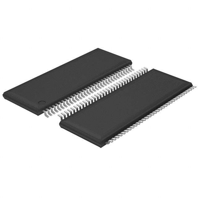
| 产品图片 |
|
| rohs | 符合RoHS无铅 / 符合限制有害物质指令(RoHS)规范要求 |
| 产品系列 | 接口 IC,接口-信号缓冲器、中继器,Texas Instruments SN65LVDS22PW- |
| 数据手册 | |
| 产品型号 | SN65LVDS22PW |
| Tx/Rx类型 | LVDS |
| 产品目录页面 | |
| 产品种类 | 接口-信号缓冲器、中继器 |
| 产品类型 | Repeaters |
| 传播延迟时间 | 4 ns |
| 供应商器件封装 | 16-TSSOP |
| 其它名称 | 296-12024-5 |
| 包装 | 管件 |
| 单位重量 | 60 mg |
| 商标 | Texas Instruments |
| 安装类型 | 表面贴装 |
| 安装风格 | SMD/SMT |
| 封装 | Tube |
| 封装/外壳 | 16-TSSOP(0.173",4.40mm 宽) |
| 封装/箱体 | TSSOP-16 |
| 工作温度 | -40°C ~ 85°C |
| 工作温度范围 | - 40 C to + 85 C |
| 工作电流 | 8 mA |
| 工作电源电压 | 3.3 V |
| 工厂包装数量 | 90 |
| 应用 | - |
| 延迟时间 | 4.0ns |
| 数据速率(最大值) | 250Mbps |
| 最大时钟频率 | 200 MHz |
| 标准包装 | 90 |
| 电压-电源 | 3 V ~ 3.6 V |
| 电容-输入 | 3pF |
| 电流-电源 | 13mA |
| 类型 | 缓冲器, 多路复用器 |
| 系列 | SN65LVDS22 |
| 输入 | LVDS |
| 输出 | LVDS |
| 通道数 | 1 x 2:2 |


- 商务部:美国ITC正式对集成电路等产品启动337调查
- 曝三星4nm工艺存在良率问题 高通将骁龙8 Gen1或转产台积电
- 太阳诱电将投资9.5亿元在常州建新厂生产MLCC 预计2023年完工
- 英特尔发布欧洲新工厂建设计划 深化IDM 2.0 战略
- 台积电先进制程称霸业界 有大客户加持明年业绩稳了
- 达到5530亿美元!SIA预计今年全球半导体销售额将创下新高
- 英特尔拟将自动驾驶子公司Mobileye上市 估值或超500亿美元
- 三星加码芯片和SET,合并消费电子和移动部门,撤换高东真等 CEO
- 三星电子宣布重大人事变动 还合并消费电子和移动部门
- 海关总署:前11个月进口集成电路产品价值2.52万亿元 增长14.8%


PDF Datasheet 数据手册内容提取
SN65LVDS22 SN65LVDM22 www.ti.com SLLS315C–DECEMBER1998–REVISEDJUNE2002 DUAL MULTIPLEXED LVDS REPEATERS FEATURES SN65LVDS22D and SN65LVDS22PW (Marked as LVDS22) • MeetsorExceedstheRequirementsofANSI SN65LVDM22D and SN65LVDM22PW (Marked as LVDM22) (TOP VIEW) TIA/EIA-644-1995Standard • DesignedforClockRatesupto200MHz 1B 1 16 VCC (400Mbps) 1A 2 15 VCC • DesignedforDataRatesupto250Mbps S0 3 14 1Y 1DE 4 13 1Z • PinCompatibleWithSN65LVDS122and S1 5 12 2DE SN65LVDT122,1.5Gbps2x2Crosspoint 2A 6 11 2Z SwitchFromTI 2B 7 10 2Y • ESDProtectionExceeds12kVonBusPins GND 8 9 GND • OperatesFromaSingle3.3-VSupply • Low-VoltageDifferentialSignalingWith logic diagram (positive logic) OutputVoltagesof350mVInto: – 100-W Load(SN65LVDS22) 2 – 50-W Load(SN65LVDM22) 1A + • PropagationDelayTime;4nsTyp 1B 1 _ 0 1143 1Y 1Z • PowerDissipationat400Mbpsof150mW 1 • BusPinsAreHighImpedanceWhenDisabled 4 1DE orWithVCCLessThan1.5V 12 2DE • LVTTLLevelsAre5VTolerant 3 S0 • Open-CircuitFailSafeReceiver 5 DESCRIPTION S1 The SN65LVDS22 and SN65LVDM22 are differential 0 10 2Y line drivers and receivers that use low-voltage 2A 6 + 11 2Z differential signaling (LVDS) to achieve signaling 7 _ 1 2B rates as high as 400 Mbps. The receiver outputs can be switched to either or both drivers through the multiplexer control signals S0 and S1. This allows the MUX TRUTH TABLE flexibility to perform splitter or signal routing functions INPUT OUTPUT withasingledevice. FUNCTION S1 S0 1Y/1Z 2Y/2Z The TIA/EIA-644 standard compliant electrical 0 0 1A/1B 1A/1B Splitter interface provides a minimum differential output 0 1 2A/2B 2A/2B Splitter voltage magnitude of 247 mV into a 100-W load and 1 0 1A/1B 2A/2B Router receipt of 100 mV signals with up to 1 V of ground 1 1 2A/2B 1A/1B Router potential difference between a transmitter and receiver. The SN65LVDM22 doubles the output drive currenttoachieveLVDSlevelswitha50-W load. Pleasebeawarethatanimportantnoticeconcerningavailability,standardwarranty,anduseincriticalapplicationsofTexas Instrumentssemiconductorproductsanddisclaimerstheretoappearsattheendofthisdatasheet. PRODUCTIONDATAinformationiscurrentasofpublicationdate. Copyright©1998–2002,TexasInstrumentsIncorporated Products conform to specifications per the terms of the Texas Instruments standard warranty. Production processing does not necessarilyincludetestingofallparameters.
SN65LVDS22 SN65LVDM22 www.ti.com SLLS315C–DECEMBER1998–REVISEDJUNE2002 The intended application of these devices and signaling technique is for both point-to-point baseband (single termination) and multipoint (double termination) data transmissions over controlled impedance media. The transmission media may be printed-circuit board traces, backplanes, or cables. (Note: The ultimate rate and distanceofdatatransferisdependentupontheattenuationcharacteristicsofthemedia, the noise coupling to the environment,andotherapplicationspecificcharacteristics). TheSN65LVDS22andSN65LVDM22arecharacterizedforoperationfrom–40°Cto85°C. 2 SubmitDocumentationFeedback
SN65LVDS22 SN65LVDM22 www.ti.com SLLS315C–DECEMBER1998–REVISEDJUNE2002 Thesedeviceshavelimitedbuilt-inESDprotection.Theleadsshouldbeshortedtogetherorthedeviceplacedinconductivefoam duringstorageorhandlingtopreventelectrostaticdamagetotheMOSgates. EQUIVALENT INPUT AND OUTPUT SCHEMATIC DIAGRAMS VCC VCC 300 kW 50 W S0, S1 Input 50 W 1DE, 2DE 7 V Input 300 kW 7 V VCC VCC 300 kW 300 kW 5 W Y or Z 10 kW Output A Input B Input 7 V 7 V 7 V ABSOLUTE MAXIMUM RATINGS overoperatingfree-airtemperaturerange(unlessotherwisenoted)(1) UNIT Supplyvoltagerange,V (seeNote (2)) –0.5Vto4V CC (DE,S0,S1) –0.5Vto6V Voltagerange (Y,Z,A,andB) –0.5Vto4V A,B,Y,ZandGND(seeNote (3)) Class3,A:12kV,B:600V Electrostaticdischarge Allpins Class3,A:5kV,B:500V Continuouspowerdissipation SeeDissipationRatingTable Storagetemperaturerange –65°Cto150°C Leadtemperature1,6mm(1/16inch)fromcasefor10seconds 260°C (1) Stressesbeyondthoselistedunderabsolutemaximumratingsmaycausepermanentdamagetothedevice.Thesearestressratings only,andfunctionaloperationofthedeviceattheseoranyotherconditionsbeyondthoseindicatedunderrecommendedoperating conditionsisnotimplied.Exposuretoabsolute-maximum-ratedconditionsforextendedperiodsmayaffectdevicereliability. (2) Allvoltagevalues,exceptdifferentialI/Obusvoltages,arewithrespecttonetworkgroundterminal. (3) TestedinaccordancewithMIL-STD-883CMethod3015.7. SubmitDocumentationFeedback 3
SN65LVDS22 SN65LVDM22 www.ti.com SLLS315C–DECEMBER1998–REVISEDJUNE2002 DISSIPATION RATING TABLE T £ 25°C DERATINGFACTOR(1) T =85°C PACKAGE A A POWERRATING ABOVET =25°C POWERRATING A D 1110mW 8.9mW/°C 577mW PW 839mW 6.7mW/°C 437mW (1) Thisistheinverseofthejunction-to-ambientthermalresistancewhenboard-mountedandwithnoair flow. RECOMMENDED OPERATING CONDITIONS MIN NOM MAX UNIT V Supplyvoltage 3 3.3 3.6 V CC V High-levelinputvoltage S0,S1,1DE,2DE 2 V IH V Low-levelinputvoltage S0,S1,1DE,2DE 0.8 V IL |V | Magnitudeofdifferentialinputvoltage 0.1 0.6 V ID (cid:1) (cid:1) (cid:1) (cid:1) V V V V Common-modeinputvoltage(seeFigure1) ID 2.4– ID IC 2 2 V –0.8 V CC T Operatingfree-airtemperature 40 85 °C A TIMING REQUIREMENTS PARAMETER MIN NOM MAX UNIT t Inputtoselectsetuptime 1.6 ns su t Inputtoselectholdtime SeeFigure6 1 ns h t Selecttoswitchoutput 3.2 5 ns switch COMMON-MODE INPUT VOLTAGE vs DIFFERENTIAL INPUT VOLTAGE 2.5 MAX at VCC > 3.15 V V ge – 2 MAX at VCC = 3 V a olt V ut p 1.5 n e I d o M n- 1 o m m o C – C 0.5 VI Min 0 0 0.1 0.2 0.3 0.4 0.5 0.6 VID – Differential Input Voltage – V Figure1.Common-ModeInputVoltagevsDifferentialInputVoltage 4 SubmitDocumentationFeedback
SN65LVDS22 SN65LVDM22 www.ti.com SLLS315C–DECEMBER1998–REVISEDJUNE2002 RECEIVER ELECTRICAL CHARACTERISTICS overrecommendedoperatingconditions(unlessotherwisenoted) PARAMETER TESTCONDITIONS MIN TYP MAX UNIT V Positive-goingdifferentialinputvoltagethreshold 100 mV IT+ V Negative-goingdifferentialinputvoltagethreshold 100 mV IT– V =0V 2 20 I I Inputcurrent(AorBinputs) µA I V =2.4V 1.2 I I I(OFF Power-offinputcurrent(AorBinputs) V =0V 20 µA CC ) RECEIVER/DRIVER ELECTRICAL CHARACTERISTICS overrecommendedoperatingconditions(unlessotherwisenoted) PARAMETER TESTCONDITIONS MIN TYP(1) MAX UNIT V Differentialoutputvoltagemagnitude 247 340 454 mV OD D V Changeindifferentialoutputvoltagemagnitude SeeFigure2 –50 50 mV OD betweenlogicstates R =100W ('LVDS22), 1.37 VOC(SS) Steady-statecommon-modeoutputvoltage RL=50W ('LVDM22) 1.125 5 V L D V Changeinsteady-statecommon-modeoutput SeeFigure3 –50 3 50 mV OC(SS) voltagebetweenlogicstates V Peak-to-peakcommon-modeoutputvoltage 150 mV OC(PP) NoLoad 8 12 R =100W ('LVDS22) 13 20 L I Supplycurrent mA CC R =50W ('LVDM22) 21 27 L Disabled 3 6 DE –10 I High-levelinputcurrent V =5V µA IH IH S0,S1 20 DE –10 I Low-levelinputcurrent V =0.8V µA IL IL S0,S1 10 –10 V orV =0V,V =0V('LVDS22) OY OZ OD –10 I Short-circuitoutputcurrent mA OS –10 V orV =0V,V =0V('LVDM22) OY OZ OD –10 V =600mV 0.015 ±1 OD I High-impedanceoutputcurrent µA OZ V =0VorV 0.015 ±1 O CC I Power-offoutputcurrent V =0V, V =3.6V 0.015 ±1 µA O(OFF) CC O C Inputcapacitance 3 pF IN (1) Alltypicalvaluesareat25°Candwitha3.3-Vsupply. SubmitDocumentationFeedback 5
SN65LVDS22 SN65LVDM22 www.ti.com SLLS315C–DECEMBER1998–REVISEDJUNE2002 DIFFERENTIAL RECEIVER TO DRIVER SWITCHING CHARACTERISTICS overrecommendedoperatingconditions(unlessotherwisenoted) PARAMETER TESTCONDITIONS MIN TYP(1) MAX UNIT t Differentialpropagationdelaytime,low-to-high 4 6 ns PLH t Differentialpropagationdelaytime,high-to-low 4 6 ns PHL t Pulseskew(|t -t |) 0.2 ns sk(p) PHL PLH t Transitiontime,low-to-high SN65LVDS22 C =10pF,SeeFigure4 1 1.5 ns r L t Transitiontime,low-to-high SN65LVDM22 0.8 1.3 ns r t Transitiontime,high-to-low SN65LVDS22 1 1.5 ns f t Transitiontime,high-to-low SN65LVDM22 0.8 1.3 ns f t Propagationdelaytime,high-level-to-high-impedanceoutput 4 10 ns PHZ t Propagationdelaytime,low-level-to-high-impedanceoutput 5 10 ns PLZ SeeFigure5 t Propagationdelaytime,high-impedance-to-high-leveloutput 5 10 ns PZH t Propagationdelaytime,high-impedance-to-low-leveloutput 6 10 ns PZL t 0.2 PHL_R1_Dx t 0.2 PLH_R1_Dx Channel-to-channelskew,receivertodriver(2) ns t 0.2 PHL_R2_Dx t 0.2 PLH_R2_Dx f Maximumoperatingfrequency Allchannelsswitching 200 MHz max (1) Alltypicalvaluesareat25°Candwitha3.3-Vsupply. (2) Theseparametricvaluesaremeasuredoversupplyvoltageandtemperaturerangesrecommendedforthedevice. PARAMETER MEASUREMENT INFORMATION DE A Y Pulse Generator VOD RL (see Note B) Z B Input (see Note A) CL = 10 pF (2 Places) (see Note C) VI(B) 1.4 V 100% 80% VI(A) 1 V VOD 0 20% 0% tf tr A. All input pulses are supplied by a generator having the following characteristics: t or t £ 1 ns, pulse repetition rate r f (PRR)=50Mpps,pulsewidth=10±0.2ns. B. R =100W or50W ±1% L C. C includesinstrumentationandfixturecapacitancewithin6mmoftheD.U.T. L Figure2.TestCircuitandVoltageDefinitionsfortheDifferentialOutputSignal 6 SubmitDocumentationFeedback
SN65LVDS22 SN65LVDM22 www.ti.com SLLS315C–DECEMBER1998–REVISEDJUNE2002 PARAMETER MEASUREMENT INFORMATION (continued) DE RL (see Note B) (2 Places) VI(B) 1.4 V A Y Pulse VI(A) 1 V Generator B Input Z VOC(PP) (see Note A) VOC (see Note D) VOC(SS) CL = 10 pF (2 Places) (see Note C) VCC A. All input pulses are supplied by a generator having the following characteristics: t or t £ 1 ns, pulse repetition rate r f (PRR)=50Mpps,pulsewidth=10±0.2ns. B. R =100W or50W ±1% L C. C includesinstrumentationandfixturecapacitancewithin6mmoftheD.U.T. L D. ThemeasurementofV ismadeontestequipmentwitha-3dBbandwidthofatleast300MHz. OC(PP) Figure3.TestCircuitandDefinitionsfortheDriverCommon-ModeOutputVoltage DE A Y Pulse Generator R D RL (see Note A) B Z 10 pF 10 pF VIB 1.4 V 0-V Differential 1.2-V CM VIA 1 V tPLH tPHL VOZ 1.4 V 0-V Differential 1.2-V CM VOY 1 V 80% 0-V Differential 20% VOY – VOZ tr tf A. R =100W or50W ±1% L B. All input pulses are supplied by a generator having the following characteristics: pulse repetition rate (PRR) = 50 Mpps,pulsewidth=10±0.2ns. Figure4.DifferentialReceivertoDriverPropagationDelayandDriverTransitionTimeWaveforms SubmitDocumentationFeedback 7
SN65LVDS22 SN65LVDM22 www.ti.com SLLS315C–DECEMBER1998–REVISEDJUNE2002 PARAMETER MEASUREMENT INFORMATION (continued) DE RL/2 A (see Note A) 1 V or 1.4 V R D 1.2 V 1.2 V B RL/2 (see Note A) 2 V DE 1.4 V 0.8 V tPZH tPHZ ≈1.4 V VOY or VOZ 1.25 V 1.2 V tPZL tPLZ 1.2 V VOY or VOZ 1.15 V ≈1 V A. R =100W or50W ±1% L B. All input pulses are supplied by a generator having the following characteristics: pulse repetition rate (PRR) = 0.5 Mpps,pulsewidth=500±10ns. Figure5.EnableandDisableTimingCircuit 8 SubmitDocumentationFeedback
SN65LVDS22 SN65LVDM22 www.ti.com SLLS315C–DECEMBER1998–REVISEDJUNE2002 PARAMETER MEASUREMENT INFORMATION (continued) 1A/B 2A/B tsu th S0/1 Outputs Out 1 or 2 Out 1 or 2 tsu DE NOTE: tsu and th times specify that data must be in a stable state before and after MUX control switches. Figure6.Input-to-SelectforBothRisingandFallingEdgeSetupandHoldTimes SubmitDocumentationFeedback 9
SN65LVDS22 SN65LVDM22 www.ti.com SLLS315C–DECEMBER1998–REVISEDJUNE2002 TYPICAL CHARACTERISTICS SN65LVDS22 SN65LVDS22 HIGH-LEVELOUTPUTVOLTAGE LOW-LEVELOUTPUTVOLTAGE vs vs HIGH-LEVELOUTPUTCURRENT LOW-LEVELOUTPUTCURRENT 3.5 4 VCC = 3.3 V TA = 25°C VCC = 3.3 V V 3 − V TA = 25°C − e ge ag 3 olta 2.5 Volt ut V put pt 2 ut u O vel O 1.5 evel 2 e L h-L ow- g L Hi 1 − − L 1 H O O V V .5 0 0 −4 −3 −2 −1 0 0 2 4 6 IOH − High-Level Output Current − mA IOL − Low-Level Output Current − mA Figure7. Figure8. SN65LVDM22 SN65LVDM22 HIGH-LEVELOUTPUTVOLTAGE LOW-LEVELOUTPUTVOLTAGE vs vs HIGH-LEVELOUTPUTCURRENT LOW-LEVELOUTPUTCURRENT 3.5 4 VTAC C= =2 53°.C3 V VTAC C= =2 53°.C3 V 3 V V − − e e 3 g g a 2.5 a olt olt V V put 2 put ut ut O O 2 vel 1.5 vel e e L L h- w- Hig 1 Lo − − 1 H L O O V .5 V 0 0 −8 −6 −4 −2 0 0 2 4 6 8 10 12 IOH − High-Level Output Current − mA IOL − Low-Level Output Current − mA Figure9. Figure10. 10 SubmitDocumentationFeedback
SN65LVDS22 SN65LVDM22 www.ti.com SLLS315C–DECEMBER1998–REVISEDJUNE2002 APPLICATION INFORMATION FAIL SAFE One of the most common problems with differential signaling applications is how the system responds when no differential voltage is present on the signal pair. The LVDS receiver is like most differential line receivers, in that its output logic state can be indeterminate when the differential input voltage is between –100 mV and 100mV and within its recommended input common-mode voltage range. However, TI's LVDS receiver is different in how ithandlestheopen-inputcircuitsituation. Open-circuit means that there is little or no input current to the receiver from the data line itself. This could be when the driver is in a high-impedance state or the cable is disconnected. When this occurs, the LVDS receiver pulls each line of the signal pair to near V through 300-kW resistors as shown in Figure 11. The fail-safe CC feature uses an AND gate with input voltage thresholds at about 2.3 V to detect this condition and force the outputtoahigh-levelregardlessofthedifferentialinputvoltage. VCC 300 kW 300 kW A Rt = 100 W (Typ) Y B VIT ≈ 2.3 V Figure11.Open-CircuitFailSafeoftheLVDSReceiver It is only under these conditions that the output of the receiver is valid with less than a 100 mV differential input voltagemagnitude.Thepresenceoftheterminationresistor,Rt,does not affect the fail-safe function as long as it isconnected as shown in Figure 11. Other termination circuits may allow a dc current to ground that could defeat thepullupcurrentsfromthereceiverandthefail-safefeature. SubmitDocumentationFeedback 11
PACKAGE OPTION ADDENDUM www.ti.com 26-Aug-2009 PACKAGING INFORMATION OrderableDevice Status(1) Package Package Pins Package EcoPlan(2) Lead/BallFinish MSLPeakTemp(3) Type Drawing Qty SN65LVDM22D ACTIVE SOIC D 16 40 Green(RoHS& CUNIPDAU Level-1-260C-UNLIM noSb/Br) SN65LVDM22DG4 ACTIVE SOIC D 16 40 Green(RoHS& CUNIPDAU Level-1-260C-UNLIM noSb/Br) SN65LVDM22PW ACTIVE TSSOP PW 16 90 Green(RoHS& CUNIPDAU Level-1-260C-UNLIM noSb/Br) SN65LVDM22PWG4 ACTIVE TSSOP PW 16 90 Green(RoHS& CUNIPDAU Level-1-260C-UNLIM noSb/Br) SN65LVDS22D ACTIVE SOIC D 16 40 Green(RoHS& CUNIPDAU Level-1-260C-UNLIM noSb/Br) SN65LVDS22DG4 ACTIVE SOIC D 16 40 Green(RoHS& CUNIPDAU Level-1-260C-UNLIM noSb/Br) SN65LVDS22DR ACTIVE SOIC D 16 2500 Green(RoHS& CUNIPDAU Level-1-260C-UNLIM noSb/Br) SN65LVDS22DRG4 ACTIVE SOIC D 16 2500 Green(RoHS& CUNIPDAU Level-1-260C-UNLIM noSb/Br) SN65LVDS22PW ACTIVE TSSOP PW 16 90 Green(RoHS& CUNIPDAU Level-1-260C-UNLIM noSb/Br) SN65LVDS22PWG4 ACTIVE TSSOP PW 16 90 Green(RoHS& CUNIPDAU Level-1-260C-UNLIM noSb/Br) SN65LVDS22PWR ACTIVE TSSOP PW 16 2000 Green(RoHS& CUNIPDAU Level-1-260C-UNLIM noSb/Br) SN65LVDS22PWRG4 ACTIVE TSSOP PW 16 2000 Green(RoHS& CUNIPDAU Level-1-260C-UNLIM noSb/Br) (1)Themarketingstatusvaluesaredefinedasfollows: ACTIVE:Productdevicerecommendedfornewdesigns. LIFEBUY:TIhasannouncedthatthedevicewillbediscontinued,andalifetime-buyperiodisineffect. NRND:Notrecommendedfornewdesigns.Deviceisinproductiontosupportexistingcustomers,butTIdoesnotrecommendusingthispartin anewdesign. PREVIEW:Devicehasbeenannouncedbutisnotinproduction.Samplesmayormaynotbeavailable. OBSOLETE:TIhasdiscontinuedtheproductionofthedevice. (2)EcoPlan-Theplannedeco-friendlyclassification:Pb-Free(RoHS),Pb-Free(RoHSExempt),orGreen(RoHS&noSb/Br)-pleasecheck http://www.ti.com/productcontentforthelatestavailabilityinformationandadditionalproductcontentdetails. TBD:ThePb-Free/Greenconversionplanhasnotbeendefined. Pb-Free(RoHS):TI'sterms"Lead-Free"or"Pb-Free"meansemiconductorproductsthatarecompatiblewiththecurrentRoHSrequirements forall6substances,includingtherequirementthatleadnotexceed0.1%byweightinhomogeneousmaterials.Wheredesignedtobesoldered athightemperatures,TIPb-Freeproductsaresuitableforuseinspecifiedlead-freeprocesses. Pb-Free(RoHSExempt):ThiscomponenthasaRoHSexemptionforeither1)lead-basedflip-chipsolderbumpsusedbetweenthedieand package, or 2) lead-based die adhesive used between the die and leadframe. The component is otherwise considered Pb-Free (RoHS compatible)asdefinedabove. Green(RoHS&noSb/Br):TIdefines"Green"tomeanPb-Free(RoHScompatible),andfreeofBromine(Br)andAntimony(Sb)basedflame retardants(BrorSbdonotexceed0.1%byweightinhomogeneousmaterial) (3) MSL, Peak Temp. -- The Moisture Sensitivity Level rating according to the JEDEC industry standard classifications, and peak solder temperature. Important Information and Disclaimer:The information provided on this page represents TI's knowledge and belief as of the date that it is provided. TI bases its knowledge and belief on information provided by third parties, and makes no representation or warranty as to the accuracy of such information. Efforts are underway to better integrate information from third parties. TI has taken and continues to take reasonable steps to provide representative and accurate information but may not have conducted destructive testing or chemical analysis on incomingmaterialsandchemicals.TIandTIsuppliersconsidercertaininformationtobeproprietary,andthusCASnumbersandotherlimited informationmaynotbeavailableforrelease. Addendum-Page1
PACKAGE OPTION ADDENDUM www.ti.com 26-Aug-2009 InnoeventshallTI'sliabilityarisingoutofsuchinformationexceedthetotalpurchasepriceoftheTIpart(s)atissueinthisdocumentsoldbyTI toCustomeronanannualbasis. Addendum-Page2
PACKAGE MATERIALS INFORMATION www.ti.com 25-Sep-2009 TAPE AND REEL INFORMATION *Alldimensionsarenominal Device Package Package Pins SPQ Reel Reel A0 B0 K0 P1 W Pin1 Type Drawing Diameter Width (mm) (mm) (mm) (mm) (mm) Quadrant (mm) W1(mm) SN65LVDS22DR SOIC D 16 2500 330.0 16.4 6.5 10.3 2.1 8.0 16.0 Q1 SN65LVDS22PWR TSSOP PW 16 2000 330.0 12.4 6.9 5.6 1.6 8.0 12.0 Q1 PackMaterials-Page1
PACKAGE MATERIALS INFORMATION www.ti.com 25-Sep-2009 *Alldimensionsarenominal Device PackageType PackageDrawing Pins SPQ Length(mm) Width(mm) Height(mm) SN65LVDS22DR SOIC D 16 2500 346.0 346.0 33.0 SN65LVDS22PWR TSSOP PW 16 2000 346.0 346.0 29.0 PackMaterials-Page2
IMPORTANTNOTICE TexasInstrumentsIncorporatedanditssubsidiaries(TI)reservetherighttomakecorrections,modifications,enhancements,improvements, andotherchangestoitsproductsandservicesatanytimeandtodiscontinueanyproductorservicewithoutnotice.Customersshould obtainthelatestrelevantinformationbeforeplacingordersandshouldverifythatsuchinformationiscurrentandcomplete.Allproductsare soldsubjecttoTI’stermsandconditionsofsalesuppliedatthetimeoforderacknowledgment. TIwarrantsperformanceofitshardwareproductstothespecificationsapplicableatthetimeofsaleinaccordancewithTI’sstandard warranty.TestingandotherqualitycontroltechniquesareusedtotheextentTIdeemsnecessarytosupportthiswarranty.Exceptwhere mandatedbygovernmentrequirements,testingofallparametersofeachproductisnotnecessarilyperformed. TIassumesnoliabilityforapplicationsassistanceorcustomerproductdesign.Customersareresponsiblefortheirproductsand applicationsusingTIcomponents.Tominimizetherisksassociatedwithcustomerproductsandapplications,customersshouldprovide adequatedesignandoperatingsafeguards. TIdoesnotwarrantorrepresentthatanylicense,eitherexpressorimplied,isgrantedunderanyTIpatentright,copyright,maskworkright, orotherTIintellectualpropertyrightrelatingtoanycombination,machine,orprocessinwhichTIproductsorservicesareused.Information publishedbyTIregardingthird-partyproductsorservicesdoesnotconstitutealicensefromTItousesuchproductsorservicesora warrantyorendorsementthereof.Useofsuchinformationmayrequirealicensefromathirdpartyunderthepatentsorotherintellectual propertyofthethirdparty,oralicensefromTIunderthepatentsorotherintellectualpropertyofTI. ReproductionofTIinformationinTIdatabooksordatasheetsispermissibleonlyifreproductioniswithoutalterationandisaccompanied byallassociatedwarranties,conditions,limitations,andnotices.Reproductionofthisinformationwithalterationisanunfairanddeceptive businesspractice.TIisnotresponsibleorliableforsuchaltereddocumentation.Informationofthirdpartiesmaybesubjecttoadditional restrictions. ResaleofTIproductsorserviceswithstatementsdifferentfromorbeyondtheparametersstatedbyTIforthatproductorservicevoidsall expressandanyimpliedwarrantiesfortheassociatedTIproductorserviceandisanunfairanddeceptivebusinesspractice.TIisnot responsibleorliableforanysuchstatements. TIproductsarenotauthorizedforuseinsafety-criticalapplications(suchaslifesupport)whereafailureoftheTIproductwouldreasonably beexpectedtocauseseverepersonalinjuryordeath,unlessofficersofthepartieshaveexecutedanagreementspecificallygoverning suchuse.Buyersrepresentthattheyhaveallnecessaryexpertiseinthesafetyandregulatoryramificationsoftheirapplications,and acknowledgeandagreethattheyaresolelyresponsibleforalllegal,regulatoryandsafety-relatedrequirementsconcerningtheirproducts andanyuseofTIproductsinsuchsafety-criticalapplications,notwithstandinganyapplications-relatedinformationorsupportthatmaybe providedbyTI.Further,BuyersmustfullyindemnifyTIanditsrepresentativesagainstanydamagesarisingoutoftheuseofTIproductsin suchsafety-criticalapplications. TIproductsareneitherdesignednorintendedforuseinmilitary/aerospaceapplicationsorenvironmentsunlesstheTIproductsare specificallydesignatedbyTIasmilitary-gradeor"enhancedplastic."OnlyproductsdesignatedbyTIasmilitary-grademeetmilitary specifications.BuyersacknowledgeandagreethatanysuchuseofTIproductswhichTIhasnotdesignatedasmilitary-gradeissolelyat theBuyer'srisk,andthattheyaresolelyresponsibleforcompliancewithalllegalandregulatoryrequirementsinconnectionwithsuchuse. TIproductsareneitherdesignednorintendedforuseinautomotiveapplicationsorenvironmentsunlessthespecificTIproductsare designatedbyTIascompliantwithISO/TS16949requirements.Buyersacknowledgeandagreethat,iftheyuseanynon-designated productsinautomotiveapplications,TIwillnotberesponsibleforanyfailuretomeetsuchrequirements. FollowingareURLswhereyoucanobtaininformationonotherTexasInstrumentsproductsandapplicationsolutions: Products Applications Amplifiers amplifier.ti.com Audio www.ti.com/audio DataConverters dataconverter.ti.com Automotive www.ti.com/automotive DLP®Products www.dlp.com Broadband www.ti.com/broadband DSP dsp.ti.com DigitalControl www.ti.com/digitalcontrol ClocksandTimers www.ti.com/clocks Medical www.ti.com/medical Interface interface.ti.com Military www.ti.com/military Logic logic.ti.com OpticalNetworking www.ti.com/opticalnetwork PowerMgmt power.ti.com Security www.ti.com/security Microcontrollers microcontroller.ti.com Telephony www.ti.com/telephony RFID www.ti-rfid.com Video&Imaging www.ti.com/video RF/IFandZigBee®Solutions www.ti.com/lprf Wireless www.ti.com/wireless MailingAddress:TexasInstruments,PostOfficeBox655303,Dallas,Texas75265 Copyright©2009,TexasInstrumentsIncorporated