
 Datasheet下载
- 型号: SMCJ26CA
- 制造商: Bourns
- 库位|库存: xxxx|xxxx
- 要求:
| 数量阶梯 | 香港交货 | 国内含税 |
| +xxxx | $xxxx | ¥xxxx |
查看当月历史价格
查看今年历史价格
SMCJ26CA产品简介:
ICGOO电子元器件商城为您提供SMCJ26CA由Bourns设计生产,在icgoo商城现货销售,并且可以通过原厂、代理商等渠道进行代购。 SMCJ26CA价格参考。BournsSMCJ26CA封装/规格:TVS - 二极管, 。您可以下载SMCJ26CA参考资料、Datasheet数据手册功能说明书,资料中有SMCJ26CA 详细功能的应用电路图电压和使用方法及教程。
SMCJ26CA 是由 ON Semiconductor(安森美半导体)生产的一款 TVS(瞬态电压抑制器)二极管,属于 SMC 系列。其主要功能是保护电路免受瞬态电压尖峰的影响,例如静电放电(ESD)、电感负载开关和雷击浪涌等。以下是 SMCJ26CA 的典型应用场景:

 1. 电源线保护
   - SMCJ26CA 可用于保护交流或直流电源输入端口,防止因电压波动、雷击或其他外部干扰导致的损坏。
   - 适用于工业设备、家用电器和消费电子产品的电源接口。

 2. 数据线和信号线保护
   - 在通信接口中(如 USB、RS-232、RS-485、CAN 总线等),SMCJ26CA 能有效抑制信号线上可能出现的瞬态电压。
   - 特别适合高速数据传输场景,确保信号完整性并延长设备寿命。

 3. 汽车电子系统
   - 在汽车电子中,SMCJ26CA 可用于保护车载音响、导航系统、传感器和其他控制模块的电路。
   - 抵抗汽车环境中常见的电压浪涌(如启动电机时产生的瞬态电压)。

 4. 电机驱动保护
   - 在电机驱动电路中,当电感性负载切换时会产生反向电动势(电压尖峰)。SMCJ26CA 可以吸收这些尖峰电压,保护驱动电路中的其他元件。

 5. 消费电子产品
   - 用于手机充电器、笔记本电脑适配器、电视等消费电子产品的输入/输出端口保护。
   - 防止因插拔操作或外部环境因素引起的 ESD 或浪涌损坏。

 6. 工业自动化设备
   - 在工业控制系统中,SMCJ26CA 可保护 PLC(可编程逻辑控制器)、继电器和其他关键组件免受电压浪涌影响。
   - 提高设备的可靠性和稳定性,减少维护成本。

 7. 电信设备
   - 在基站、路由器、交换机等电信设备中,SMCJ26CA 能有效保护天线接口、电源输入和其他敏感电路部分。
   - 确保设备在恶劣电磁环境下正常运行。

 产品特性:
- 最大反向工作电压:26V
- 峰值脉冲功率:1500W(10/1000μs 波形)
- 响应时间:极快(通常小于 1ps),能够迅速抑制瞬态电压。
- 封装形式:DO-214AC(SMC 封装),便于表面贴装和散热。

综上所述,SMCJ26CA 广泛应用于需要高可靠性电压保护的场合,尤其是在电力、通信、汽车和工业领域中,为电路提供有效的瞬态电压防护。
| 参数 | 数值 |
| 产品目录 | |
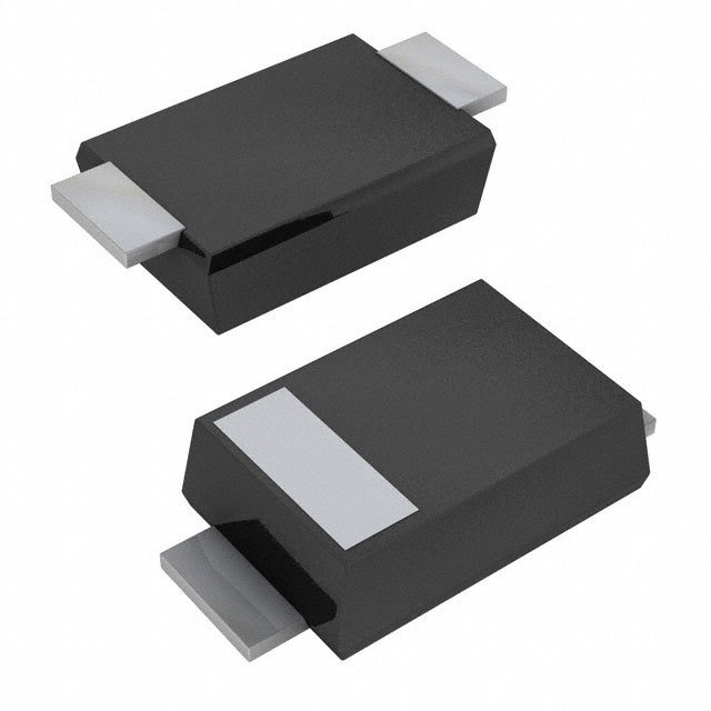
| 描述 | TVS DIODE 26VWM SMDTVS 二极管 - 瞬态电压抑制器 26volts 5uA 35.6 Amps Bi-Dir |
| 产品分类 | |
| 品牌 | Bourns |
| 产品手册 | |
| 产品图片 |
|
| rohs | RoHS 合规性豁免不受无铅要求限制 / 符合限制有害物质指令(RoHS)规范要求 |
| 产品系列 | 二极管与整流器,TVS二极管,TVS 二极管 - 瞬态电压抑制器,Bourns SMCJ26CASMCJ |
| 数据手册 | |
| 产品型号 | SMCJ26CA |
| RoHS指令信息 | |
| 不同频率时的电容 | - |
| 产品目录绘图 |
|
| 产品目录页面 | |
| 产品种类 | TVS 二极管 - 瞬态电压抑制器 |
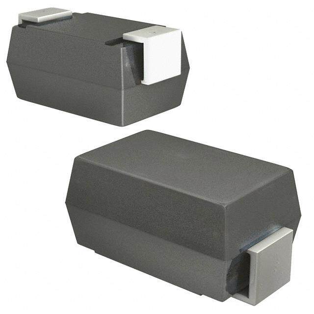
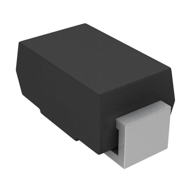
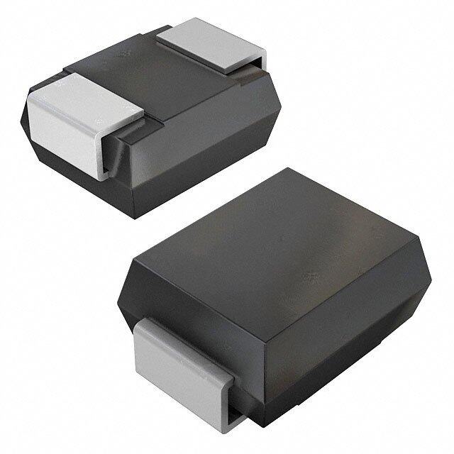
| 供应商器件封装 | SMC (DO-214AB) |
| 其它名称 | SMCJ26CABTR |
| 击穿电压 | 28.9 V to 32.2 V |
| 功率-峰值脉冲 | 1500W (1.5kW) |
| 包装 | 带卷 (TR) |
| 单向通道 | - |
| 双向通道 | 1 |
| 商标 | Bourns |
| 安装类型 | 表面贴装 |
| 安装风格 | SMD/SMT |
| 封装 | Reel |
| 封装/外壳 | DO-214AB,SMC |
| 封装/箱体 | DO-214AB |
| 尺寸 | 5.59 mm W x 7.11 mm L x 2.62 mm H |
| 峰值浪涌电流 | 200 A |
| 峰值脉冲功率耗散 | 1.5 kW |
| 工作温度 | -55°C ~ 150°C |
| 工作电压 | 3.5 V |
| 工厂包装数量 | 3000 |
| 应用 | 通用 |
| 最大工作温度 | + 150 C |
| 最小工作温度 | - 55 C |
| 极性 | Bidirectional |
| 标准包装 | 3,000 |
| 特色产品 | http://www.digikey.com/product-highlights/cn/zh/bourns-smx-tvs-diodes/1448 |
| 电压-击穿(最小值) | 28.9V |
| 电压-反向关态(典型值) | 26V |
| 电压-箝位(最大值)@Ipp | - |
| 电流-峰值脉冲(10/1000µs) | - |
| 电源线路保护 | 无 |
| 端接类型 | SMD/SMT |
| 类型 | 齐纳 |
| 系列 | SMCJ |


PDF Datasheet 数据手册内容提取
FAIRCHILD TVS Is Now Part of To learn more about Taiwan Semiconductor, please visit our website at www.taiwansemi.com Please note: The acquisition of this portfolio aligns with our strategy to expand in power semiconductor applications while strengthening our core circuit protection business. All of the Fairchild orderable part numbers will remain unchanged in order to maintain consistency with our customers. For more information regarding this acquisition please refer to ON Semi / Fairchild TVS Acquisition Q&A Version: A1806
S M C J 5 V 0 ( C ) A SMCJ5V0(C)A - SMCJ170(C)A - S M 1500 Watt Transient Voltage Suppressors C J 1 7 0 ( C Features ) A — • Glass-Passivated Junction • 1500 W Peak Pulse Power Capability 1 5 on 10/1000 μs Waveform. 0 0 • Excellent Clamping Capability W • Low-Incremental Surge Resistance a t • Fast Response Time: Typically Less than 1.0 ps from 0 V SMC/DO-214AB t T to BV Minimum for Unidirectional and 5.0 ns for Bidirectional Band denotes cathode on unidirectional devices only. r No band on bi-directional devices. Bi-directional types a • Typical I Less than 1.0 μA Above 10 V have CA suffix where electrical characteristics apply in n R both directions suitable for bi-directional applications. s • UL Certificate #E258596 ie n • UL94V-0 Flammability Classification t V o l t a g e S u Absolute Maximum Ratings p p r Stresses exceeding the absolute maximum ratings may damage the device. The device may not function or be opera- e s ble above the recommended operating conditions and stressing the parts to these levels is not recommended. In addi- s tion, extended exposure to stresses above the recommended operating conditions may affect device reliability. The o r absolute maximum ratings are stress ratings only. Values are at T = 25°C unless otherwise noted. s A Symbol Parameter Value Unit P Peak Pulse Power Dissipation on 10/1000 μs Waveform 1500 W PPM I Peak Pulse Current on 10/1000 μs Waveform See table A PPM Non-Repetitive Peak Forward Surge Current I 200 A FSM Superimposed on Rated Load (JEDEC Method)(1) T Storage Temperature Range -55 to 150 °C STG T Operating Junction Temperature 150 °C J Note: 1.Measured on 8.3 ms single half-sine wave or equivalent square wave: duty cycle = 4 pulses per minute maximum. SMCJ5V0(C)A - SMCJ170(C)A Version: A1806
S M Electrical Characteristics C J Values are at T = 25°C unless otherwise noted. 5 A V 0 Reverse Breakdown Clamping Reverse ( Uni-Directional Test Peak Pulse C Part Stand-Off Voltage Voltage Leakage ) Bi-DirDeecvtiiocneal (C) Marking(2) VVRoWltMa g(Ve ) MinV.BR (MV)ax. CITu (rmreAn)t aVtC I P(PVM) ICPuPMrr e(Ant) IaRt (VμRAW)(M3) A - S M SMCJ5V0(C)A GDE 5.0 6.40 7.00 10 9.2 163.0 1000 C SMCJ6V0(C)A GDG 6.0 6.67 7.37 10 10.3 145.6 1000 J 1 SMCJ6V5(C)A GDK 6.5 7.22 7.98 10 11.2 133.9 500 7 0 SMCJ7V0(C)A GDM 7.0 7.78 8.60 10 12.0 125.0 200 ( C SMCJ7V5(C)A GDP 7.5 8.33 9.21 1 12.9 116.3 100 )A SMCJ8V0(C)A GDR 8.0 8.89 9.83 1 13.6 110.3 50 — SMCJ8V5(C)A GDT 8.5 9.44 10.4 1 14.4 104.2 20 1 5 SMCJ9V0(C)A GDV 9.0 10.0 11.1 1 15.4 97.4 10 0 0 SMCJ10(C)A GDX 10 11.1 12.3 1 17.0 88.2 5 W SMCJ11(C)A GDZ 11 12.2 13.5 1 18.2 82.4 5 a t SMCJ12(C)A GEE 12 13.3 14.7 1 19.9 75.3 5 t T SMCJ13(C)A GEG 13 14.4 15.9 1 21.5 69.8 5 ra n SMCJ14(C)A GEK 14 15.6 17.2 1 23.2 64.7 5 s i SMCJ15(C)A GEM 15 16.7 18.5 1 24.4 61.5 5 e n SMCJ16(C)A GEP 16 17.8 19.7 1 26.0 57.7 5 t V SMCJ17(C)A GER 17 18.9 20.9 1 27.6 54.3 5 o l t SMCJ18(C)A GET 18 20.0 22.1 1 29.2 51.4 5 a g SMCJ20(C)A GEV 20 22.2 24.5 1 32.4 46.3 5 e S SMCJ22(C)A GEX 22 24.4 26.9 1 35.5 42.3 5 u p SMCJ24(C)A GEZ 24 26.7 29.5 1 38.9 38.6 5 p r SMCJ26(C)A GFE 26 28.9 31.9 1 42.1 35.6 5 e s SMCJ28(C)A GFG 28 31.1 34.4 1 45.4 33.0 5 s o SMCJ30(C)A GFK 30 33.3 36.8 1 48.4 31.0 5 r s SMCJ33(C)A GFM 33 36.7 40.6 1 53.3 28.1 5 SMCJ36(C)A GFP 36 40.0 44.2 1 58.1 25.8 5 SMCJ40(C)A GFR 40 44.4 49.1 1 64.5 23.3 5 SMCJ43(C)A GFT 43 47.8 52.8 1 69.4 21.6 5 SMCJ45(C)A GFV 45 50.0 55.3 1 72.7 20.6 5 SMCJ48(C)A GFX 48 53.3 58.9 1 77.4 19.4 5 SMCJ51(C)A GFZ 51 56.7 62.7 1 82.4 18.2 5 SMCJ54(C)A GGE 54 60.0 66.3 1 87.1 17.2 5 SMCJ58(C)A GGG 58 64.4 71.2 1 93.6 16.0 5 SMCJ60(C)A GGK 60 66.7 73.7 1 96.8 15.5 5 SMCJ64(C)A GGM 64 71.1 78.6 1 103.0 14.6 5 SMCJ70(C)A GGP 70 77.8 86.0 1 113.0 13.3 5 SMCJ75(C)A GGR 75 83.3 92.1 1 121.0 12.4 5 SMCJ78(C)A GGT 78 86.7 95.8 1 126.0 11.9 5 Notes: 2.Color band denotes cathode on unidirectional devices only. No color band on bidirectional devices. 3.For bidirectional parts with V < 10 V, the I max limit is doubled. RWM R SMCJ5V0(C)A - SMCJ170(C)A 2 Version: A1806
S M Electrical Characteristics (Continued) C J Values are at T = 25°C unless otherwise noted. 5 A V 0 Reverse Breakdown Clamping Reverse (C Uni-Directional Test Peak Pulse Part Stand-Off Voltage Voltage Leakage ) Bi-Directional (C) Current Current A Device Marking(2) Voltage VBR (V) I (mA) at IPPM I (A) at VRWM - VRWM (V) Min. Max. T VC (V) PPM IR (μA)(3) S M SMCJ85(C)A GGV 85 94.4 104.0 1 137.0 10.9 5 C SMCJ90(C)A GGX 90 100.0 111.0 1 146.0 10.3 5 J 1 SMCJ100(C)A GGZ 100 111.0 123.0 1 162.0 9.3 5 7 0 SMCJ110(C)A GHE 110 122.0 135.0 1 177.0 8.5 5 (C ) SMCJ120(C)A GHG 120 133.0 147.0 1 193.0 7.8 5 A SMCJ130(C)A GHK 130 144.0 159.0 1 209.0 7.2 5 — SMCJ150(C)A GHM 150 167.0 185.0 1 243.0 6.2 5 1 5 SMCJ160(C)A GHP 160 178.0 197.0 1 259.0 5.8 5 0 0 SMCJ170(C)A GHR 170 189.0 209.0 1 275.0 5.5 5 W a Notes: t t 2.Color band denotes cathode on unidirectional devices only. No color band on bidirectional devices. T r 3.For bidirectional parts with V < 10 V, the I max limit is doubled. a RWM R n s i e n t V o l t a g e S u p p r e s s o r s SMCJ5V0(C)A - SMCJ170(C)A 3 Version: A1806
S M Typical Performance Characteristics C J 5 V 0 ( C 100 ) 100 A - S R (kW) 10 TA = 25 º C R (%) 75 MC E E J W W 1 O O 50 7 LSE P 1 LSE P 0(C PU PU 25 )A — 0.1 0 1 0.0001 0.001 0.01 0.1 1 10 0 25 50 75 100 125 150 175 200 5 PULSE WIDTH (ms) AMBIENT TEMPERATURE (º C) 0 0 W Figure 1. Peak Pulse Power Rating Curve Figure 2. Pulse Derating Curve a t t T URRENT (%)110500 PItpfe p=am k1 0V μμμμa sluece CPaTs Auu rl t=srh ee2en 5WPt º DoiCdientcht a W(ytdsh) et iorse 5D t0he%efi noPefe daIpkp CE (pF)12100000000000 VTf i =As g=1 MZ . 2=0ee 5 5rMa ºo 0sHC mBu z ri aeV sdp - ap t ransient V C Half Value-Ipp N o AK PULSE 50 a10s /21D 0 e 0 fi0nμμμμesde bc yW Ra.vEe.Afo.r m CAPACITA 100 MSVtoealantsadug-Oree fd(fV aR tW M ) ltage S PE e-kt u td p p 0 0 1 2 3 4 101 5 10 50 100 200 400 re TIME (ms) REVERSE VOLTAGE (V) s s o Figure 3. Pulse Waveform Figure 4. Junction Capacitance r s A) (cid:20)(cid:19)(cid:19)(cid:19) T ( N 8.3ms Single Half Sine Wave RE UNIDIRECTIONAL ONLY R U C E G R U D S (cid:20)(cid:19)(cid:19) R A W R O F K A E P M, S (cid:20)(cid:19) F I (cid:20) (cid:20)(cid:19) (cid:20)(cid:19)(cid:19) NUMBER OF CYCLES AT 60 Hz Figure 5. Non-Repetitive Surge Current SMCJ5V0(C)A - SMCJ170(C)A 4 Version: A1806
S M Physical Dimension C J 5 V 0 ( C ) A - S M C J 1 7 0 ( C ) A — 1 5 0 0 W a t t T r a n s i e n t V o l t a g e S u p p r e s s o r s Figure 6. 2-LEAD, SMC, JEDEC DO-214, VARIATION AB (ACTIVE) SMCJ5V0(C)A - SMCJ170(C)A 5 Version: A1806