
 Datasheet下载
- 型号: P4SMA110A-E3/61
- 制造商: Vishay
- 库位|库存: xxxx|xxxx
- 要求:
| 数量阶梯 | 香港交货 | 国内含税 |
| +xxxx | $xxxx | ¥xxxx |
查看当月历史价格
查看今年历史价格
P4SMA110A-E3/61产品简介:
ICGOO电子元器件商城为您提供P4SMA110A-E3/61由Vishay设计生产,在icgoo商城现货销售,并且可以通过原厂、代理商等渠道进行代购。 P4SMA110A-E3/61价格参考。VishayP4SMA110A-E3/61封装/规格:TVS - 二极管, 152V Clamp 2A Ipp Tvs Diode 表面贴装 DO-214AC(SMA)。您可以下载P4SMA110A-E3/61参考资料、Datasheet数据手册功能说明书,资料中有P4SMA110A-E3/61 详细功能的应用电路图电压和使用方法及教程。
P4SMA110A-E3/61是Vishay Semiconductor Diodes Division生产的一款瞬态电压抑制(TVS)二极管,属于P4SMA系列,采用SMA封装。该器件额定反向击穿电压为110V,主要用于电路中的瞬态过压保护。

其典型应用场景包括:电源线路保护,如开关电源、AC-DC和DC-DC转换器中,防止雷击或电感负载切换引起的电压浪涌;工业控制设备的接口保护,如PLC、传感器和通信模块,提升系统可靠性;消费类电子产品,如电视、机顶盒和充电器,用于防止静电放电(ESD)和电气快速瞬变(EFT)造成的损坏;汽车电子系统中非动力部分的辅助电路保护,因其具备良好的瞬态吸收能力和稳定性;此外,也适用于电信设备和数据线防护,保障信号传输安全。

P4SMA110A-E3/61具有响应速度快、箝位电压低、可靠性高等优点,符合RoHS和无卤要求,适合自动化贴装,广泛应用于需要中等功率过压保护的场合。
| 参数 | 数值 |
| 品牌 | Vishay Semiconductors |
| 产品目录 | 半导体 |
| 描述 | TVS 二极管 - 瞬态电压抑制器 400W 110V Unidirect |
| 产品分类 | 分离式半导体 |
| 产品手册 | |
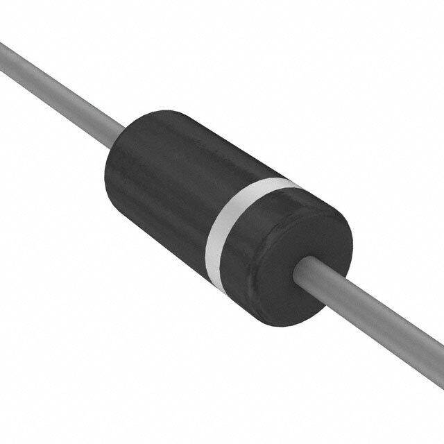
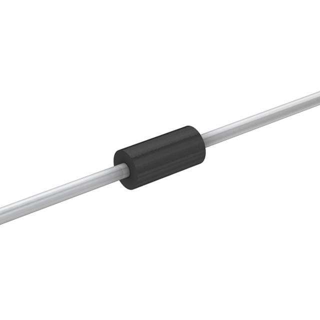
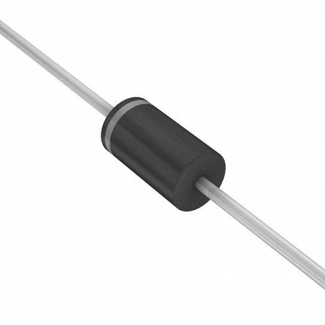
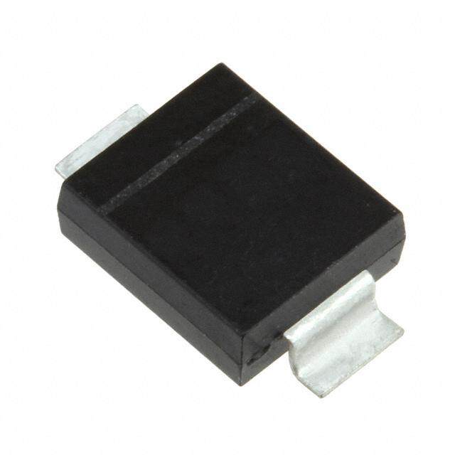
| 产品图片 |
|
| rohs | RoHS 合规性豁免 |
| 产品系列 | 二极管与整流器,TVS二极管,TVS 二极管 - 瞬态电压抑制器,Vishay Semiconductors P4SMA110A-E3/61 |
| 产品型号 | P4SMA110A-E3/61 |
| 产品种类 | TVS 二极管 - 瞬态电压抑制器 |
| 击穿电压 | 105 V |
| 商标 | Vishay Semiconductors |
| 商标名 | TransZorb |
| 安装风格 | SMD/SMT |
| 封装 | Reel |
| 封装/箱体 | DO-214AC |
| 尺寸 | 2.79(Max) mm W x 4.5 mm L |
| 峰值浪涌电流 | 40 A |
| 峰值脉冲功率耗散 | 400 W |
| 工作电压 | 94 V |
| 工厂包装数量 | 1800 |
| 最大工作温度 | + 150 C |
| 最小工作温度 | - 65 C |
| 极性 | Unidirectional |
| 端接类型 | SMD/SMT |
| 系列 | P4SMA |
| 钳位电压 | 152 V |


- 商务部:美国ITC正式对集成电路等产品启动337调查
- 曝三星4nm工艺存在良率问题 高通将骁龙8 Gen1或转产台积电
- 太阳诱电将投资9.5亿元在常州建新厂生产MLCC 预计2023年完工
- 英特尔发布欧洲新工厂建设计划 深化IDM 2.0 战略
- 台积电先进制程称霸业界 有大客户加持明年业绩稳了
- 达到5530亿美元!SIA预计今年全球半导体销售额将创下新高
- 英特尔拟将自动驾驶子公司Mobileye上市 估值或超500亿美元
- 三星加码芯片和SET,合并消费电子和移动部门,撤换高东真等 CEO
- 三星电子宣布重大人事变动 还合并消费电子和移动部门
- 海关总署:前11个月进口集成电路产品价值2.52万亿元 增长14.8%


PDF Datasheet 数据手册内容提取
P4SMA Series www.vishay.com Vishay General Semiconductor Surface-Mount TRANSZORB® Transient Voltage Suppressors FEATURES • Low profile package • Ideal for automated placement • Glass passivated chip junction • Available in uni-directional and bi-directional • 400 W peak pulse power capability with a Available 10/1000 μs waveform, repetitive rate (duty cycle): 0.01 % (300 W above 91 V) • Excellent clamping capability • Very fast response time SMA (DO-214AC) • Low incremental surge resistance • Meets MSL level 1, per J-STD-020, LF maximum peak of 260 °C • AEC-Q101 qualified available LINKS TO ADDITIONAL RESOURCES - Automotive ordering code: P/NHE3 or P/NHM3 • Material categorization: for definitions of complianc e 3DDD 333D please see www.vishay.com/doc?99912 3D Models TYPICAL APPLICATIONS Use in sensitive electronics protection against voltage PRIMARY CHARACTERISTICS transients induced by inductive load switching and lightin g V (uni-directional) 5.8 V to 459 V on ICs, MOSFET, signal lines of sensor units for consumer, WM computer, industrial, and telecommunication. V (bi-directional) 5.8 V to 185 V WM VBR (uni-directional) 6.8 V to 540 V MECHANICAL DATA V (bi-directional) 6.8 V to 220 V BR Case: SMA (DO-214AC) PPPM 400 W, 300 W Molding compound meets UL 94 V-0 flammability rating PD 3.3 W Base P/N-E3 - RoHS-compliant, commercial grade I (uni-directional only) 40 A Base P/N-M3 - halogen-free, RoHS-compliant, commercial FSM grade T max. 150 °C J Base P/NHE3_X - RoHS-compliant and AEC-Q101 qualified Polarity Uni-directional, bi-directional Base P/NHM3_X - halogen-free, RoHS-compliant, and Package SMA (DO-214AC) AEC-Q101 qualified (“_X” denotes revision code e.g. A, B, ...) DEVICES FOR BI-DIRECTION APPLICATIONS Terminals: matte tin plated leads, solderable per J-STD-002 and JESD 22-B102 For bi-directional devices use CA suffix (e.g. P4SMA10CA). E3, M3, HE3, and HM3 suffix meets JESD 201 class 2 Electrical characteristics apply in both directions. whisker test Polarity: for uni-directional types the band denotes cathod e end, no marking on bi-directional types MAXIMUM RATINGS (T = 25 °C unless otherwise noted) A PARAMETER SYMBOL VALUE UNIT Peak power dissipation with a 10/1000 μs waveform (1)(2) (fig. 1) P 400 W PPM Peak pulse current with a 10/1000 μs waveform (1) (fig. 3) I See next table A PPM Power dissipation on infinite heatsink at T = 50 °C P 3.3 W A D Peak forward surge current 8.3 ms single half sine-wave uni-directional only (2) I 40 A FSM Operating junction and storage temperature range T , T -65 to +150 °C J STG Notes (1) Non-repetitive current pulse, per fig. 3 and derated above T = 25 °C per fig. 2. Rating is 300 W above 91 V A (2) Mounted on 0.2" x 0.2" (5.0 mm x 5.0 mm) copper pads to each terminal Revision: 20-Jul-2020 1 Document Number: 88367 For technical questions within your region: DiodesAmericas@vishay.com, DiodesAsia@vishay.com, DiodesEurope@vishay.com THIS DOCUMENT IS SUBJECT TO CHANGE WITHOUT NOTICE. THE PRODUCTS DESCRIBED HEREIN AND THIS DOCUMENT ARE SUBJECT TO SPECIFIC DISCLAIMERS, SET FORTH AT www.vishay.com/doc?91000
P4SMA Series www.vishay.com Vishay General Semiconductor ELECTRICAL CHARACTERISTICS (T = 25 °C unless otherwise noted) A BREAKDOWN MAXIMUM MAXIMUM DEVICE MAXIMUM MAXIMUM VOLTAGE TEST STAND-OFF REVERSE PEAK PART MARKING V AT I (1) CURRENT VOLTAGE LEAKAGE PULSE CLAMPING TEMPERATURE CODE BR T VOLTAGE COEFFICIENT NUMBER (V) I V AT V CURRENT T WM WM AT I OF V (mA) (V) I (4) I (2) PPM BR UNI BI MIN. MAX. (DμA) PP(MA ) VC (V) (%/°C) (+)P4SMA6.8A 6V8A 6V8C 6.45 7.14 10 5.80 1000 38.1 10.5 0.057 (+)P4SMA7.5A 7V5A 7V5C 7.13 7.88 10 6.40 500 35.4 11.3 0.061 (+)P4SMA8.2A 8V2A 8V2C 7.79 8.61 10 7.02 200 33.1 12.1 0.065 (+)P4SMA9.1A 9V1A 9V1C 8.65 9.55 1.0 7.78 50 29.9 13.4 0.068 (+)P4SMA10A 10A 10C 9.5 10.5 1.0 8.55 10 27.6 14.5 0.073 (+)P4SMA11A 11A 11C 10.5 11.6 1.0 9.40 5.0 25.6 15.6 0.075 (+)P4SMA12A 12A 12C 11.4 12.6 1.0 10.2 1.0 24.0 16.7 0.078 (+)P4SMA13A 13A 13C 12.4 13.7 1.0 11.1 1.0 22.0 18.2 0.081 (+)P4SMA15A 15A 15C 14.3 15.8 1.0 12.8 1.0 18.9 21.2 0.084 (+)P4SMA16A 16A 16C 15.2 16.8 1.0 13.6 1.0 17.8 22.5 0.086 (+)P4SMA18A 18A 18C 17.1 18.9 1.0 15.3 1.0 15.9 25.2 0.089 (+)P4SMA20A 20A 20C 19.0 21.0 1.0 17.1 1.0 14.4 27.7 0.090 (+)P4SMA22A 22A 22C 20.9 23.1 1.0 18.8 1.0 13.1 30.6 0.092 (+)P4SMA24A 24A 24C 22.8 25.2 1.0 20.5 1.0 12.0 33.2 0.090 (+)P4SMA27A 27A 27C 25.7 28.4 1.0 23.1 1.0 10.7 37.5 0.096 (+)P4SMA30A 30A 30C 28.5 31.5 1.0 25.6 1.0 9.7 41.4 0.097 (+)P4SMA33A 33A 33C 31.4 34.7 1.0 28.2 1.0 8.8 45.7 0.098 (+)P4SMA36A 36A 36C 34.2 37.8 1.0 30.8 1.0 8.0 49.9 0.099 (+)P4SMA39A 39A 39C 37.1 41.0 1.0 33.3 1.0 7.4 53.9 0.100 (+)P4SMA43A 43A 43C 40.9 45.2 1.0 36.8 1.0 6.7 59.3 0.101 (+)P4SMA47A 47A 47C 44.7 49.4 1.0 40.2 1.0 6.2 64.8 0.101 (+)P4SMA51A 51A 51C 48.5 53.6 1.0 43.6 1.0 5.7 70.1 0.102 (+)P4SMA56A 56A 56C 53.2 58.8 1.0 47.8 1.0 5.2 77.0 0.103 (+)P4SMA62A 62A 62C 58.9 65.1 1.0 53.0 1.0 4.7 85.0 0.104 (+)P4SMA68A 68A 68C 64.6 71.4 1.0 58.1 1.0 4.3 92.0 0.104 (+)P4SMA75A 75A 75C 71.3 78.8 1.0 64.1 1.0 3.9 104 0.105 (+)P4SMA82A 82A 82C 77.9 86.1 1.0 70.1 1.0 3.5 113 0.105 (+)P4SMA91A 91A 91C 86.5 95.5 1.0 77.8 1.0 3.2 125 0.106 (+)P4SMA100A 100A 100C 95.0 105 1.0 85.5 1.0 2.2 137 0.106 (+)P4SMA110A 110A 110C 105 116 1.0 94.0 1.0 2.0 152 0.107 (+)P4SMA120A 120A 120C 114 126 1.0 102 1.0 1.8 165 0.107 (+)P4SMA130A 130A 130C 124 137 1.0 111 1.0 1.7 179 0.107 (+)P4SMA150A 150A 150C 143 158 1.0 128 1.0 1.4 207 0.106 (+)P4SMA160A 160A 160C 152 168 1.0 136 1.0 1.4 219 0.108 (+)P4SMA170A 170A 170C 162 179 1.0 145 1.0 1.3 234 0.108 (+)P4SMA180A 180A 180C 171 189 1.0 154 1.0 1.2 246 0.108 (+)P4SMA200A 200A 200C 190 210 1.0 171 1.0 1.1 274 0.108 (+)P4SMA220A 220A 220C 209 231 1.0 185 1.0 0.91 328 0.108 P4SMA250A 250A - 237 263 1.0 214 1.0 0.87 344 0.110 P4SMA300A 300A - 285 315 1.0 256 1.0 0.73 414 0.110 P4SMA350A 350A - 333 368 1.0 300 1.0 0.62 482 0.110 P4SMA400A 400A - 380 420 1.0 342 1.0 0.55 548 0.110 P4SMA440A 440A - 418 462 1.0 376 1.0 0.50 602 0.110 P4SMA480A 480A - 456 504 1.0 408 1.0 0.46 658 0.110 P4SMA510A 510A - 485 535 1.0 434 1.0 0.43 698 0.110 P4SMA540A 540A - 513 567 1.0 459 1.0 0.41 740 0.110 Notes (1) Pulse test: t ≤ 50 ms p (2) Surge current waveform per fig. 3 and derate per fig. 2 (3) All terms and symbols are consistent with ANSI/IEEE CA62.35 (4) For bi-directional types with V of 10 V and less, the I limit is doubled R D (5) V = 3.5 V at I = 25 A (uni-directional only) F F (+) Underwriters Laboratory Recognition for the classification of protectors (QVGQ2) under the UL standard for safety 497B and file number E136766 for both uni-directional and bi-directional device Revision: 20-Jul-2020 2 Document Number: 88367 For technical questions within your region: DiodesAmericas@vishay.com, DiodesAsia@vishay.com, DiodesEurope@vishay.com THIS DOCUMENT IS SUBJECT TO CHANGE WITHOUT NOTICE. THE PRODUCTS DESCRIBED HEREIN AND THIS DOCUMENT ARE SUBJECT TO SPECIFIC DISCLAIMERS, SET FORTH AT www.vishay.com/doc?91000
P4SMA Series www.vishay.com Vishay General Semiconductor THERMAL CHARACTERISTICS (T = 25 °C unless otherwise noted) A PARAMETER SYMBOL VALUE UNIT Typical thermal resistance, junction to ambient air (1) RθJA 120 °C/ W Typical thermal resistance, junction to lead RθJL 30 Note (1) Mounted on minimum recommended pad layout ORDERING INFORMATION (Example) VOLTAGE RANGE PREFERRED P/N UNIT WEIGHT (V) PACKAGE BASE DELIVERY MODE (g) CODE QUANTITY UNI - BI - P4SMA6.8A-E3/61 0.064 6.8 to 220 6.8 to 220 61 1800 7" diameter plastic tape and reel P4SMA6.8A-M3/61 0.064 6.8 to 540 6.8 to 220 61 1800 7" diameter plastic tape and reel P4SMA6.8A-E3/5A 0.064 6.8 to 220 6.8 to 220 5A 7500 13" diameter plastic tape and reel P4SMA6.8A-M3/5A 0.064 6.8 to 540 6.8 to 220 5A 7500 13" diameter plastic tape and reel P4SMA6.8AHE3_A/H (1) 0.064 6.8 to 220 6.8 to 220 H 1800 7" diameter plastic tape and reel P4SMA6.8AHM3_A/H (1) P4SMA6.8AHE3_A/I (1) 0.064 6.8 to 220 6.8 to 220 I 7500 13" diameter plastic tape and reel P4SMA6.8AHM3_A/I (1) P4SMA250AHM3_B/H (2) 0.064 250 to 540 - H 1800 7" diameter plastic tape and reel P4SMA250AHM3_B/I (2) 0.064 250 to 540 - I 7500 13" diameter plastic tape and reel Notes (1) _A is available for P4SMA6.8(C)A to P4SMA220(C)A, AEC-Q101 qualified (2) _B is available for P4SMA250A to P4SMA540A, AEC-Q101 qualified RATINGS AND CHARACTERISTICS CURVES (T = 25 °C unless otherwise noted) A 100 100 Non-Repetitive Pulse )PP )Wk( rewoP esluP kaeP - MP 101 PP44SSMMAA150400AA - WTAa =ve PP2fo544r SS°mMMC sAAh69o.1w8AAn -in Fig. 3 I( tnerruC ro )P( rewoP esluPP% ,egatnecreP ni gnitareD 752505 PP 0.2 x 0.2" (5.0 x 5.0 mm) P k Copper Pad Areas ae 0.1 P 0 0.1 µs 1.0 µs 10 µs 100 µs 1.0 ms 10 ms 0 25 50 75 100 125 150 175 200 td - Pulse Width (s) TJ - Initial Temperature (°C) Fig. 1 - Peak Pulse Power Rating Curve Fig. 2 - Pulse Power or Current vs. Initial Junction Temperature Revision: 20-Jul-2020 3 Document Number: 88367 For technical questions within your region: DiodesAmericas@vishay.com, DiodesAsia@vishay.com, DiodesEurope@vishay.com THIS DOCUMENT IS SUBJECT TO CHANGE WITHOUT NOTICE. THE PRODUCTS DESCRIBED HEREIN AND THIS DOCUMENT ARE SUBJECT TO SPECIFIC DISCLAIMERS, SET FORTH AT www.vishay.com/doc?91000
P4SMA Series www.vishay.com Vishay General Semiconductor 150 1000 MSR tr = 10 µs iTPsJu dl=se e2fi n5We °idCd tahs ( tthd)e Point )W/C I % ,tne 100 PIPePaMk Value wdehcearyes t htoe 5P0e a%k oCfu IrPrPeMnt °( ecna 100 rru de C p esluP kaeP - IMPP 50 td HIPaPMlf Val1au0se / d1-e0f0IiP2n0P e µds b Wy aRv.eEf.oAr.m mI lamrehT tneisnarT 10 0 1 0 1.0 2.0 3.0 4.0 0.001 0.01 0.1 1 10 100 1000 t - Time (ms) t - Pulse Duration (s) p Fig. 3 - Pulse Waveform Fig. 5 - Typical Transient Thermal Impedance 10 000 200 TJ = 25 °C TJ = TJ max. e (pF) fVM =sei g1a =.s0 u5 rM0e Hdm zaVtp-p ent (A) 100 8.3 ms Single Half Sine-Wave apacitanc1000 SVotaUltnandgi--eDO iVfrfeWcMtional urge Curr 50 C S n d ctio 100 war C - JunJ Bi-Directional Peak For 10 10 1 10 100 200 1 5 10 50 100 V - Breakdown Voltage (V) Number of Cycles at 60 Hz BR Fig. 4 - Typical Junction Capacitance Fig. 6 - Maximum Non-Repetitive Forward Surge Current Uni-Directional Use Only Revision: 20-Jul-2020 4 Document Number: 88367 For technical questions within your region: DiodesAmericas@vishay.com, DiodesAsia@vishay.com, DiodesEurope@vishay.com THIS DOCUMENT IS SUBJECT TO CHANGE WITHOUT NOTICE. THE PRODUCTS DESCRIBED HEREIN AND THIS DOCUMENT ARE SUBJECT TO SPECIFIC DISCLAIMERS, SET FORTH AT www.vishay.com/doc?91000
P4SMA Series www.vishay.com Vishay General Semiconductor PACKAGE OUTLINE DIMENSIONS in inches (millimeters) SMA (DO-214AC) Cathode Band Mounting Pad Layout 0.066 (1.68) 0.074 (1.88) MIN. MAX. 0.065 (1.65) 0.110 (2.79) 0.049 (1.25) 0.100 (2.54) 0.177 (4.50) 0.157 (3.99) 0.060 (1.52) 0.012 (0.305) MIN. 0.006 (0.152) 0.208 (5.28) 0.090 (2.29) REF. 0.078 (1.98) 0.060 (1.52) 0.030 (0.76) 0.008 (0.203) 0 (0) 0.208 (5.28) 0.194 (4.93) Revision: 20-Jul-2020 5 Document Number: 88367 For technical questions within your region: DiodesAmericas@vishay.com, DiodesAsia@vishay.com, DiodesEurope@vishay.com THIS DOCUMENT IS SUBJECT TO CHANGE WITHOUT NOTICE. THE PRODUCTS DESCRIBED HEREIN AND THIS DOCUMENT ARE SUBJECT TO SPECIFIC DISCLAIMERS, SET FORTH AT www.vishay.com/doc?91000
Legal Disclaimer Notice www.vishay.com Vishay Disclaimer ALL PRODUCT, PRODUCT SPECIFICATIONS AND DATA ARE SUBJECT TO CHANGE WITHOUT NOTICE TO IMPROV E RELIABILITY, FUNCTION OR DESIGN OR OTHERWISE. Vishay Intertechnology, Inc., its affiliates, agents, and employees, and all persons acting on its or their behalf (collectively, “Vishay”), disclaim any and all liability for any errors, inaccuracies or incompleteness contained in any datasheet or in any other disclosure relating to any product. Vishay makes no warranty, representation or guarantee regarding the suitability of the products for any particular purpose o r the continuing production of any product. To the maximum extent permitted by applicable law, Vishay disclaims (i) any and all liability arising out of the application or use of any product, (ii) any and all liability, including without limitation special, consequential or incidental damages, and (iii) any and all implied warranties, including warranties of fitness for particular purpose, non-infringement and merchantability. Statements regarding the suitability of products for certain types of applications are based on Vishay’s knowledge of typical requirements that are often placed on Vishay products in generic applications. Such statements are not binding statements about the suitability of products for a particular application. It is the customer’s responsibility to validate that a particular product with the properties described in the product specification is suitable for use in a particular application. Parameters provided in datasheets and / or specifications may vary in different applications and performance may vary over time. All operating parameters, including typical parameters, must be validated for each customer application by the customer’s technical experts. Product specifications do not expand or otherwise modify Vishay’s terms and conditions of purchase, including but not limited to the warranty expressed therein. Except as expressly indicated in writing, Vishay products are not designed for use in medical, life-saving, or life-sustainin g applications or for any other application in which the failure of the Vishay product could result in personal injury or death. Customers using or selling Vishay products not expressly indicated for use in such applications do so at their own risk . Please contact authorized Vishay personnel to obtain written terms and conditions regarding products designed for such applications. No license, express or implied, by estoppel or otherwise, to any intellectual property rights is granted by this documen t or by any conduct of Vishay. Product names and markings noted herein may be trademarks of their respective owners. © 2019 VISHAY INTERTECHNOLOGY, INC. ALL RIGHTS RESERVED Revision: 01-Jan-2019 1 Document Number: 91000